EP0426120A2 - Circuit amplificateur à linéarité améliorée - Google Patents
Circuit amplificateur à linéarité améliorée Download PDFInfo
- Publication number
- EP0426120A2 EP0426120A2 EP90120817A EP90120817A EP0426120A2 EP 0426120 A2 EP0426120 A2 EP 0426120A2 EP 90120817 A EP90120817 A EP 90120817A EP 90120817 A EP90120817 A EP 90120817A EP 0426120 A2 EP0426120 A2 EP 0426120A2
- Authority
- EP
- European Patent Office
- Prior art keywords
- transistor
- signal
- input
- differential amplifier
- current
- Prior art date
- Legal status (The legal status is an assumption and is not a legal conclusion. Google has not performed a legal analysis and makes no representation as to the accuracy of the status listed.)
- Granted
Links
Images


Classifications
-
- H—ELECTRICITY
- H03—ELECTRONIC CIRCUITRY
- H03F—AMPLIFIERS
- H03F3/00—Amplifiers with only discharge tubes or only semiconductor devices as amplifying elements
- H03F3/68—Combinations of amplifiers, e.g. multi-channel amplifiers for stereophonics
-
- H—ELECTRICITY
- H03—ELECTRONIC CIRCUITRY
- H03F—AMPLIFIERS
- H03F1/00—Details of amplifiers with only discharge tubes, only semiconductor devices or only unspecified devices as amplifying elements
- H03F1/32—Modifications of amplifiers to reduce non-linear distortion
- H03F1/3211—Modifications of amplifiers to reduce non-linear distortion in differential amplifiers
Definitions
- This invention generally relates to an amplification circuit, and particularly relates to an amplification circuit with improved linearity. This invention has particular applicability to an amplification circuit making use of a differential amplifier.
- amplification circuit linearity is required between an input signal and an output signal in a wide range of input signal level.
- a receiving circuit for use in a codeless telephone, in a transceiver and the like is provided with an amplification circuit for amplifying received voice signals.
- some noise other than a voice signal is included in a received radiowave. This means that when the level of the voice signal is low, the noise comes to be relatively more prominent compared to the voice signal. It is therefore necessary to amplify the voice signal by the amplification circuit. In particular, as the voice signal changes over a wide range of signal level, the amplification circuit is required to have a wide dynamic range, i.e. linearity between the input and output.
- a differential amplifier is frequently used in an amplification circuit for various electrical signals, and it is used in the amplification circuit for the above mentioned voice signal.
- the differential amplifier itself has non-linearity between the input signal and the output signal, it is often the case that the amplified voice signal has distortion. To begin with, description will be given on this point.
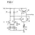
- Fig. 1 is a circuit diagram of a conventional amplification circuit.
- this amplification circuit comprises a first differential amplifier composed of npn transistors 1 and 2, constant current sources 3 and 4, and resistor 5; a second differential amplifier composed of diodes 6 and 7 for converting an output signal generated from the differential amplifier into a logarithmic signal, npn transistors 8 and 9 and a variable current source 10, and a current mirror circuit composed of pnp transistors 11 and 12.
- the second differential amplifier and the current mirror circuit form an exponential conversion circuit for exponent- converting a logarithm converted signal.
- the transistor 1 has its base connected to receive an input signal V.
- the transistor 2 has its base connected to receive a predetermined constant voltage V B .
- the transistor 1 is grounded through a constant voltage source 3 with an emitter capable of passing a constant current I D .
- the transistor 2 is grounded through a constant current source 4 with an emitter capable of passing a constant current I D .
- the resistor 5 is connected between the emitters of the transistors 1 and 2. The resistor 5 is provided to increase the gain of the first differential amplifier.
- Each diodes 6 and 7 are connected between a power supply Vcc and the collectors of the transistors 1 and 2 respectively.
- the transistor 8 has its base connected to the collector of the transistor 2.
- the transistor 9 has its base connected to the collector of the transistor 1.
- the transistors 8 and 9 have the emitters connected together, and between the common connection node and ground, the variable current source 10 capable of passing a variable current I G is connected.
- the transistor 11 connected to a diode is connected between the power supply Vcc and the collector of the transistor 8.
- the transistor 12 is connected between the power supply Vcc and the transistor 9. An output current Io is generated through the common connection node of the transistors 9 and 12.
- the input signal V is applied to the base of the transistor 1, and then the applied input signal V is converted into a current signal by the transistors 1 and 2.
- the converted current signal is converted into a logarithmic signal by the diodes 6 and 7.
- the two logarithm-converted signals are applied to the bases of the transistors 8 and 9.
- the output current I O determined based on the product of the voltage between the bases of the transistors 8 and 9 and the variable current I G is thus output through the collector of the transistor 9.
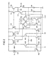
- Fig. 2 is a circuit diagram of a conventional multiplying circuit making use of the differential amplifier indicated in Fig. 1.
- this multiplying circuit comprises a first differential amplifier composed of npn transistors 103, 104, 106 and 107, and a resistor 108; a current mirror circuit composed of pnp transistors 109 and 110; a current mirror circuit composed of pnp transistors 111 and 112; a multiplier composed of pnp transistors 121, 122, 123 and 124; and a second differential amplifier composed of pnp transistors 116 and 117 and a resistor 118.
- This multiplication circuit receives the input signals V L and V R to generate an output current I OUT determined by multiplication of V L and V R .
- the input signal V L is applied to the base of the transistor 106, the input signal V L is converted into a current signal by the transistors 106, 107, and a resistor 108.
- the collector current of the transistor 106 is applied to the emitters of the transistors 121 and 122 through the transistors 109 and 110.
- the collector current of the transistor 107 is applied to the emitters of the transistors 123 and 124 through the transistors 111 and 112.
- the input signal V R is applied to the base of the transistor 116, the input signal V R is converted into a current signal by the transistors 116, 117, and the resistor 118.
- the respective collector current of the transistors 116 and 117 are converted into logarithmic signals by the diodes 119 and 120 respectively.
- the two converted signals are applied to the bases of 122 and 123, and the bases of the transistors 121 and 124 respectively.
- multiplication of V L and V R is carried out by the transistors 121, 122, 123 and 124 whereby the current I OUT is obtained.
- the multiplication circuit indicated in Fig. 2 also creates the similar problem observed in the amplification circuit indicated in Fig. 1. Description will be given on this point in the following.
- the resistor 108 is connected between the emitters of the transistors 106 and 107 which form the first differential amplifier.
- the non-linear emitter resistance of the transistors 106 and 107 included therein therefore cannot be ignored, when the input signal V L is converted into a current signal.
- the resistance 118 is connected between the emitters of the transistors 116 and 117, in current conversion of the input signal V R , the non-linear emitter resistance of the transistors 116 and 117 cannot be ignored.
- I E1 , I E2 and I OUT will be represented by the following equations.
- I E1 (V L - V B /(R1 + 2 ⁇ r e ) (2)
- I E2 (V R - V B )/(R2 + 2 ⁇ r e ) (3)
- I OUT 2 ⁇ I E1 ⁇ I E2 /I D (4)
- I OUT 2 ⁇ (V L - V B )/(R1 + 2 ⁇ r e ) ⁇ ⁇ (V R - V B / (R2 + 2 ⁇ r e ( ⁇ ⁇ (1/I D ) (5)
- the value 2 ⁇ r e is preferable for the value 2 ⁇ r e to be negligible, in order to secure the good non-linearity of the multiplication circuit indicated in Fig. 2.
- each internal resistance of the emitter r of the transistors 106, 107, 116 and 117 is necessary therefore for each internal resistance of the emitter r of the transistors 106, 107, 116 and 117 to be reduced by making the relation of the values represented by R1 » 2 ⁇ r e and R2 » 2 ⁇ r e or by increasing the emitter currents I E1 and I E2 .
- R1 » 2 ⁇ r e and R2 » 2 ⁇ r e or by increasing the emitter currents I E1 and I E2 .
- One object of the present invention is to improve the linearity in an amplification circuit including a deferential amplifier for securing the wide dynamic range.
- An additional object of the present invention is to improve the linearity of an amplification circuit including a differential amplifier, without causing decrease in the gain.
- Another object of the present invention is to improve the linearity of an amplification circuit including a differential amplifier, without causing increase in current consumption.
- Yet another object of the present invention is to improve the linearity of a multiplication circuit including a differential amplifier without causing decrease in the gain.
- a further object of the present invention is to improve the linearity of a multiplication circuit including a differential amplifier, without causing increase in current consumption.
- the amplification circuit in accordance with the present invention comprises a current conversion circuit for converting an applied input signal into a current signal, and a first differential amplifier including first and second bipolar transistors.
- the first and second bipolar transistors have their emitters connected together.
- the first bipolar transistor has its base connected to receive the current signal converted by the current conversion circuit.
- This amplification circuit further comprises a comparison circuit for comparing the base potential of the first bipolar transistor and a predetermined potential, and a voltage control circuit for controlling the voltage between the base and emitter of the first bipolar transistor.
- the second bipolar transistor has its base connected to receive an output signal generated from the comparison circuit.
- the voltage control circuit responds to the comparison circuit and then controls the voltage between the base and emitter of the first bipolar transistor forming the first differential amplifier thereby keeping the emitter resistance of the first bipolar transistor constant.
- the first bipolar transistor is responsive only to the current signal converted by the current conversion circuit to operate, the linearity between the input signal and the output signal can be improved.
- the multiplication circuit comprises the current conversion circuit for converting a first input signal into a current signal, and the first differential amplifier including the first and second bipolar transistors.
- the first and second bipolar transistors have the emitters connected together.
- the first bipolar transistor has its base connected to receive the current signal converted by the current conversion circuit.
- This multiplication circuit further comprises a comparison circuit for comparing the base potential of the first bipolar transistor and a predetermined potential, a voltage control circuit controlling the voltage between the base and emitter of the first bipolar transistor, and a second differential amplifier including third and fourth bipolar transistors.
- the second bipolar transistor has its base connected to receive an output signal generated from the comparison circuit.
- the third bipolar transistor has its base connected to receive a second input signal.
- the fourth bipolar transistor has its base connected to the predetermined potential.
- This multiplication circuit further comprises a multiplication circuit for multiplying output signals generated from the first and second differential amplifiers.
- the amplification circuit indicating one embodiment of the present invention, comprises a first differential amplifier composed of npn transistors 20, 21 and 22, a second differential amplifier composed of npn transistors 18, 19 and 22, a logarithm conversion circuit composed of diodes 31 and 32, a third differential amplifier composed of npn transistors 33, 34, and a variable current source 35 passing a variable current I G , a fourth differential amplifier composed of npn transistors 24, 25 and 28.
- a current mirror circuit is composed of npn transistors 13, 14, 22, 28 and 30.
- a constant current source 15 which passes a predetermined constant current I D and a diode connected npn transistor 13 are connected in series between the power supply V CC and ground. The emitters of the transistors 13 and 14 are grounded. Pnp transistors 16 and 17 composing a current mirror circuit are connected together to the power supply V CC . The diode connected transistor 16 has its collector connected to the collector of the transistor 14. The current I D therefore flows through the collector of the transistor 17.
- the transistor 18 has its collector connected to the collector of the transistor 17.
- the transistor 19 has its collector connected to the power supply V CC . Since the transistor 18 has its collector and base connected together, the collector output is all fed back to the base.
- the bases of the transistors 18 and 20 are connected together and the common connection node thereof is connected to receive an input signal V through a resistor 23.
- the transistors 18, 19, 20 and 21 have the emitters connected together, and the transistor 22 is connected between the common connection node and ground.
- the transistor 22 has 4 times as large transistor size as that of the transistor 14, and acts as a constant current source.
- the transistor 22 has its base connected to the base of the transistor 14.
- the transistor 24 has its base connected to the base of the transistor 18.
- the transistor 25 has its base connected to receive a predetermined constant voltage V B .
- the transistors 24 and 25 have the emitters connected together, and a transistor 28 is connected between the common connection node and ground.
- the transistor 28 has its base connected to the base of the transistor 14.
- the transistor 28 therefore acts as a constant current source.
- a current mirror circuit is composed of pnp transistors 26 and 27.
- the diode-connected transistor 26 is connected between the power supply V CC and the collector of the transistor 24.
- the transistor 27 is connected between the power supply V CC and the collector of the transistor 25.
- a pnp transistor 29 is connected between the power supply V CC and the collector of the transistor 30 thereby forming a negative feed back circuit. That is, the transistor 29 has its base connected to the collector of the transistor 25, its emitter connected to the power supply, and its collector connected to the base of the transistor 19.
- a diode 31 is connected between the power supply and the collector of the transistor 20.
- a diode 32 is connected between the power supply Vcc and the collector of the transistor 21.
- Each base of the transistors 33 and 34 are connected to the cathodes of the diodes 32 and 31 respectively.
- a current mirror circuit is composed of pnp transistors 36 and 37.
- the diode-connected transistor 36 is connected between the power supply Vcc and the collector of the transistor 33.
- the transistor 37 is connected between the power supply Vcc and the collector of the transistor 34.
- An input signal V is converted into a current signal by the resistor 23.
- the first differential amplifier composed of the transistors 20, 21 and 22 responds to the converted current signal and operate.
- Output signal from the first differential amplifier is converted into logarithm signals by the diodes 31 and 32, and the converted signals are supplied to the bases of the transistors 33 and 34 respectively.
- the third differential amplifier composed of the transistors 33, 34, and the variable current source 35 converts the logarithmic signal into an exponential function.
- the output current I O which does not include logarithmic and exponential functions is thus generated.
- the base of the transistor 20 is provided with negative feed back, and the base potential of the transistor 20 is kept at a virtual ground potential. Description will be given on this point in the following.
- the base current of the transistor 20 i.e. the base current of the transistor 18 increases, the base current of the transistor 24 increases accordingly. Since much more collector current flows through the transistors 26 and 27 in response to the increase in the base current of the transistor 24, the base current of the transistor 29 is increased. The base current of the transistor 19 is decreased and the base current of the transistor 18 is decreased accordingly. On the other hand, when the base current of the transistor 18 decreases, the base current of the transistor 24 decreases accordingly.
- the base current of the transistor 29 is decreased.
- the base current of the transistor 19 is thus increased, and the base current of the transistor 18 is increased accordingly.
- the first differential amplifier composed of the transistors 18, 19 and 22 are always provided with negative feed back.
- the base current of the transistor 20 is thus kept at a constant potential, i.e. at a virtual ground potential.
- voltage V BE between the base and emitters of the transistors 18 and 20 are kept at a constant value.
- the internal resistance of the emitter r e of the transistors 18 and 20 are kept constant accordingly.
- the input signal V is to be converted into a current signal only by the resistor 23, without taking into consideration of the non-linear internal resistance of the emitter r e of the transistors 18 and 20.
- the emitter current I E changes in proportion with the input signal V.
- improvement can be achieved on the linearity between the input and output of the first differential amplifier composed of the transistors 20, 21 and 22, whereby the overall linearity of the amplification circuit indicated in Fig. 3 can be improved compared to the conventional circuit indicated in Fig. 1.
- the amplification circuit indicated in Fig. 3 comprises the logarithm conversion circuit composed of the diodes 31 and 32, and the exponent conversion circuit composed of the transistors 33, 34, 36 and 37m and the, variable current source 35.
- Each of the diode 31 and 32 converts the collector currents of the transistor 20 and 21 into logarithmic signals respectively.
- I E2 I S ⁇ exp ( ⁇ V BE /2 ⁇ V T ) (7)
- the output current Io determined in accordance with the product (linear multiplication) of the input signal V and the ourrent value I G can be obtained, by changing the current value I G generated from the variable current source 35.
- this multiplication circuit comprises a first differential amplifier composed of npn transistors 137, 138 and 129; a second differential amplifier composed of npn transistors 135, 136 and 129; a third differential amplifier composed of npn transistors 141, 142 and 131; a multiplier composed of pnp transistors 121, 122, 123 and 124; and a fourth differential amplifier composed of pnp transistors 114, 115, 116 and 117 and a resistor 118.
- a current mirror circuit is formed of npn transistors 127, 128, 129, 130, 131 and 132.
- a current mirror circuit is composed of pnp transistors 113, 114 and 115.
- the diode-connected transistor 127 has its collector connected to receive a constant current I D through a constant current source 101.
- the emitters of the transistors 127 to 131 are grounded.
- the transistor 129 has 4 times as large value as the transistors 127, 128, 130, 131 and 132 in transistor size.
- a current mirror circuit is composed of pnp transistors 133 and 134.
- the diode connected transistor 133 has its collector connected to the collector of the transistor 128.
- the emitters of the transistors 133 and 134 are connected to the power supply Vcc.
- the transistor 135 has its collector connected to the collector of the transistor 134.
- the transistor 136 has its collector connected to the power supply Vcc. As the transistor 135 has its collector and base connected together, the collector output is all fed back to the base.
- the base of the transistor 135 is connected to receive a first input signal V L through a resistor 139 for current conversion.
- the base of the transistor 137 is connected to the base of the transistor 135.
- the base of the transistor 138 is connected to that of the transistor 136.
- the transistors 135, 136, 137 and 138 have their emitters connected together, and between the common connection node and ground the transistor 129 is connected.
- the base of the transistor 141 is connected to the collector of the transistor 135.
- the transistor 142 has its base connected to a predetermined constant voltage V B .
- the transistors 141 and 142 have their emitters connected together, and between the common connection node and ground the transistor 131 is connected.
- Pnp transistors 143 and 144 form a current mirror circuit.
- the transistors 143 and 144 have each emitter connected to the power supply Vcc.
- Each collector of the transistors 143 and 144 are connected to the collectors of the transistors 141 and 142 respectively.
- the pnp transistor 145 for negative feed back has its base connected to the collector of the transistor 144, its emitter connected to the power supply Vcc, and its collector connected together to the base of the transistor 136 and the collector of the transistor 130.
- the transistors 135 and 137 always have their bases provided with negative feedback. Furthermore, as the transistor 135 undergoes not only a negative feedback but also a total feedback, the base of the transistor 135 is brought to a constant potential, i.e. a virtual ground potential. As a result, the supply of AC signal component to the base of the transistor 135 can be prevented.
- the base emitter voltage V BE of the transistor 137 is therefore kept at a constant value by negative feed back operation.
- the internal resistance of the emitter r e of the transistor 137 does not change in accordance with the change of the emitter current I E . Since the transistor 137 responds only to the current signal converted by the resistor 139 and operates, good linearity can be secured between the input and the output of the first differential amplifier composed of the transistors 137, 138 and 129.
- Pnp transistors 146 and 147 form a current mirror circuit.
- the emitters of the transistors 146 and 147 are connected to the power supply Vcc.
- the diode connected transistor 146 has its collector connected to the collector of the transistor 137.
- the transistor 147 has its collector connected to the emitters of the transistor 121 and 122.
- the collector current of the transistor 137 is therefore applied to the emitters of the transistors 121 and 122 through the transistors 146 and 147.
- Pnp transistors 148 and 149 form a current mirror circuit.
- the transistors 148 and 149 have their emitters connected to the power supply Vcc.
- the diode connected transistor 148 has its collector connected to the collector of the transistor 138.
- the collector of the transistor 149 is connected to the emitters of the transistors 122 and 124.
- the collector current of the transistor 138 is therefore applied to the emitters of the transistors 123 and 124 through the transistors 148 and 149.
- I E3 I S ⁇ exp (V BE /V T ) (9) where, I S is a backward saturation current, V BE is the voltage between base and emitter, and V T is a constant.
- ⁇ V BE ′ 2 ⁇ V T ⁇ log (I E4 /I S ) (10) where I E4 is the output current.
- a fifth differential amplifier composed of the transistors 121, 122, 123 and 124 is supplied with the collector output of the transistors 147 and 149, and the collector output of the transistors 116 and 117.
- the emitter current I E3 will be removed of both logarithmic function and exponential function.
- the fifth differential amplifier therefore generates an output current I OUT which does not follow the logarithmic function and exponential function.
- the output current I OUT can be obtained, which is determined by the multiplication (linear multiplication) of the first input signal V L and the second input signal V R .
- the linearity between the input and the output of the differential amplifier is improved in the above mentioned manner, in order to expend the dynamic range of the first input signal V L .
- a circuit surrounded by a chain dotted line in Fig. 4 is provided in place of the transistors 116, 117 and the resistor 118.
- the base of the transistor constituting the first differential amplifier is kept at a constant potential, i.e. a virtual ground potential, the value of the internal resistance of the emitter r e does not change in accordance with the change of the emitter current.
- the transistor responds only to the current signal based on the input signal, the linearity between the input and the output of the first differential amplifier is improved.
- the wide dynamic ranges of the amplification circuit and multiplication circuit indicated in Figs. 3 and 4 are secured, thereby improving the linearity. Since the current needs not to be increased in reducing the effect of internal resistance of the emitter, current consumption is not increased.
Landscapes
- Engineering & Computer Science (AREA)
- Power Engineering (AREA)
- Physics & Mathematics (AREA)
- Nonlinear Science (AREA)
- Amplifiers (AREA)
Applications Claiming Priority (4)
| Application Number | Priority Date | Filing Date | Title |
|---|---|---|---|
| JP1283904A JPH0744396B2 (ja) | 1989-10-31 | 1989-10-31 | 増幅器 |
| JP283904/89 | 1989-10-31 | ||
| JP288248/89 | 1989-11-06 | ||
| JP1288248A JP2783875B2 (ja) | 1989-11-06 | 1989-11-06 | 増幅器 |
Publications (3)
| Publication Number | Publication Date |
|---|---|
| EP0426120A2 true EP0426120A2 (fr) | 1991-05-08 |
| EP0426120A3 EP0426120A3 (en) | 1991-08-21 |
| EP0426120B1 EP0426120B1 (fr) | 1996-01-17 |
Family
ID=26555246
Family Applications (1)
| Application Number | Title | Priority Date | Filing Date |
|---|---|---|---|
| EP90120817A Expired - Lifetime EP0426120B1 (fr) | 1989-10-31 | 1990-10-30 | Circuit amplificateur à linéarité améliorée |
Country Status (4)
| Country | Link |
|---|---|
| US (1) | US5065112A (fr) |
| EP (1) | EP0426120B1 (fr) |
| KR (1) | KR970003778B1 (fr) |
| DE (1) | DE69024914T2 (fr) |
Cited By (2)
| Publication number | Priority date | Publication date | Assignee | Title |
|---|---|---|---|---|
| EP0669710A3 (fr) * | 1994-02-24 | 1997-06-11 | Toshiba Kk | Circuit d'amplification à gain variable. |
| GB2329774A (en) * | 1997-09-26 | 1999-03-31 | Nec Corp | A transconductance amplifier with a V-I converter and a diode load for producing a logarithmic output which is then exponentiated to give a linear output |
Families Citing this family (4)
| Publication number | Priority date | Publication date | Assignee | Title |
|---|---|---|---|---|
| EP0490016B1 (fr) * | 1990-12-12 | 1995-08-09 | STMicroelectronics S.r.l. | Circuit intégré pour engendrer un courant indépendant de la température, proportionnel à la différence de tension entre un signal et une tension de référence |
| US5432477A (en) * | 1992-07-31 | 1995-07-11 | Sony Corporation | Wide frequency range amplifier apparatus |
| US5614852A (en) * | 1995-08-08 | 1997-03-25 | Harris Corp. | Wide common mode range comparator and method |
| US9385671B2 (en) * | 2014-05-14 | 2016-07-05 | Stmicroelectronics S.R.L. | Control circuit for low noise amplifier and related differential and single-ended amplification devices |
Family Cites Families (4)
| Publication number | Priority date | Publication date | Assignee | Title |
|---|---|---|---|---|
| NL7104636A (fr) * | 1971-04-07 | 1972-10-10 | ||
| US4354162A (en) * | 1981-02-09 | 1982-10-12 | National Semiconductor Corporation | Wide dynamic range control amplifier with offset correction |
| JPS59117815A (ja) * | 1982-12-25 | 1984-07-07 | Nippon Gakki Seizo Kk | 電気抵抗制御回路 |
| US4694204A (en) * | 1984-02-29 | 1987-09-15 | Nec Corporation | Transistor circuit for signal multiplier |
-
1990
- 1990-10-29 US US07/604,292 patent/US5065112A/en not_active Expired - Lifetime
- 1990-10-30 EP EP90120817A patent/EP0426120B1/fr not_active Expired - Lifetime
- 1990-10-30 DE DE69024914T patent/DE69024914T2/de not_active Expired - Fee Related
- 1990-10-30 KR KR1019900017447A patent/KR970003778B1/ko not_active Expired - Fee Related
Cited By (2)
| Publication number | Priority date | Publication date | Assignee | Title |
|---|---|---|---|---|
| EP0669710A3 (fr) * | 1994-02-24 | 1997-06-11 | Toshiba Kk | Circuit d'amplification à gain variable. |
| GB2329774A (en) * | 1997-09-26 | 1999-03-31 | Nec Corp | A transconductance amplifier with a V-I converter and a diode load for producing a logarithmic output which is then exponentiated to give a linear output |
Also Published As
| Publication number | Publication date |
|---|---|
| EP0426120B1 (fr) | 1996-01-17 |
| DE69024914T2 (de) | 1996-09-05 |
| DE69024914D1 (de) | 1996-02-29 |
| KR910008938A (ko) | 1991-05-31 |
| US5065112A (en) | 1991-11-12 |
| KR970003778B1 (ko) | 1997-03-21 |
| EP0426120A3 (en) | 1991-08-21 |
Similar Documents
| Publication | Publication Date | Title |
|---|---|---|
| US4433305A (en) | Amplifier circuit | |
| US5030923A (en) | Variable gain amplifier | |
| KR960016642B1 (ko) | 송수신기 | |
| US4292597A (en) | Circuit for converting single-ended input signals to a pair of differential output signals | |
| US4456840A (en) | Comparator circuit | |
| JP4291354B2 (ja) | デシベル−線形出力電圧を有する増幅段 | |
| GB2107948A (en) | Variable gain circuits | |
| US5682119A (en) | Variable gain circuit | |
| EP0426120B1 (fr) | Circuit amplificateur à linéarité améliorée | |
| JPS6155288B2 (fr) | ||
| US5352944A (en) | Apparatus and method for producing a temperature-independent current signal in an automatic gain control circuit | |
| US4369410A (en) | Monolithically integrable transistor amplifier having gain control means | |
| US4347531A (en) | Circuit converting a pair of differential input signals to single-ended output signals | |
| JPS58182908A (ja) | 増幅器 | |
| US4237426A (en) | Transistor amplifier | |
| US4791385A (en) | Voltage controlled amplifier for symmetrical electrical signals | |
| JP4000003B2 (ja) | 可変利得増幅器 | |
| US4369411A (en) | Circuit for converting single-ended input signals to a pair of differential output signals | |
| JPH0618300B2 (ja) | ダ−リントントランジスタ装置 | |
| JP2783875B2 (ja) | 増幅器 | |
| US3500032A (en) | Analog multiplier,divider,variable gain element | |
| JP2897515B2 (ja) | 電圧電流変換回路 | |
| US4230980A (en) | Bias circuit | |
| JP3355839B2 (ja) | 対数変換回路 | |
| KR830000469Y1 (ko) | 신호변환 회로 |
Legal Events
| Date | Code | Title | Description |
|---|---|---|---|
| PUAI | Public reference made under article 153(3) epc to a published international application that has entered the european phase |
Free format text: ORIGINAL CODE: 0009012 |
|
| 17P | Request for examination filed |
Effective date: 19901228 |
|
| AK | Designated contracting states |
Kind code of ref document: A2 Designated state(s): DE FR GB |
|
| PUAL | Search report despatched |
Free format text: ORIGINAL CODE: 0009013 |
|
| AK | Designated contracting states |
Kind code of ref document: A3 Designated state(s): DE FR GB |
|
| 17Q | First examination report despatched |
Effective date: 19940421 |
|
| GRAA | (expected) grant |
Free format text: ORIGINAL CODE: 0009210 |
|
| AK | Designated contracting states |
Kind code of ref document: B1 Designated state(s): DE FR GB |
|
| REF | Corresponds to: |
Ref document number: 69024914 Country of ref document: DE Date of ref document: 19960229 |
|
| ET | Fr: translation filed | ||
| PLBE | No opposition filed within time limit |
Free format text: ORIGINAL CODE: 0009261 |
|
| STAA | Information on the status of an ep patent application or granted ep patent |
Free format text: STATUS: NO OPPOSITION FILED WITHIN TIME LIMIT |
|
| 26N | No opposition filed | ||
| REG | Reference to a national code |
Ref country code: GB Ref legal event code: IF02 |
|
| PGFP | Annual fee paid to national office [announced via postgrant information from national office to epo] |
Ref country code: DE Payment date: 20081027 Year of fee payment: 19 |
|
| PGFP | Annual fee paid to national office [announced via postgrant information from national office to epo] |
Ref country code: FR Payment date: 20081014 Year of fee payment: 19 |
|
| PGFP | Annual fee paid to national office [announced via postgrant information from national office to epo] |
Ref country code: GB Payment date: 20081029 Year of fee payment: 19 |
|
| REG | Reference to a national code |
Ref country code: FR Ref legal event code: ST Effective date: 20100630 |
|
| PG25 | Lapsed in a contracting state [announced via postgrant information from national office to epo] |
Ref country code: FR Free format text: LAPSE BECAUSE OF NON-PAYMENT OF DUE FEES Effective date: 20091102 Ref country code: DE Free format text: LAPSE BECAUSE OF NON-PAYMENT OF DUE FEES Effective date: 20100501 |
|
| PG25 | Lapsed in a contracting state [announced via postgrant information from national office to epo] |
Ref country code: GB Free format text: LAPSE BECAUSE OF NON-PAYMENT OF DUE FEES Effective date: 20091030 |