EP0427091A1 - Eingangs-/Ausgangsschaltung für eine integrierte Halbleiterschaltungsvorrichtung - Google Patents
Eingangs-/Ausgangsschaltung für eine integrierte Halbleiterschaltungsvorrichtung Download PDFInfo
- Publication number
- EP0427091A1 EP0427091A1 EP90120788A EP90120788A EP0427091A1 EP 0427091 A1 EP0427091 A1 EP 0427091A1 EP 90120788 A EP90120788 A EP 90120788A EP 90120788 A EP90120788 A EP 90120788A EP 0427091 A1 EP0427091 A1 EP 0427091A1
- Authority
- EP
- European Patent Office
- Prior art keywords
- input
- transistor region
- integrated circuit
- semiconductor integrated
- bipolar transistor
- Prior art date
- Legal status (The legal status is an assumption and is not a legal conclusion. Google has not performed a legal analysis and makes no representation as to the accuracy of the status listed.)
- Withdrawn
Links
Images


Classifications
-
- H—ELECTRICITY
- H10—SEMICONDUCTOR DEVICES; ELECTRIC SOLID-STATE DEVICES NOT OTHERWISE PROVIDED FOR
- H10W—GENERIC PACKAGES, INTERCONNECTIONS, CONNECTORS OR OTHER CONSTRUCTIONAL DETAILS OF DEVICES COVERED BY CLASS H10
- H10W72/00—Interconnections or connectors in packages
- H10W72/90—Bond pads, in general
-
- H—ELECTRICITY
- H10—SEMICONDUCTOR DEVICES; ELECTRIC SOLID-STATE DEVICES NOT OTHERWISE PROVIDED FOR
- H10D—INORGANIC ELECTRIC SEMICONDUCTOR DEVICES
- H10D84/00—Integrated devices formed in or on semiconductor substrates that comprise only semiconducting layers, e.g. on Si wafers or on GaAs-on-Si wafers
- H10D84/90—Masterslice integrated circuits
- H10D84/998—Input and output buffer/driver structures
Definitions
- This invention relates to an input/output circuit, formed on a semiconductor chip in a semiconductor integrated circuit device, for inputting/outputting a signal transferred between the semiconductor integrated circuit device and an external electronic circuit, and more particularly to a gate array input/output circuit having a Bi-CMOS (bipolar complementary MOS) structure.
- Bi-CMOS bipolar complementary MOS
- a parasitic bipolar transistor constituting a thyristor is formed in a MOS transistor region of an input/output circuit of a semiconductor integrated circuit device including MOS transistors and bipolar transistors, a latch-up phenomenon may occur.
- carriers for example, holes
- the latch-up phenomenon may cause a malfunction or even breakage of the semiconductor integrated circuit. Hence, it should be prevented from occurring in a semiconductor integrated circuit.
- the bipolar transistor when the bipolar transistor is arranged near the MOS transistor, a latch-up phenomenon easily occurs in the MOS transistor. This is because the bipolar transistor in the input/output circuit generates a relatively large current, thereby producing carriers which trigger the latch-up phenomenon. Hence, it is desirable that the region be as small as possible, in which the MOS transistor and the bipolar transistor are arranged in proximity.
- An object of the present invention is to provide a Bi-CMOS semiconductor integrated circuit having a bipolar transistor and a MOS transistor, in which a latch-up phenomenon is prevented.
- the bipolar transistor region and the MOS transistor regions are separated from each other and aligned with each other, thereby easily preventing a latch-up phenomenon.
- regular interconnection is achieved with simple design.
- Fig. 1 show a semiconductor integrated circuit device comprising semiconductor substrate 1 and semiconductor integrated circuit 2 (e.g., internal cells of a gate array) formed thereon.
- Semiconductor integrated circuit 2 fulfills major functions of the semiconductor integrated circuit device.
- the device also comprises I/O cell sections (input/output circuits) 3, indicated by the solid lines and broken lines in Fig. 1, which performs signal input/output operations between the integrated circuit and an external electronic circuit, and input/output pads 4 (made of aluminum, in general) for I/O sell sections 3.
- the device includes a package (not shown) for housing the above-mentioned elements and lead lines (not shown) for connecting input/output circuits 3 to an external electronic circuit.
- the input/output circuit also has a gate array structure.
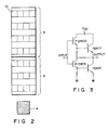
- Fig. 2 is an enlarged view showing I/O cell section 3 and input/output pad 4 shown in Fig. 1.
- a gate array a number of columns of basic cells or elements 10 for constituting basic logical circuits (gates), such as NAND, NOR, or INVERTER circuit, are arranged regularly. These elements 10 are interconnected to one another in a wiring step in accordance with the respective design required by users.
- reference numeral 5 denotes a MOS transistor region
- reference numeral 6 denotes a bipolar transistor region.
- the input/output circuit according to the invention comprises a BiCMOS which includes a bipolar transistor and a MOS transistor.
- An inverter circuit is shown in Fig.
- MOS transistor region and the bipolar transistor region include not only a MOS transistor and a bipolar transistor, respectively, but also various circuit elements (for example, a diffusion resistor).
- MOS transistor region 5 and bipolar transistor region 6 are definitely separated from each other.
- bipolar transistor region 6 which generates a relatively large current is arranged nearer to input/output pad 4.
- the aluminum wire connecting the output of a bipolar transistor and pad 4 can be short.
- the large current as noise affects little the circuits arranged near the aluminum wire, and the patterning design is simple.
- Fig. 4 shows a second embodiment of the input/output circuit according to the present invention, which comprises a plurality of MOS transistor regions and bipolar transistor regions.
- MOS transistor region 51, bipolar transistor region 61, MOS transistor region 52, and bipolar transistor region 62 are separated from and a
- Bipolar transistor region 62 includes a bipolar transistor which generates a relatively large current. Hence, the bipolar transistor can be positioned far from those portions of MOS transistor regions 51 and 52 in which a latch-up phenomenon is easy to occur, thereby preventing a latch-up phenomenon.
- the input/output circuit is constituted by a gate array, since the above-mentioned regions are aligned with one another, regular interconnection can be achieved with simple patterning. Also in this embodiment, the region nearest to the input/output pad 4 is the bipolar transistor region, resulting in the same effect as in the first embodiment.
Landscapes
- Semiconductor Integrated Circuits (AREA)
- Metal-Oxide And Bipolar Metal-Oxide Semiconductor Integrated Circuits (AREA)
- Design And Manufacture Of Integrated Circuits (AREA)
Applications Claiming Priority (2)
| Application Number | Priority Date | Filing Date | Title |
|---|---|---|---|
| JP290061/89 | 1989-11-09 | ||
| JP1290061A JPH03151660A (ja) | 1989-11-09 | 1989-11-09 | 半導体集積回路装置 |
Publications (1)
| Publication Number | Publication Date |
|---|---|
| EP0427091A1 true EP0427091A1 (de) | 1991-05-15 |
Family
ID=17751283
Family Applications (1)
| Application Number | Title | Priority Date | Filing Date |
|---|---|---|---|
| EP90120788A Withdrawn EP0427091A1 (de) | 1989-11-09 | 1990-10-30 | Eingangs-/Ausgangsschaltung für eine integrierte Halbleiterschaltungsvorrichtung |
Country Status (3)
| Country | Link |
|---|---|
| EP (1) | EP0427091A1 (de) |
| JP (1) | JPH03151660A (de) |
| KR (1) | KR930010078B1 (de) |
Citations (1)
| Publication number | Priority date | Publication date | Assignee | Title |
|---|---|---|---|---|
| US4591894A (en) * | 1982-01-20 | 1986-05-27 | Tokyo Shibaura Denki Kabushiki Kaisha | Semiconductor device having a plurality of CMOS I/O cells located at the periphery of the chip arranged in a direction perpendicular to the sides of the chip |
Family Cites Families (2)
| Publication number | Priority date | Publication date | Assignee | Title |
|---|---|---|---|---|
| JPS5533185A (en) * | 1979-01-11 | 1980-03-08 | Konishiroku Photo Ind Co Ltd | Driving member releasing mechanism of rotary drum |
| JPS61269361A (ja) * | 1985-05-24 | 1986-11-28 | Hitachi Ltd | 半導体集積回路装置 |
-
1989
- 1989-11-09 JP JP1290061A patent/JPH03151660A/ja active Pending
-
1990
- 1990-10-30 EP EP90120788A patent/EP0427091A1/de not_active Withdrawn
- 1990-11-09 KR KR1019900018100A patent/KR930010078B1/ko not_active Expired - Lifetime
Patent Citations (1)
| Publication number | Priority date | Publication date | Assignee | Title |
|---|---|---|---|---|
| US4591894A (en) * | 1982-01-20 | 1986-05-27 | Tokyo Shibaura Denki Kabushiki Kaisha | Semiconductor device having a plurality of CMOS I/O cells located at the periphery of the chip arranged in a direction perpendicular to the sides of the chip |
Non-Patent Citations (2)
| Title |
|---|
| HITACHI REVIEW, vol. 38, no. 1, February 1989, pages 55-58, Tokyo, JP; S. KADONO et al.: "Superhigh-speed Bi-CMOS gate array "HG29M100/HG21T30" * |
| PATENT ABSTRACTS OF JAPAN, vol. 12, no. 314 (E-649)[3161], 25th August 1988, Tokyo, JP; & JP-A-63 080 559 (FUJI ELECTRIC CO., LTD) 11-04-1988 * |
Also Published As
| Publication number | Publication date |
|---|---|
| KR930010078B1 (ko) | 1993-10-14 |
| KR910010689A (ko) | 1991-06-29 |
| JPH03151660A (ja) | 1991-06-27 |
Similar Documents
| Publication | Publication Date | Title |
|---|---|---|
| US4945395A (en) | Semiconductor device | |
| US4827368A (en) | Semiconductor integrated circuit device | |
| EP0098163B1 (de) | Gattermatrixchip | |
| US4855803A (en) | Selectively definable semiconductor device | |
| US4766475A (en) | Semiconductor integrated circuit device having an improved buffer arrangement | |
| EP0280236A2 (de) | Verfahren zur Herstellung einer integrierten Kundenwunschschaltung mit isoliertem Gate | |
| US6222213B1 (en) | Semiconductor integrated circuit device | |
| US5300796A (en) | Semiconductor device having an internal cell array region and a peripheral region surrounding the internal cell array for providing input/output basic cells | |
| US4701777A (en) | Gate array type semiconductor integrated circuit device | |
| US5378941A (en) | Bipolar transistor MOS transistor hybrid semiconductor integrated circuit device | |
| US5019889A (en) | Semiconductor integrated circuit device | |
| KR100223352B1 (ko) | 반도체 집적 회로 장치 | |
| US5751051A (en) | Semiconductor device equipped with electrostatic breakdown protection circuit | |
| JP2937923B2 (ja) | 半導体集積回路 | |
| US5001487A (en) | Semiconductor integrated circuit device | |
| KR100226508B1 (ko) | 풀업 또는 풀다운 저항을 갖는 반도체 장치 | |
| US5066996A (en) | Channelless gate array with a shared bipolar transistor | |
| EP0427091A1 (de) | Eingangs-/Ausgangsschaltung für eine integrierte Halbleiterschaltungsvorrichtung | |
| JP2000252363A (ja) | 半導体集積回路 | |
| EP0119059B1 (de) | Integrierte Halbleiterschaltung mit Gattermatrixstruktur | |
| EP0349294A1 (de) | I/O-Zellen für integrierte Halbleiterschaltungen | |
| EP0073608B1 (de) | Integrierte Schaltungsvorrichtung in Hauptscheibentechnik und Verfahren zu ihrer Herstellung | |
| JP2926801B2 (ja) | 半導体集積装置 | |
| JP3470084B2 (ja) | 多電源半導体装置 | |
| JPH0566737B2 (de) |
Legal Events
| Date | Code | Title | Description |
|---|---|---|---|
| PUAI | Public reference made under article 153(3) epc to a published international application that has entered the european phase |
Free format text: ORIGINAL CODE: 0009012 |
|
| 17P | Request for examination filed |
Effective date: 19901030 |
|
| AK | Designated contracting states |
Kind code of ref document: A1 Designated state(s): DE FR GB |
|
| STAA | Information on the status of an ep patent application or granted ep patent |
Free format text: STATUS: THE APPLICATION HAS BEEN WITHDRAWN |
|
| 18W | Application withdrawn |
Withdrawal date: 19931208 |