EP0427164A2 - Circuit de réduction du bruit pour récepteur FM - Google Patents
Circuit de réduction du bruit pour récepteur FM Download PDFInfo
- Publication number
- EP0427164A2 EP0427164A2 EP90121109A EP90121109A EP0427164A2 EP 0427164 A2 EP0427164 A2 EP 0427164A2 EP 90121109 A EP90121109 A EP 90121109A EP 90121109 A EP90121109 A EP 90121109A EP 0427164 A2 EP0427164 A2 EP 0427164A2
- Authority
- EP
- European Patent Office
- Prior art keywords
- low
- noise reduction
- frequency signal
- frequency
- reduction circuit
- Prior art date
- Legal status (The legal status is an assumption and is not a legal conclusion. Google has not performed a legal analysis and makes no representation as to the accuracy of the status listed.)
- Withdrawn
Links
- 230000001105 regulatory effect Effects 0.000 claims description 3
- 239000003990 capacitor Substances 0.000 description 5
- 238000011038 discontinuous diafiltration by volume reduction Methods 0.000 description 4
- 230000002238 attenuated effect Effects 0.000 description 2
- 238000010586 diagram Methods 0.000 description 2
- 238000013016 damping Methods 0.000 description 1
- 239000012530 fluid Substances 0.000 description 1
- 230000007704 transition Effects 0.000 description 1
Images
Classifications
-
- H—ELECTRICITY
- H03—ELECTRONIC CIRCUITRY
- H03G—CONTROL OF AMPLIFICATION
- H03G3/00—Gain control in amplifiers or frequency changers
- H03G3/20—Automatic control
- H03G3/30—Automatic control in amplifiers having semiconductor devices
- H03G3/3052—Automatic control in amplifiers having semiconductor devices in bandpass amplifiers (H.F. or I.F.) or in frequency-changers used in a (super)heterodyne receiver
-
- H—ELECTRICITY
- H04—ELECTRIC COMMUNICATION TECHNIQUE
- H04B—TRANSMISSION
- H04B1/00—Details of transmission systems, not covered by a single one of groups H04B3/00 - H04B13/00; Details of transmission systems not characterised by the medium used for transmission
- H04B1/06—Receivers
- H04B1/10—Means associated with receiver for limiting or suppressing noise or interference
Definitions
- the invention relates to a noise reduction circuit for a frequency modulation receiver with a receiving part which converts a frequency-modulated high-frequency signal received via an antenna into a low-frequency signal in accordance with the frequency modulation.
- FM receivers have the characteristic of producing a lot of noise when there is no or only a weak reception signal nal is present.
- noise reduction circuits which operate as squelch circuits have heretofore been used.
- the essential property of the squelch circuit is that the low-frequency signal is blocked below a certain value of the reception field strength that forms the response threshold and is transmitted above this value.
- the response threshold can usually be set to a desired value.
- the conventional squelch circuits can only produce the two states "receiver muted" for a reception field strength below the response threshold or "receiver switched loud" for a reception field strength above the response threshold.
- this property of the squelch circuit leads to the uncertainty in the case of a reception field strength, which was in the range of the response threshold, whether the reception field strength from the opposite station is just below the response threshold or whether the opposite station actually does not transmit.
- Circuits for noise reduction are known which can be used instead of or in addition to the squelch circuit described above; Although such circuits require a considerable amount of components, they do not work satisfactorily.
- the object of the invention is therefore to develop a noise reduction circuit of the type mentioned at the outset with little effort in such a way that the disadvantages of the prior art described above are avoided and in particular when the received field strength fluctuates there is no unpleasant switching on and off of the low-frequency signal.
- This object is achieved by using an attenuator which continuously controls the volume of the low-frequency signal as a function of the reception field strength between a maximum value and a minimum value.
- the attenuator according to the invention brings about a reduction in the volume of the low-frequency signal and thus also in the disturbing noise.
- the receiver is not muted, but only a volume reduction.
- the transition from the maximum value of the volume of the low-frequency signal to the minimum value, that is to say from the loud to the quiet state, is fluid due to the continuous control provided according to the invention.
- the FM receiver behaves similarly to an AM receiver.
- the volume reduction according to the invention in the case of weak reception field strengths has the advantage that the high noise component is not perceived as strongly as would be the case with undiminished volume, and that the useful signal thus appears subjectively better understandable.
- the attenuator preferably controls the volume of the low-frequency signal in proportion to the reception field strength, which results in a pleasant subjective impression when reducing the volume.
- a first setting element for setting the minimum value of the volume of the low-frequency signal is connected to the attenuator, whereby the maximum attenuation of the low-frequency signal can be set to the desired level.
- the attenuator sets the volume of the low-frequency signal above a predetermined response threshold value of the received field strength to the maximum value and begins to weaken it below the response threshold value.
- the gain of the volume reduction of the reception situation can thus be adjusted.
- a second setting element for setting the response threshold value is preferably connected to the damping element.
- a particularly expedient embodiment of the invention with a low-frequency input for inputting the low-frequency signal from the receiving part, with a low-frequency output for outputting the regulated low-frequency signal to a loudspeaker and with a control voltage input for inputting a control voltage generated by the receiving part as a function of the reception field strength is characterized in that that the attenuator contains a first resistor connected between the low-frequency input and the low-frequency output and a transistor which is connected with its base to the control voltage input and with its collector-emitter path between the low-frequency output and the ground so that the collector-emitter path increases with increasing Reception field strength becomes high-resistance.
- the invention is particularly simple to implement with this circuit and without great effort, since essentially only the transistor is used as an attenuator, the collector-emitter path of which, together with the resistor, forms a voltage divider.
- a second resistor is connected to the line connecting the low frequency output via the collector-emitter path of the transistor to the ground. Without this second resistor, the volume of the low-frequency signal would namely be reduced to zero if the transistor was completely switched on, that is to say its collector-emitter path was completely conductive, since the low-frequency output would then be short-circuited to ground.
- the second resistor causes a voltage drop between the low-frequency output and ground even when the transistor is completely switched on and thus prevents a short circuit, as a result of which the volume of the low-frequency signal is not completely at zero, but instead is only reduced to a minimum value greater than zero.
- the receiver is not switched off completely, but switched to a quiet state.
- this second resistor an attenuation of the volume of the low-frequency signal is generated, but not complete muting.
- the second resistor for setting the minimum value or the maximum attenuation of the volume of the low-frequency signal is preferably a potentiometer.
- control voltage is a positive DC voltage proportional to the reception field strength and the transistor is a pnp transistor and with its emitter via a third resistor at a reference voltage input, at which a constant positive DC voltage is present, and is connected to ground via a fourth resistor.
- the third and fourth resistors form a voltage divider, by means of which the emitter of the transistor is raised to a response voltage which is more positive than the control voltage applied to the base at low reception field strengths. The consequence of this is that the collector-emitter path of the transistor is switched through at low reception field strengths and thus a low control voltage, and the volume of the low-frequency signal is accordingly reduced.
- the collector-emitter path becomes more resistive until the transistor blocks when the control voltage is at the base is higher than the response voltage at the emitter.
- the response voltage at the emitter thus generates a response threshold below which the volume of the low-frequency signal is reduced to a minimum value, possibly zero, and above which the volume of the low-frequency signal rises to the maximum value in proportion to the control voltage.
- the fourth resistor is preferably a potentiometer for setting the response threshold.
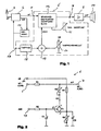
- FIG 1 shows the block diagram of an FM receiver.
- Frequency-modulated high-frequency signals HF are received via an antenna 2 and fed to a receiving part 4.
- the high-frequency signals HF are converted into low-frequency signals NF according to the frequency modulation and fed to a low-frequency input 5 of a noise reduction circuit 6.
- the noise reduction circuit 6 is shown in Figure 1 as a dashed box.
- the low frequency signal NF is fed from a low frequency output 7 of the noise reduction circuit 6 to a loudspeaker 10 via an amplifier 8.
- the receiving part 4 In addition to the low-frequency signal NF, the receiving part 4 also generates a control voltage AGC, which can consist of a positive DC voltage and is proportional to the received field strength of the received high-frequency signal HF.
- the control voltage AGC is amplified in an AGC amplifier 12 and fed to the receiving part 4 and to the noise reduction circuit 6 via a control voltage input 17.
- a voltage-controlled attenuator 14 is connected between the low-frequency input 5 and the low-frequency output 7 within the noise reduction circuit 6.
- An adjusting member 16 for adjusting the maximum attenuation of the low-frequency signal NF is connected to the attenuator 14.
- the control voltage AGC is fed from the control voltage input 17 to the attenuator via a low-pass filter 18.
- a node 19 is provided between the low-pass filter 18 and the attenuator 14, to which an adjusting element 20 for setting a response threshold value of the control voltage AGC is connected.
- the attenuator 14 continuously controls the volume of the low-frequency signal NF between a maximum value and a minimum value.
- the low-frequency signal NF is transmitted to the loudspeaker 10 without loss when regulated to the maximum value.
- the minimum value can be set with the aid of the setting element 16, as a rule between zero and a value above it. It is useful if the control voltage AGC is proportional to the received field strength of the radio frequency signal HF; however, this is not absolutely necessary.
- the attenuator 14 begins to attenuate the low-frequency signal NF.
- This received field strength value forms a response threshold and lies in low ranges of the received field strength.
- the response threshold can be set with the aid of the setting controller 20.
- FIG. 2 shows a concrete structure of the noise reduction circuit 6.
- a resistor R1 is connected between the low-frequency input 5 and the low-frequency output 7.
- a potentiometer R3 is connected, which is connected to the collector C of a pnp transistor T1 via an isolating capacitor C2.
- the control voltage input 17 is connected to the base B of the transistor T1 via a low-pass filter consisting of a resistor R2 and a capacitor C1.
- the emitter E of the transistor T1 is connected to ground both via a resistor R4 with a reference voltage input 22, to which a constant positive DC voltage UB is present, and via a potentiometer R5 and a capacitor C3 connected in parallel with it.
- the potentiometer R5 is bridged in terms of AC voltage by the capacitor C3, the resistor R1 and the series circuit comprising the potentiometer R3 and the collector-emitter path CE of the transistor T1 form an AC voltage divider for the low-frequency signal NF in the low-frequency branch.
- the collector-emitter path CE of the transistor T1 forms a variable resistor.
- the resistors R4 and R5 form a DC voltage divider, whereby the voltage at the emitter E is reduced in accordance with the ratio of the two resistance values to the reference voltage UB.
- the control voltage AGC is proportional to the received field strength. If the control voltage is more negative than the voltage at the emitter E by at least the required base-emitter voltage, the transistor T1 switches through and the collector-emitter path CE has a low resistance. In this state, the low-frequency signal NF is attenuated the most. The maximum attenuation of the low-frequency signal NF can be set using the potentiometer R3. If the difference between the control voltage AGC applied to the base B and the emitter voltage becomes smaller than the minimum base-emitter voltage required for switching on the transistor T1 and the control voltage AGC increases further, the collector-emitter path CE becomes of transistor T1 increasingly high impedance. The result of this is that the low-frequency signal NF at the low-frequency output 7 becomes louder. The emitter voltage thus forms a response threshold voltage, the level of which can be set using the potentiometer R5.
- FIGS. 1 and 2 The comparison between FIGS. 1 and 2 reveals that the attenuator 14 essentially consists of the resistor R1 and the transistor T1, the adjusting regulator 16 from the adjustable resistor R3, the low-pass filter 18 from the resistor R2 and the capacitor C1 and the adjusting regulator 20 from the contradictions stands R4 and R5 is formed.
- potentiometer R3 can also be omitted and R5 can also be constant.
- the voltage divider R4 / R5 can also be dispensed with if the reference voltage in the required amount is applied directly to the emitter E of T1.
- the volume reduction can lead to very low volumes, which would hardly be audible, so that in these cases it may be more appropriate to mute the volume.
- the function of the conventional squelch circuit namely the muting of the receiver, is thus integrated into the noise reduction circuit according to the invention. This has proven to be useful and useful, especially when using the noise reduction circuit in radio equipment.
Landscapes
- Engineering & Computer Science (AREA)
- Computer Networks & Wireless Communication (AREA)
- Signal Processing (AREA)
- Noise Elimination (AREA)
Applications Claiming Priority (2)
| Application Number | Priority Date | Filing Date | Title |
|---|---|---|---|
| DE3936888 | 1989-11-06 | ||
| DE19893936888 DE3936888C1 (fr) | 1989-11-06 | 1989-11-06 |
Publications (2)
| Publication Number | Publication Date |
|---|---|
| EP0427164A2 true EP0427164A2 (fr) | 1991-05-15 |
| EP0427164A3 EP0427164A3 (en) | 1992-05-27 |
Family
ID=6392955
Family Applications (1)
| Application Number | Title | Priority Date | Filing Date |
|---|---|---|---|
| EP19900121109 Withdrawn EP0427164A3 (en) | 1989-11-06 | 1990-11-05 | Noise reduction circuit for fm receiver |
Country Status (2)
| Country | Link |
|---|---|
| EP (1) | EP0427164A3 (fr) |
| DE (1) | DE3936888C1 (fr) |
Cited By (2)
| Publication number | Priority date | Publication date | Assignee | Title |
|---|---|---|---|---|
| EP0696852A3 (fr) * | 1994-08-11 | 1997-07-16 | Pioneer Electronic Corp | Récepteur FM |
| DE19610455A1 (de) * | 1996-03-16 | 1997-10-16 | Corcom Communication Gmbh | Verfahren und Schaltungsanordnung für ein Rausch- und Störpegeleliminationssystem |
Family Cites Families (6)
| Publication number | Priority date | Publication date | Assignee | Title |
|---|---|---|---|---|
| DE1282746B (de) * | 1966-10-27 | 1968-11-14 | Telefunken Patent | Empfaenger fuer frequenz-, phasen- oder amplitudenmodulierte Schwingungen mit einer Krachsperre |
| US3828267A (en) * | 1972-05-27 | 1974-08-06 | Sony Corp | Muting circuit |
| JPS4979762A (fr) * | 1972-12-09 | 1974-08-01 | ||
| US4016481A (en) * | 1975-11-26 | 1977-04-05 | Gte Automatic Electric Laboratories Incorporated | Unmatched field effect transistors providing matched voltage-controlled resistances |
| JPS6165518A (ja) * | 1984-09-06 | 1986-04-04 | Clarion Co Ltd | Local/dx切換回路 |
| MX161741A (es) * | 1987-08-28 | 1990-12-20 | Motorola Inc | Sistema mejorado de comunicaciones de frecuencia modulada |
-
1989
- 1989-11-06 DE DE19893936888 patent/DE3936888C1/de not_active Expired - Lifetime
-
1990
- 1990-11-05 EP EP19900121109 patent/EP0427164A3/de not_active Withdrawn
Cited By (3)
| Publication number | Priority date | Publication date | Assignee | Title |
|---|---|---|---|---|
| EP0696852A3 (fr) * | 1994-08-11 | 1997-07-16 | Pioneer Electronic Corp | Récepteur FM |
| DE19610455A1 (de) * | 1996-03-16 | 1997-10-16 | Corcom Communication Gmbh | Verfahren und Schaltungsanordnung für ein Rausch- und Störpegeleliminationssystem |
| DE19610455C2 (de) * | 1996-03-16 | 1998-06-04 | Corcom Communication Gmbh | Rauschsperre zur digitalen Ausblendung von Rauschsignalen und Störpegeln |
Also Published As
| Publication number | Publication date |
|---|---|
| EP0427164A3 (en) | 1992-05-27 |
| DE3936888C1 (fr) | 1991-05-23 |
Similar Documents
| Publication | Publication Date | Title |
|---|---|---|
| DE69131074T2 (de) | Automatischer verstärkungsregelschaltkreis mit hoher dynamik | |
| DE69131230T2 (de) | Lineare verstärkungsregelung eines verstärkers | |
| DE69529395T2 (de) | Leistungsverstärker mit grosser Dynamik | |
| DE19910371B4 (de) | Empfänger mit automatischer Hochfrequenzsignal-Verstärkungssteuerschaltung | |
| CH644974A5 (de) | Schaltungsanordnung zum selbsttaetigen anpassen der lautstaerke mindestens eines lautsprechers an einen am lautsprecherort herrschenden stoergeraeuschpegel fuer rundfunkempfaenger. | |
| DE19653558C2 (de) | Schaltung zur verzögerten automatischen Verstärkungsregelung | |
| DE2909520A1 (de) | Schaltungsanordnung zur daempfung von stoergeraeuschen | |
| DE2530144A1 (de) | Verstaerker mit veraenderbarem uebertragungsmass, insbesondere fuer ein kompander-system | |
| DE2942331A1 (de) | Schaltungsanordnung zum selbsttaetigen einstellen der lautstaerke eines lautsprechers in abhaengigkeit gon einem am lautspreherort herrschenden stoergeraeuschpegel | |
| DE60034182T2 (de) | Übertragungsschaltung und Radioübertragungsvorrichtung | |
| DE3009904C2 (de) | Schaltungsanordnung zur Kompensierung der Verstärkung eines Transistors gegen Temperaturänderungen | |
| DE3019145C2 (fr) | ||
| EP0427164A2 (fr) | Circuit de réduction du bruit pour récepteur FM | |
| EP0069843B2 (fr) | Amplificateur BF pour un récepteur de télévision | |
| DE2615383A1 (de) | Avr-empfaenger | |
| DE69715750T2 (de) | Spannungsgesteuerte Oszillatorschaltung | |
| DE3045722C2 (de) | Schaltungsanordnung zur selbsttätigen Lautstärkesteuerung von Tonsignalen bei Tonwiedergabegeräten | |
| DE3418037A1 (de) | Schaltung zur daempfung der stoerungen in einem funkempfaenger durch verwendung eines tiefpassfilters mit einstellbarem durchlassbereich | |
| DE3017781C2 (fr) | ||
| EP0456321B1 (fr) | Circuit comprenant une caractéristique de transfert commandée | |
| DE3327107C2 (de) | Hochfrequenzverstärkerschaltung | |
| DE69423808T2 (de) | Audioverstärkeranordnung | |
| DE3329663A1 (de) | Mehrstufiges signaluebertragungssystem | |
| DE69616418T2 (de) | Pegelregelungsschaltung für Empfänger | |
| DE3728327A1 (de) | Automatische pegelsteuerschaltung |
Legal Events
| Date | Code | Title | Description |
|---|---|---|---|
| PUAI | Public reference made under article 153(3) epc to a published international application that has entered the european phase |
Free format text: ORIGINAL CODE: 0009012 |
|
| AK | Designated contracting states |
Kind code of ref document: A2 Designated state(s): AT BE CH DE DK ES FR GB GR IT LI LU NL SE |
|
| PUAL | Search report despatched |
Free format text: ORIGINAL CODE: 0009013 |
|
| AK | Designated contracting states |
Kind code of ref document: A3 Designated state(s): AT BE CH DE DK ES FR GB GR IT LI LU NL SE |
|
| STAA | Information on the status of an ep patent application or granted ep patent |
Free format text: STATUS: THE APPLICATION HAS BEEN WITHDRAWN |
|
| 18W | Application withdrawn |
Withdrawal date: 19920610 |
|
| R18W | Application withdrawn (corrected) |
Effective date: 19920606 |