EP0429310A2 - Nullstromkommutierungs-Durchfluss-Leistungswandlung - Google Patents
Nullstromkommutierungs-Durchfluss-Leistungswandlung Download PDFInfo
- Publication number
- EP0429310A2 EP0429310A2 EP19900312748 EP90312748A EP0429310A2 EP 0429310 A2 EP0429310 A2 EP 0429310A2 EP 19900312748 EP19900312748 EP 19900312748 EP 90312748 A EP90312748 A EP 90312748A EP 0429310 A2 EP0429310 A2 EP 0429310A2
- Authority
- EP
- European Patent Office
- Prior art keywords
- switching device
- capacitor
- load
- voltage
- further characterised
- Prior art date
- Legal status (The legal status is an assumption and is not a legal conclusion. Google has not performed a legal analysis and makes no representation as to the accuracy of the status listed.)
- Granted
Links
Images


Classifications
-
- H—ELECTRICITY
- H02—GENERATION; CONVERSION OR DISTRIBUTION OF ELECTRIC POWER
- H02M—APPARATUS FOR CONVERSION BETWEEN AC AND AC, BETWEEN AC AND DC, OR BETWEEN DC AND DC, AND FOR USE WITH MAINS OR SIMILAR POWER SUPPLY SYSTEMS; CONVERSION OF DC OR AC INPUT POWER INTO SURGE OUTPUT POWER; CONTROL OR REGULATION THEREOF
- H02M3/00—Conversion of DC power input into DC power output
- H02M3/22—Conversion of DC power input into DC power output with intermediate conversion into AC
- H02M3/24—Conversion of DC power input into DC power output with intermediate conversion into AC by static converters
- H02M3/28—Conversion of DC power input into DC power output with intermediate conversion into AC by static converters using discharge tubes with control electrode or semiconductor devices with control electrode to produce the intermediate AC
- H02M3/325—Conversion of DC power input into DC power output with intermediate conversion into AC by static converters using discharge tubes with control electrode or semiconductor devices with control electrode to produce the intermediate AC using devices of a triode or a transistor type requiring continuous application of a control signal
- H02M3/335—Conversion of DC power input into DC power output with intermediate conversion into AC by static converters using discharge tubes with control electrode or semiconductor devices with control electrode to produce the intermediate AC using devices of a triode or a transistor type requiring continuous application of a control signal using semiconductor devices only
- H02M3/33538—Conversion of DC power input into DC power output with intermediate conversion into AC by static converters using discharge tubes with control electrode or semiconductor devices with control electrode to produce the intermediate AC using devices of a triode or a transistor type requiring continuous application of a control signal using semiconductor devices only of the forward type
- H02M3/33546—Conversion of DC power input into DC power output with intermediate conversion into AC by static converters using discharge tubes with control electrode or semiconductor devices with control electrode to produce the intermediate AC using devices of a triode or a transistor type requiring continuous application of a control signal using semiconductor devices only of the forward type with automatic control of the output voltage or current
-
- H—ELECTRICITY
- H02—GENERATION; CONVERSION OR DISTRIBUTION OF ELECTRIC POWER
- H02M—APPARATUS FOR CONVERSION BETWEEN AC AND AC, BETWEEN AC AND DC, OR BETWEEN DC AND DC, AND FOR USE WITH MAINS OR SIMILAR POWER SUPPLY SYSTEMS; CONVERSION OF DC OR AC INPUT POWER INTO SURGE OUTPUT POWER; CONTROL OR REGULATION THEREOF
- H02M3/00—Conversion of DC power input into DC power output
- H02M3/22—Conversion of DC power input into DC power output with intermediate conversion into AC
- H02M3/24—Conversion of DC power input into DC power output with intermediate conversion into AC by static converters
- H02M3/28—Conversion of DC power input into DC power output with intermediate conversion into AC by static converters using discharge tubes with control electrode or semiconductor devices with control electrode to produce the intermediate AC
- H02M3/325—Conversion of DC power input into DC power output with intermediate conversion into AC by static converters using discharge tubes with control electrode or semiconductor devices with control electrode to produce the intermediate AC using devices of a triode or a transistor type requiring continuous application of a control signal
- H02M3/335—Conversion of DC power input into DC power output with intermediate conversion into AC by static converters using discharge tubes with control electrode or semiconductor devices with control electrode to produce the intermediate AC using devices of a triode or a transistor type requiring continuous application of a control signal using semiconductor devices only
- H02M3/33569—Conversion of DC power input into DC power output with intermediate conversion into AC by static converters using discharge tubes with control electrode or semiconductor devices with control electrode to produce the intermediate AC using devices of a triode or a transistor type requiring continuous application of a control signal using semiconductor devices only having several active switching elements
- H02M3/33576—Conversion of DC power input into DC power output with intermediate conversion into AC by static converters using discharge tubes with control electrode or semiconductor devices with control electrode to produce the intermediate AC using devices of a triode or a transistor type requiring continuous application of a control signal using semiconductor devices only having several active switching elements having at least one active switching element at the secondary side of an isolation transformer
Definitions
- This invention relates to zero-current switching, forward power conversion.
- One such power converter scheme transfers energy from a voltage source for delivery to a load using a transformer that has a controlled amount of effective secondary leakage inductance (e.g. a leakage reactance transformer).
- a transformer that has a controlled amount of effective secondary leakage inductance (e.g. a leakage reactance transformer).
- a switch On the source side of the transformer, a switch is connected in series with the source and the primary winding of the transformer. The switch connects the source to and disconnects it from the primary winding in a succession of energy transfer cycles.
- a first unidirectional conducting device and a capacitor are connected in series with the secondary winding.
- the capacitor and the effective leakage inductance define a characteristic time scale for the cycling of the switch such that the switch is cycled on and off at times when the current in the switch and the first unidirectional conducting device are essentially zero.
- the first unidirectional conducting device constrains current flow in the effective leakage inductance to be directed only in the direction of the load, thereby preventing bidirectional energy flow (resonance) from occurring between the effective leakage inductance and the capacitor.
- Energy is transferred to the load via a second inductor whose value is large in comparison with the effective leakage inductance. This second inductor effectively appears as a current sinking load across the capacitor.
- a second unidirectional conducting device connected in parallel with the capacitor constrains the capacitor voltage to be unipolar and prevents bidirectional energy transfer from occurring between the second inductor and the capacitor.
- the parameters of the circuit elements and the requirement of zero-current switching constrain the converter to unidirectionally transfer a fixed amount of energy during every energy transfer cycle. Because the output power is the product of that fixed amount of energy multiplied by the frequency of occurrence of the energy transfer cycles, control of the output power requries varying the frequency of the energy transfer cycles.
- the prior art topology allows implementation of converters which achieve power densities and efficiencies unachievable with either "non-zero-current switching" topologies or contemporary “resonant” topologies.
- the invention is a zero-current switching converter in which the amount of energy transferred during a given energy transfer cycle may be selectively governed.
- the invention features the combination of a voltage source; a power transformer including a primary and a secondary winding, the power transformer being constructed to have an effective secondary leakage inductance L2e; a first switching device connected to selectively couple the power source across the primary winding of the power transformer; a first unidirectional conducting device connected in series with the secondary winding and oriented to conduct during conduction by the first switching device; a capacitor of capacitance C connected in series with the secondary winding and the first unidirectional conducting device; a controller having means for selectively closing and opening the first switching device to transfer power from the voltage source via the effective leakage inductance of the transformer to charge the capacitance during an energy transfer cycle having a characteristic time scale of ⁇ ⁇ L2e*C ; and a second switching device connected on the secondary side of the transformer; the controller including a second control means for opening and closing the second switching device to selectively govern the amount of energy transferred during the energy transfer cycle.
- the second switching device may be connected in parallel with the capacitor to prevent charging of the capacitor when the second switching device is closed.
- An inductor is connected in series between the capacitor and a load to deliver current to the load.
- the second control means includes means for detecting closure of the first switching device, means for opening the second switching device at substantially the same time that the first switching device is closed, means for detecting voltage across the capacitor, and means for closing the second switching device when voltage across the capacitor is substantially zero.
- the converter circuit delivers power to two or more independent loads and for that purpose includes a primary inductor connected in series with the capacitor and one of the independent loads, and a plurality of secondary windings magnetically coupled to the primary inductor, the secondary windings respectively having relative numbers of turns that correspond to the relative voltages to be delivered respectively to the independent loads.
- the secondary winding is connected to one of the independent loads via a subcircuit that includes a secondary unidirectional conducting device oriented to conduct current when the voltage across the primary inductor is positive in a direction between the load and the capacitor.
- Each subcircuit includes a filter element for smoothing the voltage across the independent load.
- the filter element may include a capacitor in parallel with the load.
- each subcircuit comprises a post-regulator for regulating the voltage delivered to the independent load.
- the secondary windings may be loosely coupled to the primary inductor.
- the post-regulator may comprise a rest magnetic amplifier or a dissipative regulator.
- the second switching device may consist of a switch capable of unidirectional conduction when closed connected in a parallel with a second unidirectional conduction device, the switch and second unidirectional conducting device being oriented to conduct in opposite directions. This second switching device would be oriented so that said second unidirectional conducting device will prevent charging of said capacitor when current flowing in said second inductor is in a direction towards the load.
- the second switching device may be connected in parallel with the secondary winding of the power transformer.
- a second unidirectional conducting device may be connected in parallel with the capacitor, oriented to prevent charging of the capacitor when current flowing in the second inductor is in a direction towards the load.
- An inductor is connected between the capacitor and the load.
- the second control means may include means for detecting closure of the first switching device, and means for opening the second switching device at a selected time thereafter.
- the invention features operating some embodiments of the converter circuit in a reverse boost mode by closing the second switching device when the voltage across the capacitor is substantially zero to prevent reverse current in the inductor from transferring energy to the capacitor.
- the second switching device is opened at substantially the same time that the first switching device is closed.
- the frequency at which the first switch is opened and closed is varied to effect output voltage regulation.
- the converter circuit is operated in a forward boost mode by holding the second switching device closed for a selected period of time after the first switching device has been closed.
- the second switching device is closed when voltage across the capacitor is substantially zero.
- the frequency at which the first switch is opened and closed is varied to effect output voltage regulation when the ratio of the value of the voltage source to the value of the output voltage of the converter is greater than the ratio of the number of turns on the primary of the power transformer to the number of turns on the secondary of the power transformer.
- the time period during which the second switching device remains closed is controlled so as to maintain the output voltage of the converter circuit in regulation irrespective of the relative values of the voltage source and the output voltage.
- the invention features controlling the converter circuit (in which the ratio of the number of turns on the primary of the power transformer to the number of turns on the secondary of the power transformer is greater than the ratio of the maximum value of the voltage source to the value of the output voltage of the converter) to operate in a forward boost mode, in which the second switching device is held closed for a selected period of time after the first switching device has been closed.
- the second switching device is closed when voltage across the capacitor is substantially zero.
- the opening and closing of the first switching device occurs at constant frequency. The time period during which the second switching device remains closed is controlled so as to maintain the output voltage of the converter circuit in regulation.
- the voltage source has a possibly varying voltage level
- the second switching device is opened when the level of current flowing in the first unidirectional conduction device rises to become equal to the level of current flowing in the direction of the load in the second inductor so long as the voltage level does not fall below a predetermined value, and is otherwise controlled to stay closed for a longer time period to maintain the output voltage of the converter circuit in regulation.
- the opening and closing of the first switching device is permitted to occur at frequencies within a predetermined frequency band.
- the forward boost mode provides a mechanism for selectively increasing the amount of energy transferred per converter operating cycle, irrespective of the relative values of converter input and output voltage.
- forward boost allows implementing converters which maintain the output voltage in regulation as output power is varied, yet which operate either at a constant, relatively high, frequency or within a narrow band of relatively high frequencies.
- the reverse boost mode eliminates the cause of the "discontinuous mode" in the prior art converter. If the second switching device is opened at essentially the same time that the first switching device is closed, forward energy transfer per cycle will be reduced as power output is reduced and output voltage may be regulated while operating the converter within a relatively narrow range of relatively high frequencies.
- Reverse boost also allows another embodiment where multiple auxiliary windings on the second inductor may be used to generate a multitude of regulated outputs, each one of which would remain in regulation as loads on the various outputs are independently varied.
- the voltages generated by the auxiliary windings will be related to the main output voltage by the ratio of the number of turns on any particular auxiliary winding to the number of turns on the main winding.
- energy transferred to the various auxiliary loads is not limited to the magnetic energy stored in the second inductor at the time that the auxiliary unidirectional conducting devices start conduction but may also be sourced from energy storage elements which form part of the main output load (i.e. filter capacitors).
- Embodiment of enhanced zero-current switching topology described in more detail below more closely approach an "ideal" power conversion topology by providing: A means for maintaining output voltage regulation, while power output is varied, while operating either at a constant, relatively high, frequency, or within a narrow band of relatively high frequencies; A mean for controlling the effects of current reversal in the second inductor, thereby eliminating the "discontinuous mode", and allowing reduction in the value of the second inductor to a value consistent with other desirable performance goals; A means for easily generating a multitude of regulated outputs, each one of which would remain in regulation as loads on the various outputs are independently varied; A means for reducing the value of input voltage required to maintain output voltage regulation while power output is varied; A means for further improving power density by increasing power output without increasing maximum operating frequency, while simultaneously allowing reduction both in the inductance value and the physical size of the second inductor; The benefits achieved with the underlying zero-current switching forward converter.
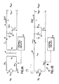
- Figure 1A is a schematic of an embodiment of a zero-current switching power converter of the kind described in U. S. Patent No. 4,415,959 (referred to hereafter as the "prior art converter").
- Figure 1B is a schematic of the prior art converter where the input source 12, leakage reactance transformer 14, and the first switch 26, are replaced by a model consisting of an effective inductance 114, of value L2e, representing the effective secondary leakage inductance of leakage reactance transformer 14, a transformed input source 112 whose voltage value, Veq, is the value of input source 12, Vin, multiplied by the secondary-to-primary turns ratio of transformer 14, and a first switch 26.
- Equation 2 requires: Iout/I1 ⁇ 1 (3) Since, from Equation 1: Veq ⁇ Vout*Iout/I1 then, Veq ⁇ Vout. Said another way, by constraining the average current I2 to a range of positive values only, the behaviour of the second unidirection conducting device 18 limits the prior art converter to operating only in a "buck" mode (i.e. for Veq > Vout).
- the behavior of the second unidirection conducting device 18 in the prior art converter is also responsible for the dependence of output power on operating frequency.
- closure of the first switching device 26 impresses the transformed input source voltage Veq across the effective inductance 114, whose initial instantaneous current, I1, is zero.
- a positive ramp of current I1 will flow in the effective inductance 114 until the current in the second unidirectional conducting device 18 (i.e. the difference between the instantaneous current in the effective inductance 114 and the instantaneous current in the second inductor 24, Iout), becomes zero, at which time the second unidirectional conducting device 18 ceases conducting.
- Ls L2e + L
- the second unidirectional conducting device 18 ceases conducting when the values of I1 and Iout are equal.
- the values of Ip and Ic are also equal, and Equations 4 and 4a reduce to:
- the second unidirectional conducting device 18 prevents energy stored in the second inductor 24 from being transferred to the capacitor during the last phase of the converter operating cycle when the capacitor voltage is zero and positive current Iout flow in the second inductor 24. Stated another way, the second unidirectional conducting device 18 prevents energy transfer to the capacitor 20 so long as the second inductor 24 is transferring energy to the load. However, below some value of load, current reversal in the second inductor cannot be prevented.
- a preferred embodiment of a zero-current switching power converter 50 is modified from the prior art converter 10 so that: Vout may be regulated even when Vin decreases to a value less than Vout (i.e. to a level at which the average value of I2 would have to go negative to support Vout); the amount of forward energy, E, transferred during each cycle, may be varied, thereby allowing Pout to be controlled without changing the operating frequency of the converter; both reverse energy transfer from the load to the capacitor, and forward energy transfer from the source to the capacitor may be simultaneously controlled, thereby eliminating the "discontinuous: mode of operation and allowing a mode of operation whereby the output voltage may be regulated as Pout varies while the converter operates over a relatively narrow range of high frequencies.
- second switch 28 capable of bidirectional conduction, replaces the second unidirectional conducting device 18 of Figure 1A.
- a voltage source 12 is coupled to the primary winding of a leakage reactance transformer 14 via a first switch 26.
- First switch 26 is cycled on and off by a control circuit 22.
- Second switch 28 is cycled on and off by controller 32.
- Control circuit 22 and controller 32 may be parts of a single controller.
- a first unidirectional conducting device 16 and a capacitor 20 are connected in series with the secondary winding of leakage reactance transformer 14.
- the second switch 28 is connected across the capacitor 20.
- a second inductor 24 is connected in series between the capacitor 20 and the load.
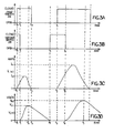
- Figures 3A - 3D show the waveforms of the converter 150 operating in a mode referred to as Forward Boost mode.
- the first switch 26 is closed by control circuit 22, initiating a converter operating cycle.
- the transformed input source 112 causes a positive, linearly increasing, current I1, to start flowing in the effective inductance 114.
- the second switch is closed, current I1 flows through the first unidirectional conducting device 16 and second switch 28, and returns to the transformed input source, thus storing energy in the effective inductance 114.
- this first phase of the converter cycle would end when the instantaneous value of current I1 became equal to the instantaneous value of current Iout, at which point the second unidirectional conducting device 18 ( Figure 1B) would cease conducting, and energy transfer to the capacitor 20 and load would commence.
- the controller 32 holds the second switch 28 closed long enough to allow the instantaneous value of current I1 to increase beyond the instantaneous value of Iout (i.e.
- the second switch 28, of Figure 2 provides a mechanism for increasing the average current I1 to values which are greater than the average value of the current Iout.
- this allows maintaining output voltage in regulation, as power is varied, for values of transformed input source 112, Veq, which are less than the regulated output voltage, Vout.
- Forward Boost provides a mechanism for overcoming the "dropout voltage" limitation of the prior art converter.
- Equation 4 will again describe the behaviour of the capacitor voltage during this phase, using values for Ip and Io which correspond to the instantaneous values of I1 and Iout when the second switch opens.
- the peak voltage on the capacitor (Vcl, at time t2 in Fig. 3D) in the converter of Figure 2B will also depend on the difference in the current I1 and Iout at the time that the second switch 28 is opened.
- the converter of Figure 2B can "boost" its forward energy transfer to values greater than that which can be transferred by the prior art converter of Figure 1B, and can furthermore regulate the degree of Forward Boost within a continuous range of energy values by regulating the time period t0 to t1.
- the boosted peak value, Vcl, of capacitor voltage, Vc, and the boosted peak value of Ia, of the current I1, in Figs. 3C and 3D, will therefore be greater than the corresponding peak values which would be found in a prior art converter, all other circuit elements being equal.
- the forward energy transfer phase is followed by a period during which energy stored in the capacitor 20 is, via the medium of the second inductor 24, delivered to the load.
- the current I1 returns to zero and the first switch 26 is turned off.
- the capacitor 20 voltage decays to zero as its stored energy is delivered to the load by the positive current Iout.
- second switch 28 is closed, preventing positive current flow in the second inductor 24 from reverse charging the capacitor 20.
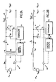
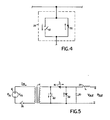
- An alternate embodiment of the present invention implements the second switch 28, of Figure 2, with the circuit arrangement of Figure 4.
- the circuit is comprises of a second unidirectional conducting device 50 connected across a unidirectional switch 52, such that the preferred directions of conduction of the two devices are in opposition (as indicated by the arrows adjacent to the two devices).
- the unidirectional switch 52 might be a bipolar or a MOSFET transistor. Utilizing this circuit allows the benefits of Forward Boost to be obtained without compromise.
- the second unidirectional conducting device 50 will conduct positive current I2 until the current passes through zero, at which point the unidirectional switch 52 will smoothly take over conduction of negative current flow. It should be noted that if the unidirectional switch 52 is opened prior to the current I2 going negative, the presence of the second unidirectional conducting device 50 will cause operation to revert to that of a prior art converter.
- the topology of the present invention may be used to selectively regulate the amount of forward energy transferred during a converter operating cycle, irrespective of the relative values of the transformed input source 12 and the regulated output voltage, Vout.
- an appropriate controller 32 which may be a part of control circuit 22
- many possible converter operating modes can be realized which exploit this mechanism.
- embodiments of circuit in accordance with the present invention might be used solely to provide reduced input operating voltage capability during transient periods of severe input source "brownout".
- the second switch circuit 28, of Figure 4 would be incorporated into the topology of Figure 2, but the unidirectional switch 52 would be maintained in its off state until the converter input voltage dropped below some predetermined level, Vmin.
- Vmin some predetermined level
- the converter will operate as a prior art converter and provide all the benefits of the prior art topology.
- Forward Boost mode would be asserted and output voltage regulation would be maintained down to relatively lower values of input voltage than could otherwise be supported by the prior art topology (for example, down to 100 VDC).
- the turns ratio of the leakage reactance transformer 14 of Fig. 2A could be set to ensure that, for the maximum specified value of input source 12, the value of transformed input source voltage 112 will always be less than the desired value of regulated output voltage Vout.
- the turn-on transitions of the main switch would be controlled, by control circuits 22, to occur at a constant frequency.
- a controller 32 would be implemented which would, in response to deviations of the actual converter output voltage from the desired value of regulated output, Vout, selectively regulate the time between closure of the first switch 26 and opening of the second switch 28, thereby regulating the amount of Forward Boost asserted as a means of maintaining output voltage in regulation as output power is varied.
- some controlled degree of Forward Boost is always asserted and the output voltage will be maintained in regulation, as the load is varied, while the converter is operating at a constant frequency.
- L the value of the second inductor 24
- the high constant operating frequency in this mode reduces the time period during which the second inductor 24 must support energy transfer to the load between converter forward energy transfer cycles, and the amount of energy which needs to be stored in the second inductor 24 is reduced.
- FIG. 5 An alternate embodiment of the present invention, useful for operation in Forward Boost mode, is disclosed in Figure 5.
- a unidirectional switch 60 is connected directly across the secondary winding of the leakage reactance transformer, and a second unidirectional conducting device 62 is connected across the capacitor 20.
- this topology will exhibit slightly lower losses than the topology of Figure 2, since the first unidirectional conducting device 16 does not carry current during the Forward Boost phase of the cycle when the unidirectional switch 60 is carrying current.
- FIGS 6A - 6E show the waveforms of the converter 150 of Figure 2 operating in a mode referred to as Reverse Boost mode (at a relatively low value of Pout).
- Reverse Boost mode at a relatively low value of Pout.
- current in the second inductor 24, Iout is permitted to reverse during an operating cycle, so that at the beginning of a subsequent cycle Iout is flowing in a negative direction (i.e. from the load toward the second switching device 28).
- first switch 26 is open, and the second switching device 28 is closed.
- Negative current Iout is flowing from the load (i.e. from energy storing elements which form part of the load, such as filter capacitors) towards the second switching device 28, and is bypassed around the capacitor 20 and returned to the load via the second switching device 28.
- the value of Iout just prior to time t0 is -Ix, as shown in Figure 6D.
- the capacitor 20 voltage is at zero due to the second switching device 28 being closed. Under these conditions, if the second switching device 28 is opened at essentially the same time that the first switch 26 is closed, a Reverse Boost cycle will be initiated.
- Figure 6A and 6B the cycling of the switches is shown taking place simultaneously at time t0, resulting in immediate initiation of energy transfer from the transformed input source 112 to the capacitor 20, as shown in Figure 6C.
- the capacitor voltage during the forward energy transfer phase will be given by Equation 4, with the initial value of current Ip equal to zero, and the initial value of current Io equal to -Ix.
- the current flowing in the effective inductance 114 during the forward energy transfer phase can be shown to be: Examination of Equation 10 reveals that both the peak value of I1(t), and the time duration during which I1(t) is positive (i.e. the time period t0 to t1), are strongly dependent on the value, Ix, of negative current Iout which is flowing at time t0. This is to be expected, since, after opening the second switch 28, the negative current Ix starts to positively charge the capacitor 20. Positive voltage buildup on the capacitor 20, in response to the negative current Ix, acts to reduce the voltage across the effective inductance 114 during the energy transfer phase, thereby acting as a barrier to current flow and reducing forward energy transfer.
- Figure 7 shows waveforms of the forward current, I1(t), of Equations 11, for different values of the ratio Ir/If.
- the effect of increasing the ratio Ir/If i.e. increasing Ix
- Figure 8 shows the effect of reverse current, Ix, on forward charge transferred per cycle for a converter according to the present invention operating in Reverse Boost mode.
- Figures 7 and 8 illustrate the effect that initial reverse current flow in the second inductor 24 has upon forward energy transfer per cycle.
- the effect of initial reverse current flow in the second inductor 24 is a reduction in forward energy transferred during the cycle. Since Ix will become more negative as the average value of load current, Iout, drops, the amount of charge transferred per cycle will also drop. The result is that, for a given value of load, and all other circuit elements being equal in value, a converter operating in Reverse Boost mode must operate at a higher frequency than a prior art converter.
- Reverse Boost mode When operated in Reverse Boost mode according to the present invention can operate down to no load without the deleterious effects of "discontinuous" mode.
- Reverse Boost eliminates the source of discontinuous mode while at the same time reducing the relative range of frequencies over which the converter will operate as load is decreased.
- reducing the inductance value of the second inductor 24 is not only made possible by Reverse Boost, it is required to ensure that current reversal will occur at light loads.
- the second switching device 28 in our converter is implemented using the topology of Figure 4.
- a MOSFET transistor with an on-resistance of approximately 30 milliohms is used for switch 52, and a Schottky diode is used for the unidirectional conducting device 50.
- the value, L, of the second inductor 24 is 10 microhenries, while in our converter 50, the inductance value is reduced to 3 microhenries.
- the discontinuous mode is eliminated since the second switching device 28 prevents reverse energy transfer between the second inductor 24 and the capacitor 20.
- operation at an average output current of 1 Ampere occurs at a stable converter operating frequency of about 161 Kilohertz. This is higher than the operating frequency of the prior art converter operating at the same load because the value of the second inductor 24 has been reduced, and current reversal in the second inductor (at a value Ix of about 1.8 Amperes) is occurring in our converter at this value of load, resulting in a reduction of forward energy transferred per cycle.
- Reverse Boost would be implemented by using the circuit of Figure 4 as the second switch 28 in our converter 50 of Figure 2A.
- the value of second inductor 24 would be reduced relative to a prior art converter.
- the controller 32 would open the unidirectional switch 52 (Fig. 4) at essentially the same time that the first switch 26 was closed, and close the unidirectional switch 52 when the capacitor 20 voltage returned to zero.
- the variable frequency control circuit of the prior art converter would be used as the control circuit 22 for the first switch. At relatively high loads, the operating frequency would be relatively high, and the current in the second inductor 24 would always flow in a positive direction.
- Reverse Boost will become a self-regulating process in that the converter operating frequency will stabilize at a value such that the reverse current in the second inductor 24 at the start of a cycle (Ix of Equation 10) is sufficient to maintain the output voltage in regulation at the particular value of load.
- the lower limit on operating frequency in the Reverse Boost mode of operation will effectively be dependent upon the small amount of losses present in the circuit elements forming the output circuit.
- a value of Ix will be reached at which forward power flow will just be sufficient to compensate for output circuit losses.
- our topology may be used to selectively regulate the amount of forward energy transferred during a converter operating cycle, while simultaneously regulating reverse energy transfer from energy storing elements in the load to the capacitor 20. Elimination of the "discontinuous" operating mode at low values of load, and reduction in the range of frequencies over which the converter operates as load is reduced, are two of the resulting benefits.
- an appropriate controller 32 which may be a part of control circuit 22
- many possible converter operating modes can be realized which exploit this mechanism.
- Reverse Boost might be used solely to eliminate the discontinuous mode at light loads while raising the minimum converter operating frequency.
- Other controller implementations might utilize the topology of the present invention to assert Reverse Boost at light loads and Forward Boost at higher values of load. This could further reduce the operating frequency range of the converter while providing other benefits, discussed above.
- the converter according to the present invention may be adapted to provide a multitude of independent outputs, each one of which will remain in regulation as loads on the various outputs are varied.
- the second inductor 24 is replaced with the circuit arrangement shown in Figure 9.
- a second inductor 224 is modified to incorporate a multitude of auxiliary windings 226.
- Each auxiliary winding 226 is connected in series with a unidirectional conducting device 250, and the parallel combination of a filter capacitor 261, and a load (the loads being represented as load voltages Vl1, Vl2, ...), the unidirectional conducting devices 250 being oriented to conduct when the capacitor voltage 20 goes essentially to zero and the main regulated output voltage, Vout, is impressed in reverse across the main winding 225 of the second inductor 24.
- the voltages generated by the auxiliary windings 226 Vo1, Vo2,..., will be related to the main output voltage, Vout, by the ratio of the number of turns on any particular auxiliary winding 226, N2, to the number of turns on the main winding 225, N1.
- auxiliary output voltages in fixed ratio to the main output voltage depends upon maintaining the capacitor 20 voltage at zero throughout the time period during which energy is being transferred to the auxiliary loads (i.e. so that the voltage impressed in reverse across the main winding 225 of the second inductor 224 remains fixed at Vout). If the prior art converter 10 of Figure 1A were adapted in accordance with Figure 9, maintaining the various auxiliary outputs in regulation would require that a minimum load always be present on the main output. This is because the second unidirectional conducting device 18 ( Figure 1A) will only maintain the capacitor voltage at zero if positive current is flowing in the second inductor 24 throughout the time period during which energy is being transferred to the auxiliary loads.
- energy transferred to the various auxiliary loads is not limited to the magnetic energy stored in the second inductor 224 but may also be sourced from energy storage elements which form part of the main output load (i.e. filter capacitors).
- the converter allows a multitude of auxiliary output voltages to be maintained in a fixed ratio to the main output voltage, as loads on the various outputs are independently varied, and without requiring that a minimum load be maintained on the main converter output.
- the multiple output embodiment of converter according to the present invention is useful in many practical applications, but has characteristics which can create difficulties in others.
- the various auxiliary output voltages, Vo1, Vo2,..., ( Figure 9) are in fixed ratio to the maintain output voltage, Vout, during the period of time that the unidirectional conducting devices 250 are conducting current (assuming perfect coupling between the auxiliary winding 226 and the main winding 225), the voltages delivered to the loads, VL1, VL2,..., will be reduced in value by the voltage drop across the unidirectional conducting devices 250.
- VL1 Vo1 - Vd (14)
- Vo1 N2 N1 * Vout
- N2 is the number of turns on the auxiliary winding 226, N1 is the number of turns on the main winding 225, and Vd is the voltage drop across the unidirectional conducting device 250.
- a similar equation would apply for each of the other auxiliary outputs.
- Equations 14 and 15 since the number of turns, N1 and N2, can only have integer values, and since very large values of either N1 or N2 are impractical, the range of allowable values of Vo1 (and therefore VL1) is not continuous; the value of voltage drop in the unidirectional conducting device 250, Vd, will vary from device to device, and will also vary with changes in load and temperature. Thus, there is a limit to the degree to which an auxiliary output can be regulated. Furthermore, this limitation becomes more severe as the desired value of VL1 gets smaller since the relative contribution of the effect of variations in Vd is increased; equation 15 assumes perfect coupling between the auxiliary winding 226 and the main winding 225.
- the second inductor 24 of Figure 9 can be constructed to ensure that a small amount of effective leakage inductance was present in all of the secondary windings 226 (i.e. a "loosely coupled second-inductor" would be constructed).
- the relative turns ratios of each of the auxiliary windings 226 on the loosely coupled second-inductor 224 would be selected to ensure that the voltage outputs of the secondary windings 226 Vo1, Vo2, ..., are greater than the values of the regulated voltages VL1, VL2,..., desired at the loads.
- each auxiliary load (represented by the load voltages VL1, VL2,...) would be connected to one of the secondary windings 226 via a post-regulator 260 which would reduce the average value of each secondary voltage Vo1, Vo2,..., to the desired value of load voltage VL1, VL2,....
- each post-regulator 260 would incorporate a unidirectional conducting device 250 in the series path between the secondary winding 226 and the load, the specific placement of the unidirectional conducting device would depend on the specific post-regulation method chosen.
- a preferred embodiment of the post-regulator would be a reset magnetic amplifier (followed by a storage capacitor) which would perform the regulation function in an essentially lossless fashion.
- the simplest topology for the magnetic amplifier would incorporate a unidirectional conducting device 250 at the load side of the post-regulator 260, with a resettable inductor in series with, but interposed between, the secondary widing 226 and the unidirectional conducting device 250.
- post regulation can be achieved through use of a dissipative post-regulator 260 either with a storage capacitor at both its input and output, or with a storage capacitor at its output only.
- the unidirectional conducting devices would be connected directly to the secondary windings 226 at the input side of the post-regulators 260.
- the topology of the present invention provides a mechanism for implementing new converter operating modes (Forward Boost and Reverse Boost) which overcome many characteristic limitations of the prior art topology. It is worthwhile to consider the relative benefits of both Forward and Reverse Boost within the contexts of contemporary component technology and current power systems architecture: - Reverse Boost combines simplicity in implementation with a universally desirable set of benefits: elimination of the discontinuous operating mode at light loads, reduction in the range of converter operating frequency as load is varied, the ability to generate multiple outputs without a minimum load being required on any one output, and reduction in size of the second inductor.
- FIG. 1A A very useful and desirable feature of the prior art converter topology 10, Figure 1A, is that a multitude of similar converters may be operated in parallel, in synchronized arrays, where all converters inherently, and dynamically, share an equal portion of the power delivered to the load (i.e. as in Vinciarelli, "Power Booster Switching at Zero Current", U. S. Patent No. 4,648,020 the disclosure of which is to be regarded as incorporated herein by reference).
- Vinciarelli Power Booster Switching at Zero Current
- U. S. Patent No. 4,648,020 the disclosure of which is to be regarded as incorporated herein by reference.
- accuracy in power sharing between converters will, in part, be dependent upon the relative timing of the opening of the second switch 28 in each converter in the array. This would be a particular problem when the converters in the array are configured to operate in Forward Boost mode.
- a 5 Volt output converter which must operate with an input voltage of 350 VDC (not atypical of the rectified high line voltage from a 220 Volt line), would require a transformer turns ratio in excess of 70:1. This is not impossible, but it is difficult to implement in a small size, with low losses, at high power levels.
- Reverse Boost is a preferred operating mode because of its simplicity and universality of application. Within the context of contemporary component technology, Forward Boost is most useful where transient power boost may be required, where it can provide temporary operation during conditions of low input operating voltage, or for constant frequency operation at lower power levels. As component technology continues to improve, broader applicability of the Forward Boost mode can be anticipated.
- the topology of our converters 50 provides a mechanism for overcoming many of the characteristic limitations of the prior art topology 10, it does so without sacrificing the prior art topology's inherently low loss characteristic. Avoidance of switching losses is retained in the present invention: the first switch 26 of Figure 2 is switched on and off at zero-current, while the second switching device 28 is operated in a "zero-voltage switching" mode (i.e. at the times at which it is cycled on and off, the voltage across it is zero and cannot change instantaneously due to the presence of the capacitor 20 across it).
Landscapes
- Engineering & Computer Science (AREA)
- Power Engineering (AREA)
- Dc-Dc Converters (AREA)
- Power Conversion In General (AREA)
Applications Claiming Priority (2)
| Application Number | Priority Date | Filing Date | Title |
|---|---|---|---|
| US44088289A | 1989-11-22 | 1989-11-22 | |
| US440882 | 1989-11-22 |
Publications (3)
| Publication Number | Publication Date |
|---|---|
| EP0429310A2 true EP0429310A2 (de) | 1991-05-29 |
| EP0429310A3 EP0429310A3 (en) | 1991-10-09 |
| EP0429310B1 EP0429310B1 (de) | 1998-09-23 |
Family
ID=23750563
Family Applications (1)
| Application Number | Title | Priority Date | Filing Date |
|---|---|---|---|
| EP19900312748 Expired - Lifetime EP0429310B1 (de) | 1989-11-22 | 1990-11-22 | Nullstromkommutierungs-Durchfluss-Leistungswandlung |
Country Status (4)
| Country | Link |
|---|---|
| EP (1) | EP0429310B1 (de) |
| JP (1) | JPH082176B2 (de) |
| CA (1) | CA2029209C (de) |
| DE (1) | DE69032672T2 (de) |
Cited By (1)
| Publication number | Priority date | Publication date | Assignee | Title |
|---|---|---|---|---|
| US5291385A (en) * | 1992-04-02 | 1994-03-01 | Vlt Corporation | Zero-current switching forward power converter operating in damped reverse boost mode |
Families Citing this family (3)
| Publication number | Priority date | Publication date | Assignee | Title |
|---|---|---|---|---|
| US7269034B2 (en) | 1997-01-24 | 2007-09-11 | Synqor, Inc. | High efficiency power converter |
| EP0954899A2 (de) | 1997-01-24 | 1999-11-10 | Fische, LLC | Hocheffizienter stromrichter |
| US10199950B1 (en) | 2013-07-02 | 2019-02-05 | Vlt, Inc. | Power distribution architecture with series-connected bus converter |
Family Cites Families (11)
| Publication number | Priority date | Publication date | Assignee | Title |
|---|---|---|---|---|
| JPS5627075A (en) * | 1979-08-10 | 1981-03-16 | Nippon Kokan Kk <Nkk> | Wave-operated generation set |
| US4415959A (en) * | 1981-03-20 | 1983-11-15 | Vicor Corporation | Forward converter switching at zero current |
| JPS5944971A (ja) * | 1982-09-06 | 1984-03-13 | Fujitsu Ltd | Dc−dcコンバ−タ |
| JPS6059973A (ja) * | 1983-09-12 | 1985-04-06 | Nec Corp | スイツチングレギユレ−タ |
| JPS61295870A (ja) * | 1985-06-24 | 1986-12-26 | Hitachi Metals Ltd | 多出力dc−dcコンバ−タ |
| DE3543299A1 (de) * | 1985-12-07 | 1987-06-11 | Ceag Licht & Strom | Vorrichtung zur entmagnetisierung des transformators eines flusswandlers und verfahren zu ihrem betrieb |
| JPS6336187U (de) * | 1986-08-25 | 1988-03-08 | ||
| FR2608857B1 (fr) * | 1986-12-19 | 1989-05-12 | Sodilec Sa | Convertisseur continu-continu du type " forward " a commutation a courant nul et a fonctionnement en courants bidirectionnels |
| JPH0740784B2 (ja) * | 1987-02-04 | 1995-05-01 | 日本電信電話株式会社 | 直列共振コンバ−タ |
| JPH01177869A (ja) * | 1987-12-30 | 1989-07-14 | Tdk Corp | Dc−dcコンバータ |
| FR2632134B1 (fr) * | 1988-05-26 | 1990-09-14 | Cachan Lesir Ecole Normale Sup | Procede de linearisation pour convertisseur continu-continu et dispositifs mettant en oeuvre ce procede |
-
1990
- 1990-11-02 CA CA 2029209 patent/CA2029209C/en not_active Expired - Fee Related
- 1990-11-22 JP JP2320581A patent/JPH082176B2/ja not_active Expired - Fee Related
- 1990-11-22 EP EP19900312748 patent/EP0429310B1/de not_active Expired - Lifetime
- 1990-11-22 DE DE1990632672 patent/DE69032672T2/de not_active Expired - Fee Related
Cited By (2)
| Publication number | Priority date | Publication date | Assignee | Title |
|---|---|---|---|---|
| US5291385A (en) * | 1992-04-02 | 1994-03-01 | Vlt Corporation | Zero-current switching forward power converter operating in damped reverse boost mode |
| EP0564289A3 (de) * | 1992-04-02 | 1994-04-20 | Vlt Corp |
Also Published As
| Publication number | Publication date |
|---|---|
| DE69032672T2 (de) | 1999-04-29 |
| DE69032672D1 (de) | 1998-10-29 |
| CA2029209A1 (en) | 1991-05-23 |
| JPH082176B2 (ja) | 1996-01-10 |
| CA2029209C (en) | 1999-07-27 |
| JPH03173353A (ja) | 1991-07-26 |
| EP0429310B1 (de) | 1998-09-23 |
| EP0429310A3 (en) | 1991-10-09 |
Similar Documents
| Publication | Publication Date | Title |
|---|---|---|
| US5235502A (en) | Zero current switching forward power conversion apparatus and method with controllable energy transfer | |
| EP0508595B1 (de) | Spannungserhöhende Schaltleistungswandlung | |
| US4774649A (en) | Integrated magnetic resonant power converter | |
| US4415959A (en) | Forward converter switching at zero current | |
| US4675797A (en) | Current-fed, forward converter switching at zero current | |
| US6788033B2 (en) | Buck-boost DC-DC switching power conversion | |
| US5751139A (en) | Multiplexing power converter | |
| EP0744817B1 (de) | Energierückübertragung in einer nullstromschaltenden Leistungswandlerschaltung | |
| US4745538A (en) | Electrical power supplies | |
| EP0571232B1 (de) | Spannungserhöhender Leistungswandler | |
| EP0564289B1 (de) | Nullstromschaltender Durchflusswandler | |
| US5623397A (en) | Power conversion in anticipatory reverse boost mode | |
| US3740640A (en) | Radar power supply | |
| EP0720278B1 (de) | Leistungsbegrenzender Regler | |
| EP0429310B1 (de) | Nullstromkommutierungs-Durchfluss-Leistungswandlung | |
| US12483138B1 (en) | High-bandwidth factorized power system and regulator | |
| Quigley et al. | Active reset circuit for forward converter to reduce losses and to increase duty cycle range |
Legal Events
| Date | Code | Title | Description |
|---|---|---|---|
| PUAI | Public reference made under article 153(3) epc to a published international application that has entered the european phase |
Free format text: ORIGINAL CODE: 0009012 |
|
| 17P | Request for examination filed |
Effective date: 19901130 |
|
| AK | Designated contracting states |
Kind code of ref document: A2 Designated state(s): DE FR GB IT |
|
| PUAL | Search report despatched |
Free format text: ORIGINAL CODE: 0009013 |
|
| AK | Designated contracting states |
Kind code of ref document: A3 Designated state(s): DE FR GB IT |
|
| RIN1 | Information on inventor provided before grant (corrected) |
Inventor name: PRAGER, JAY M. Inventor name: VINCIARELLI, PATRIZIO |
|
| 17Q | First examination report despatched |
Effective date: 19931201 |
|
| GRAG | Despatch of communication of intention to grant |
Free format text: ORIGINAL CODE: EPIDOS AGRA |
|
| GRAG | Despatch of communication of intention to grant |
Free format text: ORIGINAL CODE: EPIDOS AGRA |
|
| GRAH | Despatch of communication of intention to grant a patent |
Free format text: ORIGINAL CODE: EPIDOS IGRA |
|
| GRAH | Despatch of communication of intention to grant a patent |
Free format text: ORIGINAL CODE: EPIDOS IGRA |
|
| GRAA | (expected) grant |
Free format text: ORIGINAL CODE: 0009210 |
|
| AK | Designated contracting states |
Kind code of ref document: B1 Designated state(s): DE FR GB IT |
|
| PG25 | Lapsed in a contracting state [announced via postgrant information from national office to epo] |
Ref country code: IT Free format text: LAPSE BECAUSE OF FAILURE TO SUBMIT A TRANSLATION OF THE DESCRIPTION OR TO PAY THE FEE WITHIN THE PRESCRIBED TIME-LIMIT;WARNING: LAPSES OF ITALIAN PATENTS WITH EFFECTIVE DATE BEFORE 2007 MAY HAVE OCCURRED AT ANY TIME BEFORE 2007. THE CORRECT EFFECTIVE DATE MAY BE DIFFERENT FROM THE ONE RECORDED. Effective date: 19980923 |
|
| REF | Corresponds to: |
Ref document number: 69032672 Country of ref document: DE Date of ref document: 19981029 |
|
| ET | Fr: translation filed | ||
| PLBE | No opposition filed within time limit |
Free format text: ORIGINAL CODE: 0009261 |
|
| STAA | Information on the status of an ep patent application or granted ep patent |
Free format text: STATUS: NO OPPOSITION FILED WITHIN TIME LIMIT |
|
| 26N | No opposition filed | ||
| REG | Reference to a national code |
Ref country code: GB Ref legal event code: IF02 |
|
| PGFP | Annual fee paid to national office [announced via postgrant information from national office to epo] |
Ref country code: GB Payment date: 20041117 Year of fee payment: 15 |
|
| PGFP | Annual fee paid to national office [announced via postgrant information from national office to epo] |
Ref country code: FR Payment date: 20041119 Year of fee payment: 15 |
|
| PGFP | Annual fee paid to national office [announced via postgrant information from national office to epo] |
Ref country code: DE Payment date: 20041230 Year of fee payment: 15 |
|
| PG25 | Lapsed in a contracting state [announced via postgrant information from national office to epo] |
Ref country code: GB Free format text: LAPSE BECAUSE OF NON-PAYMENT OF DUE FEES Effective date: 20051122 |
|
| PG25 | Lapsed in a contracting state [announced via postgrant information from national office to epo] |
Ref country code: DE Free format text: LAPSE BECAUSE OF NON-PAYMENT OF DUE FEES Effective date: 20060601 |
|
| GBPC | Gb: european patent ceased through non-payment of renewal fee |
Effective date: 20051122 |
|
| PG25 | Lapsed in a contracting state [announced via postgrant information from national office to epo] |
Ref country code: FR Free format text: LAPSE BECAUSE OF NON-PAYMENT OF DUE FEES Effective date: 20060731 |
|
| REG | Reference to a national code |
Ref country code: FR Ref legal event code: ST Effective date: 20060731 |