EP0429560B1 - Procede et appareil etablissant le seuil d'un signal d'image - Google Patents
Procede et appareil etablissant le seuil d'un signal d'image Download PDFInfo
- Publication number
- EP0429560B1 EP0429560B1 EP90903279A EP90903279A EP0429560B1 EP 0429560 B1 EP0429560 B1 EP 0429560B1 EP 90903279 A EP90903279 A EP 90903279A EP 90903279 A EP90903279 A EP 90903279A EP 0429560 B1 EP0429560 B1 EP 0429560B1
- Authority
- EP
- European Patent Office
- Prior art keywords
- image
- digital signal
- signal
- filter
- dither
- Prior art date
- Legal status (The legal status is an assumption and is not a legal conclusion. Google has not performed a legal analysis and makes no representation as to the accuracy of the status listed.)
- Expired - Lifetime
Links
Images


Classifications
-
- H—ELECTRICITY
- H04—ELECTRIC COMMUNICATION TECHNIQUE
- H04N—PICTORIAL COMMUNICATION, e.g. TELEVISION
- H04N1/00—Scanning, transmission or reproduction of documents or the like, e.g. facsimile transmission; Details thereof
- H04N1/40—Picture signal circuits
- H04N1/409—Edge or detail enhancement; Noise or error suppression
- H04N1/4092—Edge or detail enhancement
-
- G—PHYSICS
- G06—COMPUTING OR CALCULATING; COUNTING
- G06V—IMAGE OR VIDEO RECOGNITION OR UNDERSTANDING
- G06V10/00—Arrangements for image or video recognition or understanding
- G06V10/20—Image preprocessing
- G06V10/28—Quantising the image, e.g. histogram thresholding for discrimination between background and foreground patterns
-
- H—ELECTRICITY
- H04—ELECTRIC COMMUNICATION TECHNIQUE
- H04N—PICTORIAL COMMUNICATION, e.g. TELEVISION
- H04N1/00—Scanning, transmission or reproduction of documents or the like, e.g. facsimile transmission; Details thereof
- H04N1/40—Picture signal circuits
- H04N1/405—Halftoning, i.e. converting the picture signal of a continuous-tone original into a corresponding signal showing only two levels
- H04N1/4051—Halftoning, i.e. converting the picture signal of a continuous-tone original into a corresponding signal showing only two levels producing a dispersed dots halftone pattern, the dots having substantially the same size
Definitions
- This invention relates generally to processing image data obtained by scanning a picture, document or other image and more particularly, by using a single processing apparatus capable of showing improved tonal rendition and improved resolving power for text, thus a single scanning and processing apparatus can scan both text and halftone portions of an original image including both.
- Grayscale image data is obtained by scanning an image with a suitable device, for example, a scanner comprising a plurality of charge-coupled devices (CCD's).
- the scanner effectively divides the image into a finite number of small picture elements referred to as pels or pixels.
- Each pixel of a scanned image is converted into a number representative of the grayscale value of the pixel as detected by a CCD scanner cell.
- the image is ultimately to be applied to a bilevel device i.e., a device which reproduces each pixel as one of two grayscale values for duplication or display of the image.
- a bilevel device i.e., a device which reproduces each pixel as one of two grayscale values for duplication or display of the image.
- the two grayscale values are black or white and correspond to print or no print picture elements, respectively.
- the determination of which pixels are to be printed or left not printed for duplication of a given image depends to some extent on the characteristics of the image. For example, portions of the image may be classified as either continuous tone or text. Photographs are an example of a continuous tone image while text is exemplified by line drawings and letter images.
- the conversion from grayscale values to binary is often accomplished by establishing a threshold to which the grayscale value of each pel is compared.
- the result of the comparison is that if the grayscale value exceeds the threshold, a block or print representation is selected for the pel and conversely, if the threshold is not exceeded, the pel is left white or not printed.
- pel block patterns may be selected to represent blocks of the continuous tone image data dependent upon the composite grayscale value of the blocks.
- pel block patterns may be shifted, rotated or otherwise varied to prevent the appearance of interference patterns such as Moire patterns.
- a digital filter is also common in imaging systems to "enhance" an image before thresholding.
- a one dimensional or two dimensional Finite Impulse Response (FIR) convolution filter is used.
- the FIR is programmed such that the sum of the coefficients is equal to one, thereby yielding unit gain at DC (zero frequency) so as to preserve the tonal qualities of the image.
- a digital image convolution processor which can be used for image enhancement processing like definition enhancement, when the image lacks definition due to focusing problems, or contrast enhancement, edge enhancement, or noise reduction or for the processing of infrared or radar images.
- the image from a source memory is convolved with a "kernel" pixel by pixel and then transferred to the same pixel location in a destination memory to form the enhanced image.
- a similar convolving process for image enhancement may also be used with the present invention, before the image is converted into a "rasterized image" consisting of i-bit pixels representing black or white dots.
- This invention relates to a method and apparatus for processing an image signal derived by raster scanning document originals comprising means for converting the raster scanned image signals into a digital signal.
- Use of the present invention results in minimal artifacts because it does not switch algorithms and therefore, provides similar treatment for white to black and black to white transitions. This object is attained by the means and the method as set out in the appended claims.
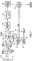
- FIG. 1 A block diagram of one embodiment of a document scanning and image processing method and apparatus, is shown in Fig. 1.
- the system enhances a scanned multi-bit grayscale image to sharpen image edges therein and then threshold the enhanced image into a single bit binary video signal.
- the document 10 is scanned one line at a time by a scanner and specifically by a 5000-by-1 cell charge coupled device (CCD) array 12 located therein.
- the array 12 is positioned in front of the document and is perpendicularly oriented to the direction of travel of the document shown by arrow 14.
- a light source (not shown) illuminates the document 10 and light reflected therefrom enters the optical system 16.
- Optical system 16 ensures that light is focused on the CCD array 12. In practice, optical system 16 is set to overscan each horizontal scanning line so the full image will be scanned even if document 10 was off center or tilted and/or if the CCD 10 becomes slightly horizontally mis-aligned with respect to the document.
- each cell of the CCD array 12 provides an analog output which is proportional to the intensity of the light that is reflected from a portion of scanned area 18 and which is focused onto that cell.
- Each of two CCD channels provides cells; one group for the odd pixels and the other for the even pixels.
- a stream of sequential pixels for both the even and odd channels are simultaneously shifted out of the array on leads 24 and 28 for the even and odd pixels, respectively, for each scanned line in scanned document 10.
- Each channel of pixel information is then converted by a respective analog-to-digital (A/D) converter.
- A/D analog-to-digital
- A/D converter 26 receives even channel pixel information over lead 24 emanating from CCD array 12 and under control of appropriate "convert" control pulses appearing on lead 32, provides eight-bit digital equivalent pixel values on leads 27.
- A/D converter 29 receives odd channel pixel information over lead 28 emanating from CCD array 12 and, under control of appropriate convert pulses appearing on lead 31, provides eight-bit digital equivalent pixel values on leads 30.
- the convert pulses are provided by pixel addressing circuit 34. This circuit also generates the (X,Y) address of the current pixel in the document that is being scanned. This address consists of vertical (Y) pixel address, YCNT (Y count), appearing on leads 35 and horizontal (X) pixel address, XCNT (X count), appearing on leads 36.
- System clock pulses are provided by clock circuit 38 and appear on lead 39.
- Pre-scan processing circuit 40 includes a multiplexer (not shown) that routes incoming pixels on an alternating basis from even channel leads 27 and odd channel leads 30 to a single stream of pixel information. All timing and control signals for the multiplexer are controlled by system clock signals appearing over lead 39. The multiplexer produces a single stream of pixels.
- the pre-scan processing circuit may also include a shading correction circuit and a gamma correction circuit.
- the shading correction circuit stores appropriate correction factors about illumination falloff and optical correction factors to insure uniform illumination of the image.
- a gamma correction circuit also stores information that is used to compensate for different transfer characteristics occurring among different types of film. These characteristics generally include intensity rolloff, film rise, distance, and the like. Use of such a circuit would be more appropriate when scanning microfilm instead of original documents.
- A/D converters 26, 29 digitize the image signal into 256 levels and the signal was passed through pre-scan processing circuit 40.
- the signal is next sent to a programmable DC offset circuit 42 where the 0-255 8-bit/pixel unsigned data is then converted to signed data by subtracting a programmably fixed DC offset equal to approximately one half of the expected peak to peak range of the input signal. This results in signal pixel values typically from -128 to 127. Signed numbers are necessary to allow the following DC attenuation section to reduce the low spatial frequency component towards zero while maintaining the original "polarity" of the data.
- the subtraction can be done by a discrete adder/subtracter or alternatively, may be done in conjunction with a Gamma Correction circuit (not shown) or a shading correction circuit (not shown) or in digital filter 48.
- the signed signal data is then "DC attenuated" using a finite impulse response (FIR) digital filter 46.
- FIR finite impulse response
- a finite impulse response (FIR) convolution filter requires that, the coefficients (tap weights) be selected to sum to between 0-1 where this sum defines the DC gain (1-DC attenuation).
- a second FIR convolution filter may be used for image enhancement and the coefficients of both filters can be combined to establish a new set of coefficients appropriate for the single filter.
- Figure 2 illustrates the one dimensional filter responses for the enhancement filter 44 and the 50% DC attenuation filter 46.
- the final response curve represents the combined filter response 48.
- the gain at zero frequency or DC is one.
- the gain increases to a gain of two units at a frequency of 100 line pairs per inch in the case of a 200 dot per inch scanner.
- the numbers under the title are the coefficients (tap weights) that will be used in the enhancement filter 44 to achieve the desired frequency response.
- the second graph illustrates the response characteristics of a DC attenuation filter 46 and its coefficients.
- the third graph illustrates the combined response 48 after combining the other two response curves 44 and 46.
- the response characteristics of the attenuation filter 46 is subtracted from the response curve of the enhancement filter 44 resulting in a combined filter response 48 that has the DC response of the attenuation filter 46 and the high frequency response of the enhancement filter 44.
- the attenuation filter 46 had a 70% (taps sum to .7) DC attenuation
- the DC response of the combined filter 48 would be 30%. Best results have been obtained using a DC attenuation of between 70%-80% with the combined response being 30%-20% respectively.
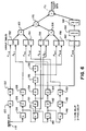
- Fig. 3 that illustrates a filter kernel 50 and how the coefficients of the one dimensional filter are located along the horizontal X axis as X-2, X-1, XY0, X+1, and X+2 from left to right.
- the coefficients of the same one dimensional filter are applied to the vertical Y axis as Y-2, Y-1, XY0, Y+1, and Y+2.
- the coefficients now form the basis for a two dimensional filter.
- the values in the open spaces or boxes of the four quadrants of the graph may be derived using orthogonal combinations of the two one dimensional filters or if desired, may be assigned appropriate constants. In Fig. 3, these constants have been set to zero.
- Fig. 3 illustrate how a two dimensional DC attenuation filter 52 is combined with the two dimensional enhancement filter 54 to create a combined convolution FIR filter 56.
- Filter 58 is comprised of one dimensional X filter section 5 pixels in length.
- the X filter section 58 has image pixels inputted thereto from a suitable source via bus 60, and includes a series of one-pixel delay buffers 62, 64, 66, and 68. Buffers 62, 64, 66, and 68 are connected in series by serial buffer buses 70, 72, and 74 respectively, with input bus 60 coupled to the input port of the first buffer 62. A buffer output bus 76 is coupled to the output port of buffer 68.
- the incoming video signal has been digitized prior to being processed by filter 58. It is understood that the number of bits required is a function of the resolution desired and is typically 6-8 bits.
- Image pixel input bus 60, serial buffer buses 70, 72, 74, and 76 are coupled through buses 80, 82, 84, 86, and 88 and multipliers 90, 92, 94, 96, and 98 to adder 100.
- Multipliers 90, 92, 94, 96, and 98 service to multiply the image pixels in buses 80, 82, 84, 86, and 88 by preset filter factors (as shown in filter grids in Fig. 3) [h (x-1)] [h (x-2)] [h (xy)], etc. input to multipliers 90, 92, 94, 96, and 98 through control buses 102.
- the processed image pixels outputted by multipliers 90, 92, 94, 96 and 98 are summed by adder 100, to provide composite one-dimensional (i.e. X) filtered image pixels.
- Fig. 5 illustrates how five one dimensional filters 104, 106, 108, 110, and 112 of the type shown in Fig. 4 can be used to make a two-dimensional convolution FIR filter.
- the stream of image pixels input bus 114 to the two dimensional filter 116 are clocked through the line delay buffers 118, 120, 122, and 124 (that correspond to pixel delay buffers 62, 64, 66, and 68 of Fig. 4).
- the coefficient multipliers that correspond to multipliers 90, 92, 94, 96 and 98 in Fig.
- Figure 5 shows how a plurality of one dimensional FIR convolution filters can be combined using line delays 118, 120, 122, and 124 to delay each of five scan lines to produce a 5-by-5 two dimensional FIR convolution filter.
- Convolution can substantially compensate for the loss in resolution.
- the amplitude of the pixel situated at the beginning of the edge will be substantially increased while that of all surrounding pixels will be decreased although by an amount less than the increase.
- the amplitude of the former pixel will reach a peak at a positive value that is substantially higher than the original intensity level, thereby producing a "spike” in the convolution output, while the values of the pixels will become somewhat negative creating a "moat” around the peaked value.
- the size of the window is set to 5-by-5 in order to achieve a good compromise between hardware costs and complexity and resulting image quality.
- 5X5 low pass convolution FIR filter which provides DC attenuation of the digital signal. This represents the preferred values for the filter if there were no cost constraints on the amount of memory being required for such a filter.
- the values of the coefficients are selected to sum to one.
- the convolution enhancement filter was combined with digital DC attenuation filter is intended to reduce the gain to less than one.
- the DC gain was attenuated by 70-80% so that the overall gain of the combined filters resulted in a 30-20% DC response.
- Fig. 6 illustrates a second embodiment of a circuit that can generate the convolution FIR filter coefficients and output filtered 8 bit data for the central pixel of the combined filter.
- filter kernel 50 A block diagram for an implementation of the filter kernel shown in the upper righthand corner of Fig. 3 and is labeled as filter kernel 50.
- Each pixel value Y-2, Y-1, x-2, x-1, XY0, etc. is applied to the matrix a row at a time as the pixel values are sent seriatim on the data line 118.
- Y-2 the only value used in the first row is delayed by two pixel delays 120, 122.
- Y-1 in the second row is delayed by line delay 124 and pixel delays 126, 128.
- the third row x-2, x-1, XY0, x+1, x+2 are all delayed by line delay 130 and as the pixel values move to the right in the row, each one must pass through one additional line delay than those on its immediate left.
- x-2 is delayed only by line delay 130
- x-1 is delayed by pixel delay 132 with XY0 being delayed by pixel delays 132, 134, with x+1 delayed by pixel delays 132, 134 and 136.
- x+2 is delayed by pixel delays 132, 134, 136, and 138.
- Y-2 and Y-1 are inputted to lookup table 152 where each pixel value is multiplied by the appropriate coefficient that is part of the filter matrix; the products are outputted to adder/latch 162 where the values of Y+1 and Y+2 and their respective products are summed with the output from lookup table 154.
- the product values associated with x-2 and x-1 are outputted from lookup table 156 to add/latch 164, which receives and combines the output of lookup table 158 with the output of lookup table 156.
- the product associated with central pixel h (XY0) is performed in lookup table 160 the output of which is sent to two latches 166, 168 to introduce the appropriate delay so that it will arrive at the final add/latch 172 at the appropriate time.
- the outputs of add/latches 162 and 164 are summed and latched by add/latch 170.
- the final add/latch 172 sums the output of add/latch 170 with the product value of the central pixel and its coefficient 170 resulting in the filtered 8 bit value for the central pixel of the matrix.
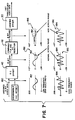
- the result is that the spatial distribution of the errors allows an observer to integrate the average percent reflectance in a small region and, therefore "see” a near continuum of gray level.
- “ordered dither” or pseudorandom thresholding is simply a form of electronic screening. Adding a known waveform to an image signal prior to comparison to a fixed threshold is equivalent to comparing the input signal with a variable threshold of the same shape as the waveform added.
- a unique feature of ordered dither is that it results in a dispersed set of black and white dots instead of a single "dot" as in the analog of the photomechanical screening process.
- Unsigned 8 bit video data enters on lead 180 coming from the A/D converters 26 and 29 and pre-scan processing circuit 40 which may be in the form of low frequency grayscale information 182 or high frequency text information 184 both in the range from 0-255.
- the DC attenuation of that filter has substantially reduced the peak-peak range of the low frequency signal.
- the screen or dither range 186 should be selected such that the low frequency signals tend to remain within the reduced screen range. Thus, it can be seen that when this low frequency signal is fed to the ordered dither circuit 20, it will act over the attenuated range so that the low frequency signal 182 will get the full effect of the dither.
- the high frequency signal 184 has a portion of the signal fall outside the new screen range 186; accordingly, when this signal is applied to the ordered dither circuit 20, the amplitudes remain unchanged and the peaks of the high frequency signal 184 goes outside of the range 186 of the dither and therefore, pass through unaffected.
- the present invention is useful in image management systems and generally in systems for enhancing and thresholding scanned multi-bit images.
- the present invention advantageously provides improved tonal rendition from the scanned image and sharpens edges occurring in the image.
Landscapes
- Engineering & Computer Science (AREA)
- Multimedia (AREA)
- Signal Processing (AREA)
- Physics & Mathematics (AREA)
- General Physics & Mathematics (AREA)
- Theoretical Computer Science (AREA)
- Facsimile Image Signal Circuits (AREA)
- Image Processing (AREA)
- Facsimile Scanning Arrangements (AREA)
Abstract
Claims (13)
- Appareil de traitement de signal d'image comportant un moyen (12) d'analyse d'image qui possède un moyen optique (16) permettant le balayage d'un original suivant deux dimensions, un moyen de conversion photoélectrique servant à convertir une image optique obtenue à l'aide du moyen optique (16) en un signal électrique, et un moyen de conversion numérique (26, 29) servant à convertir ledit signal électrique en un signal numérique, caractérisé par :
un moyen de décalage de niveau continu(42) servant à retirer un niveau continu prédéterminé audit signal numérique afin de produire un décalage de niveau continu prédéterminé, de sorte qu'on modifie l'intervalle dudit signal numérique pour produire des valeurs de signal numérique dotées d'un signe ;
un moyen filtre d'atténuation numérique(48) possédant un gain inférieur à l'unité et appliquant une atténuation de niveau continu audit signal numérique avec signe afin de ramener vers zéro les composantes de basse fréquence spatiale tout en maintenant la polarité des valeurs des pixels, de sorte qu'on améliore la netteté de l'image ; et
un moyen de conversion par agitation (20) qui utilise au moins une matrice d'agitation principale pour ajouter audit signal numérique atténué un signal formant une séquence de pseudo-bruit afin de produire une fixation de seuil pseudo-aléatoire pour ledit signal numérique. - Appareil de traitement de signal d'image selon la revendication 1, où ledit moyen de conversion par agitation est en outre caractérisé par plusieurs sous-matrices d'agitation.
- Appareil de traitement de signal d'image selon la revendication 2, où ledit moyen filtre d'atténuation numérique (48) comporte un premier filtre à convolution à réponse impulsionnelle finie (46).
- Appareil de traitement de signal d'image selon la revendication 2, où lesdites sous-matrices d'agitation sont disposées dans ladite matrice d'agitation principale de façon que les moyennes des niveaux d'agitation desdites sous-matrices d'agitation représentent une haute fréquence spatiale.
- Appareil de traitement de signal d'image selon la revendication 3, où ledit moyen filtre d'atténuation numérique comporte en outre un deuxième filtre à convolution à réponse impulsionnelle finie (44) servant à produire une amélioration de l'image.
- Appareil de traitement de signal d'image selon la revendication 5, où lesdits premier et deuxième filtres à convolution à réponse impulsionnelle finie (46, 44) sont combinés en un unique filtre (48).
- Procédé de traitement de signal d'image obtenu par analyse par balayage tramé, ligne par ligne, de documents originaux et conversion du signal analogique résultant en un signal numérique qui en est représentatif, caractérisé par les opérations suivantes :
modifier l'intervalle dudit signal numérique en appliquant un décalage de niveau continu prédéterminé (42) de manière à obtenir des valeurs de pixels dotées d'un signe ;
atténuer le niveau continu dudit signal numérique avec signe (48) afin de ramener vers zéro les composantes à basse fréquence spatiale tout en maintenant la polarité des valeurs des pixels, de sorte qu'on améliore la netteté de l'image ; et
ajouter audit signal numérique atténué un signal formant une séquence de pseudo-bruit afin de produire une fixation de seuil pseudo-aléatoire (20) pour ledit signal numérique atténué. - Procédé selon la revendication 7, où le décalage de niveau continu appliqué audit signal numérique est fixé à environ la moitié de l'intervalle total dudit signal numérique.
- Procédé selon la revendication 8, où ledit signal formant une séquence de pseudo-bruit est ajouté sous la forme d'une agitation ordonnée.
- Procédé selon la revendication 9, où ledit procédé de traitement de signaux d'image est en outre caractérisé par l'opération consistant à améliorer la représentation dudit signal numérique.
- Procédé selon la revendication 10, où on combine ladite opération d'atténuation de niveau continu dudit signal numérique et ladite opération d'amélioration.
- Procédé selon la revendication 9, où on ajuste les niveaux de seuil de l'agitation ordonnée de façon qu'ils soient compatibles avec le signal atténué en niveau continu.
- Procédé selon la revendication 12, où l'agitation ordonnée produit une fréquence spatiale élevée de façon à faciliter l'effet d'intégration par l'oeil humain.
Applications Claiming Priority (5)
| Application Number | Priority Date | Filing Date | Title |
|---|---|---|---|
| US301679 | 1981-09-14 | ||
| US301677 | 1981-09-14 | ||
| US07/301,677 US4912569A (en) | 1989-01-24 | 1989-01-24 | Method for thresholding an image signal |
| US07/301,679 US4918543A (en) | 1989-01-24 | 1989-01-24 | Apparatus for thresholding an image signal |
| PCT/US1990/000371 WO1990009005A1 (fr) | 1989-01-24 | 1990-01-23 | Procede et appareil etablissant le seuil d'un signal d'image |
Publications (2)
| Publication Number | Publication Date |
|---|---|
| EP0429560A1 EP0429560A1 (fr) | 1991-06-05 |
| EP0429560B1 true EP0429560B1 (fr) | 1995-11-08 |
Family
ID=26972536
Family Applications (1)
| Application Number | Title | Priority Date | Filing Date |
|---|---|---|---|
| EP90903279A Expired - Lifetime EP0429560B1 (fr) | 1989-01-24 | 1990-01-23 | Procede et appareil etablissant le seuil d'un signal d'image |
Country Status (4)
| Country | Link |
|---|---|
| EP (1) | EP0429560B1 (fr) |
| JP (1) | JPH03503591A (fr) |
| DE (1) | DE69023458T2 (fr) |
| WO (1) | WO1990009005A1 (fr) |
Families Citing this family (1)
| Publication number | Priority date | Publication date | Assignee | Title |
|---|---|---|---|---|
| JP2870451B2 (ja) * | 1995-05-25 | 1999-03-17 | 日本電気株式会社 | 画像処理装置 |
Family Cites Families (2)
| Publication number | Priority date | Publication date | Assignee | Title |
|---|---|---|---|---|
| US4723298A (en) * | 1985-03-27 | 1988-02-02 | Fingermatrix, Inc. | Image compression technique |
| US4720871A (en) * | 1986-06-13 | 1988-01-19 | Hughes Aircraft Company | Digital image convolution processor method and apparatus |
-
1990
- 1990-01-23 EP EP90903279A patent/EP0429560B1/fr not_active Expired - Lifetime
- 1990-01-23 DE DE69023458T patent/DE69023458T2/de not_active Expired - Lifetime
- 1990-01-23 WO PCT/US1990/000371 patent/WO1990009005A1/fr not_active Ceased
- 1990-01-23 JP JP2503407A patent/JPH03503591A/ja active Pending
Also Published As
| Publication number | Publication date |
|---|---|
| DE69023458D1 (de) | 1995-12-14 |
| WO1990009005A1 (fr) | 1990-08-09 |
| JPH03503591A (ja) | 1991-08-08 |
| DE69023458T2 (de) | 1996-07-11 |
| EP0429560A1 (fr) | 1991-06-05 |
Similar Documents
| Publication | Publication Date | Title |
|---|---|---|
| US4912569A (en) | Method for thresholding an image signal | |
| Stoffel et al. | A survey of electronic techniques for pictorial image reproduction | |
| EP0497304B1 (fr) | Appareil de traitement d'images | |
| US6101285A (en) | Filter for producing continuous tone images from halftone digital images data | |
| EP0562813B1 (fr) | Système et procédé pour transformer les images à demi-teinte en images à teinte continue | |
| Miceli et al. | Inverse halftoning | |
| EP0402162B1 (fr) | Traitement d'image avec opérateurs d'amélioration du bruit pour la réduction de moiré et/ou la génération des pointes aléatoires | |
| US5343283A (en) | Scan/print system for performing image processing and an image selection unit for use in the scan/print system | |
| EP0393619A2 (fr) | Appareil pour traitement d'images | |
| US4918543A (en) | Apparatus for thresholding an image signal | |
| EP0781034A2 (fr) | Appareil et procédé de traitement d'images | |
| CN1066137A (zh) | 图象处理装置 | |
| JPH0481382B2 (fr) | ||
| JPH0787313A (ja) | 画像処理方式および画像処理装置 | |
| EP0429560B1 (fr) | Procede et appareil etablissant le seuil d'un signal d'image | |
| EP0382581B1 (fr) | Appareil de traitement d'images | |
| US6134355A (en) | Binarization using a local average, and using error diffusion | |
| EP0814600A2 (fr) | Procédé et système pour le traitement de données d'images | |
| JP3165225B2 (ja) | 画像処理装置および画像処理方法 | |
| EP0304218A2 (fr) | Procédé et appareil pour la mise en oeuvre d'une opération de demi-teinte | |
| Zeggel et al. | Halftoning with error diffusion on an image-adaptive raster | |
| JP2938545B2 (ja) | 画像信号処理装置 | |
| Williams et al. | Halftone processing in the Xerox 7650 image scanner | |
| KR920008327B1 (ko) | 화상신호 전처리장치 | |
| JPH05176168A (ja) | 適応中間調処理方式 |
Legal Events
| Date | Code | Title | Description |
|---|---|---|---|
| PUAI | Public reference made under article 153(3) epc to a published international application that has entered the european phase |
Free format text: ORIGINAL CODE: 0009012 |
|
| 17P | Request for examination filed |
Effective date: 19901217 |
|
| AK | Designated contracting states |
Kind code of ref document: A1 Designated state(s): BE DE GB |
|
| 17Q | First examination report despatched |
Effective date: 19940530 |
|
| GRAA | (expected) grant |
Free format text: ORIGINAL CODE: 0009210 |
|
| AK | Designated contracting states |
Kind code of ref document: B1 Designated state(s): BE DE GB |
|
| REF | Corresponds to: |
Ref document number: 69023458 Country of ref document: DE Date of ref document: 19951214 |
|
| PLBE | No opposition filed within time limit |
Free format text: ORIGINAL CODE: 0009261 |
|
| STAA | Information on the status of an ep patent application or granted ep patent |
Free format text: STATUS: NO OPPOSITION FILED WITHIN TIME LIMIT |
|
| 26N | No opposition filed | ||
| REG | Reference to a national code |
Ref country code: GB Ref legal event code: IF02 |
|
| PGFP | Annual fee paid to national office [announced via postgrant information from national office to epo] |
Ref country code: BE Payment date: 20020220 Year of fee payment: 13 |
|
| PG25 | Lapsed in a contracting state [announced via postgrant information from national office to epo] |
Ref country code: BE Free format text: LAPSE BECAUSE OF NON-PAYMENT OF DUE FEES Effective date: 20030131 |
|
| PGFP | Annual fee paid to national office [announced via postgrant information from national office to epo] |
Ref country code: DE Payment date: 20090130 Year of fee payment: 20 |
|
| PGFP | Annual fee paid to national office [announced via postgrant information from national office to epo] |
Ref country code: GB Payment date: 20081211 Year of fee payment: 20 |
|
| REG | Reference to a national code |
Ref country code: GB Ref legal event code: PE20 Expiry date: 20100122 |
|
| PG25 | Lapsed in a contracting state [announced via postgrant information from national office to epo] |
Ref country code: GB Free format text: LAPSE BECAUSE OF EXPIRATION OF PROTECTION Effective date: 20100122 |
|
| PG25 | Lapsed in a contracting state [announced via postgrant information from national office to epo] |
Ref country code: DE Free format text: LAPSE BECAUSE OF EXPIRATION OF PROTECTION Effective date: 20100123 |