EP0429695B1 - Steuergerät, insbesondere zur Steuerung von Funktionen eines Kraftfahrzeugs - Google Patents
Steuergerät, insbesondere zur Steuerung von Funktionen eines Kraftfahrzeugs Download PDFInfo
- Publication number
- EP0429695B1 EP0429695B1 EP89121923A EP89121923A EP0429695B1 EP 0429695 B1 EP0429695 B1 EP 0429695B1 EP 89121923 A EP89121923 A EP 89121923A EP 89121923 A EP89121923 A EP 89121923A EP 0429695 B1 EP0429695 B1 EP 0429695B1
- Authority
- EP
- European Patent Office
- Prior art keywords
- analog
- digital
- ground
- plate
- plate part
- Prior art date
- Legal status (The legal status is an assumption and is not a legal conclusion. Google has not performed a legal analysis and makes no representation as to the accuracy of the status listed.)
- Expired - Lifetime
Links
- 230000002093 peripheral effect Effects 0.000 claims description 2
- 238000007781 pre-processing Methods 0.000 claims 1
- 230000005855 radiation Effects 0.000 description 3
- 239000003990 capacitor Substances 0.000 description 2
- 230000008878 coupling Effects 0.000 description 2
- 238000010168 coupling process Methods 0.000 description 2
- 238000005859 coupling reaction Methods 0.000 description 2
- 239000000853 adhesive Substances 0.000 description 1
- 230000001070 adhesive effect Effects 0.000 description 1
- 239000000919 ceramic Substances 0.000 description 1
- 238000005516 engineering process Methods 0.000 description 1
- 230000035515 penetration Effects 0.000 description 1
- 239000000758 substrate Substances 0.000 description 1
Images
Classifications
-
- B—PERFORMING OPERATIONS; TRANSPORTING
- B60—VEHICLES IN GENERAL
- B60R—VEHICLES, VEHICLE FITTINGS, OR VEHICLE PARTS, NOT OTHERWISE PROVIDED FOR
- B60R16/00—Electric or fluid circuits specially adapted for vehicles and not otherwise provided for; Arrangement of elements of electric or fluid circuits specially adapted for vehicles and not otherwise provided for
- B60R16/02—Electric or fluid circuits specially adapted for vehicles and not otherwise provided for; Arrangement of elements of electric or fluid circuits specially adapted for vehicles and not otherwise provided for electric constitutive elements
- B60R16/023—Electric or fluid circuits specially adapted for vehicles and not otherwise provided for; Arrangement of elements of electric or fluid circuits specially adapted for vehicles and not otherwise provided for electric constitutive elements for transmission of signals between vehicle parts or subsystems
-
- H—ELECTRICITY
- H05—ELECTRIC TECHNIQUES NOT OTHERWISE PROVIDED FOR
- H05K—PRINTED CIRCUITS; CASINGS OR CONSTRUCTIONAL DETAILS OF ELECTRIC APPARATUS; MANUFACTURE OF ASSEMBLAGES OF ELECTRICAL COMPONENTS
- H05K1/00—Printed circuits
- H05K1/02—Details
- H05K1/0213—Electrical arrangements not otherwise provided for
- H05K1/0216—Reduction of cross-talk, noise or electromagnetic interference
-
- H—ELECTRICITY
- H05—ELECTRIC TECHNIQUES NOT OTHERWISE PROVIDED FOR
- H05K—PRINTED CIRCUITS; CASINGS OR CONSTRUCTIONAL DETAILS OF ELECTRIC APPARATUS; MANUFACTURE OF ASSEMBLAGES OF ELECTRICAL COMPONENTS
- H05K9/00—Screening of apparatus or components against electric or magnetic fields
- H05K9/0007—Casings
- H05K9/002—Casings with localised screening
- H05K9/0039—Galvanic coupling of ground layer on printed circuit board [PCB] to conductive casing
-
- H—ELECTRICITY
- H05—ELECTRIC TECHNIQUES NOT OTHERWISE PROVIDED FOR
- H05K—PRINTED CIRCUITS; CASINGS OR CONSTRUCTIONAL DETAILS OF ELECTRIC APPARATUS; MANUFACTURE OF ASSEMBLAGES OF ELECTRICAL COMPONENTS
- H05K1/00—Printed circuits
- H05K1/02—Details
- H05K1/0213—Electrical arrangements not otherwise provided for
- H05K1/0215—Grounding of printed circuits by connection to external grounding means
-
- H—ELECTRICITY
- H05—ELECTRIC TECHNIQUES NOT OTHERWISE PROVIDED FOR
- H05K—PRINTED CIRCUITS; CASINGS OR CONSTRUCTIONAL DETAILS OF ELECTRIC APPARATUS; MANUFACTURE OF ASSEMBLAGES OF ELECTRICAL COMPONENTS
- H05K1/00—Printed circuits
- H05K1/02—Details
- H05K1/0213—Electrical arrangements not otherwise provided for
- H05K1/0216—Reduction of cross-talk, noise or electromagnetic interference
- H05K1/023—Reduction of cross-talk, noise or electromagnetic interference using auxiliary mounted passive components or auxiliary substances
- H05K1/0231—Capacitors or dielectric substances
-
- H—ELECTRICITY
- H05—ELECTRIC TECHNIQUES NOT OTHERWISE PROVIDED FOR
- H05K—PRINTED CIRCUITS; CASINGS OR CONSTRUCTIONAL DETAILS OF ELECTRIC APPARATUS; MANUFACTURE OF ASSEMBLAGES OF ELECTRICAL COMPONENTS
- H05K1/00—Printed circuits
- H05K1/02—Details
- H05K1/03—Use of materials for the substrate
- H05K1/0306—Inorganic insulating substrates, e.g. ceramic, glass
-
- H—ELECTRICITY
- H05—ELECTRIC TECHNIQUES NOT OTHERWISE PROVIDED FOR
- H05K—PRINTED CIRCUITS; CASINGS OR CONSTRUCTIONAL DETAILS OF ELECTRIC APPARATUS; MANUFACTURE OF ASSEMBLAGES OF ELECTRICAL COMPONENTS
- H05K2201/00—Indexing scheme relating to printed circuits covered by H05K1/00
- H05K2201/07—Electric details
- H05K2201/0707—Shielding
- H05K2201/0715—Shielding provided by an outer layer of PCB
-
- H—ELECTRICITY
- H05—ELECTRIC TECHNIQUES NOT OTHERWISE PROVIDED FOR
- H05K—PRINTED CIRCUITS; CASINGS OR CONSTRUCTIONAL DETAILS OF ELECTRIC APPARATUS; MANUFACTURE OF ASSEMBLAGES OF ELECTRICAL COMPONENTS
- H05K2201/00—Indexing scheme relating to printed circuits covered by H05K1/00
- H05K2201/09—Shape and layout
- H05K2201/09209—Shape and layout details of conductors
- H05K2201/0929—Conductive planes
- H05K2201/093—Layout of power planes, ground planes or power supply conductors, e.g. having special clearance holes therein
-
- H—ELECTRICITY
- H05—ELECTRIC TECHNIQUES NOT OTHERWISE PROVIDED FOR
- H05K—PRINTED CIRCUITS; CASINGS OR CONSTRUCTIONAL DETAILS OF ELECTRIC APPARATUS; MANUFACTURE OF ASSEMBLAGES OF ELECTRICAL COMPONENTS
- H05K2201/00—Indexing scheme relating to printed circuits covered by H05K1/00
- H05K2201/09—Shape and layout
- H05K2201/09209—Shape and layout details of conductors
- H05K2201/09654—Shape and layout details of conductors covering at least two types of conductors provided for in H05K2201/09218 - H05K2201/095
- H05K2201/09663—Divided layout, i.e. conductors divided in two or more parts
-
- H—ELECTRICITY
- H05—ELECTRIC TECHNIQUES NOT OTHERWISE PROVIDED FOR
- H05K—PRINTED CIRCUITS; CASINGS OR CONSTRUCTIONAL DETAILS OF ELECTRIC APPARATUS; MANUFACTURE OF ASSEMBLAGES OF ELECTRICAL COMPONENTS
- H05K2201/00—Indexing scheme relating to printed circuits covered by H05K1/00
- H05K2201/09—Shape and layout
- H05K2201/09818—Shape or layout details not covered by a single group of H05K2201/09009 - H05K2201/09809
- H05K2201/09972—Partitioned, e.g. portions of a PCB dedicated to different functions; Boundary lines therefore; Portions of a PCB being processed separately or differently
Definitions
- the invention relates to a control device as described in German utility model 87 15 073.
- Such a control device has an analog part with analog components and a digital part with digital components, which are arranged on a support plate which has "printed" connecting lines for the components on the top, connecting contacts for connecting signal lines and ground connection points.
- the invention is characterized in claim 1. It consists essentially in the proposal to provide at least two plate parts with electrically isolated areal masses, an analog mass and a digital mass, and on the plate part with the digital mass all "fast" digital components of the control unit, e.g. B. processor and memory, to be arranged, which are characterized by the processing of signals with steep signal edges ( ⁇ 1 ⁇ sec per edge) and / or with a high clock frequency (> 500 kHz).
- a separate analog ground is assigned to the analog part with signal line and its shielding. The analog ground and the digital ground are then spatially separated from one another with the electrically conductive base plate of the control unit, to which the ground line coming from the outside is also connected.
- the invention is based on the finding that, in the known technology, a high-frequency potential difference between the base plate on the one hand and the areal mass and the parts electrically connected to it - ground connection line, signal screen - is formed, which is emitted via these lines.
- the pulse currents in the digital part e.g. between a microprocessor and a memory (EPROM): These impulse currents have very high-frequency components, which already produce disturbing voltage drops in short ground leads and in the base plate - due to the low penetration depth.
- the plate part with the digital mass can form a separate support plate which carries the digital components on its upper side.
- the two plate parts form a one-piece supporting plate, on the underside of which the analog mass and the digital mass are arranged electrically separated from one another.
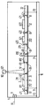
- An embodiment of this type is described in more detail with reference to the figure, which shows a cross section through a control unit 1 - z.
- a one-piece support plate 2 for example a ceramic substrate, is divided into two sub-areas, namely a plate part 21 and one Plate part 22, the upper sides with 211 and 221 and the lower sides with 212 and 222 respectively.
- the plate part 21 On the top side 211 of the plate part 21 there are predominantly analog input modules 811, 812 of the analog part (no "fast” digital modules), a printed circuit (not shown) for connecting the input modules to one another and with a connection contact 51 and with ground connection points 410 to 413. All ground connection points are connected via connectors 61 - through holes in the plate part 21 - to the analog ground 31 on the underside 212 of the plate part 21.
- a signal line 92 - e.g. B. coming from a rotary sensor - is connected to the connection contact 51 and its screen 921 to the ground connection point 412.
- the ground connection point 410 enables, for example, a short ground connection of the module 812.
- the plate part 22 has on its underside 222 an areal mass - digital mass 32.
- all "fast" digital components 821, 822 of the control unit - e.g. B. a microprocessor and at least one peripheral digital module, for. B. an EMPROM - arranged and interconnected by not shown printed circuits - address and data bus.
- connectors 61 in holes in the plate part 22 are used to connect the digital ground 32 to the ground connection points 420 to 422 on the upper side 221.
- the ground connection point 420 enables a short connection of the component 821 or a point of a printed circuit to the digital ground 32.
- the analog ground 31 is connected at least at one point via a ground connection point 411 and a connecting line 71 - bonding wire - and the digital ground 32 via a ground connection point 421 and a connecting line 72 with different points of the electrically conductive base plate 10. From this a connecting line 73 leads to one Ground terminal 11 for connecting a ground line 91.
- the height of the residual interference voltage effective between base plate 10 - ground line 91 - and analog ground 31 - shield 921 - depends on the number of connections between base plate 10 and analog ground 31. Particularly good results can be achieved if this analog mass is subdivided into a plurality of surface areas, each of which is connected to the closest connection point of the base plate 10 via an associated ground connection point and a connecting line.
- the digital part can also be distributed on two partial plates with assigned digital masses; a plate part can form a one-piece support plate with the plate part assigned to the analog part, which has two mutually insulated ground surfaces on the underside - analog and digital ground.
- the support plate or plate parts are preferably attached to the base plate 10 by adhesive.
Landscapes
- Engineering & Computer Science (AREA)
- Microelectronics & Electronic Packaging (AREA)
- Mechanical Engineering (AREA)
- Physics & Mathematics (AREA)
- Electromagnetism (AREA)
- Shielding Devices Or Components To Electric Or Magnetic Fields (AREA)
- Combined Controls Of Internal Combustion Engines (AREA)
- Logic Circuits (AREA)
- Electrical Control Of Ignition Timing (AREA)
Description
- Die Erfindung geht aus von einem Steuergerät wie es in dem deutschen Gebrauchsmuster 87 15 073 beschrieben ist.
- Ein solches Steuergerät hat einen Analogteil mit analogen Bausteinen und einen Digitalteil mit Digitalbausteinen, die auf einer Tragplatte angeordnet sind, die auf der Oberseite "gedruckte" Verbindungsleitungen für die Bausteine, Anschlußkontakte zum Anschluß von Signalleitungen und Masseanschlußpunkte aufweist. Auf der Unterseite der Tragplatte ist eine flächenhafte Masseschicht angeordnet, mit der die Masseanschlußpunkte auf der Oberseite auf kürzestem Weg verbunden sind; hierzu dienen Verbindern, die durch Löcher in der Tragplatte hindurchgehen, wodurch sich sehr niederohmige Masseverbindungen ergeben.
- Trotz dieses vorteilhaften Aufbaus wurde bei solchen Steuergeräten eine Hochfrequenzabstrahlung gemessen, die in manchen Fällen stört. Dies ist vor allem dann der Fall, wenn aus dem Steuergerät führende Leitungen, insbesondere die Masseleitung, mit weiteren Leitungen, die zu anderen elektronischen Geräten führen, einen Kabelbaum bilden: Hierbei entsteht eine sehr enge Kopplung zwischen mehreren Geräten, die zur gegenseitigen Störung führen kann. Der Erfindung liegt die Aufgabe zugrunde, ein Steuergerät so aufzubauen, daß die Störstrahlung weiter reduziert wird.
- Die Erfindung ist in Patentanspruch 1 gekennzeichnet. Sie besteht im wesentlichen in dem Vorschlag, wenigstens zwei Plattenteile mit elektrisch voneinander isolierten flächenhaften Massen, einer Analogmasse und einer Digitalmasse, vorzusehen und auf dem Plattenteil mit der Digitalmasse alle "schnellen" Digitalbauteile des Steuergerätes, z. B. Prozessor und Speicher, anzuordnen, die durch die Verarbeitung von Signalen mit steilen Signalflanken (<1 µsec pro Flanke) und/oder mit hoher Taktfrequenz (> 500 kHz) gekennzeichnet sind. Dem Analogteil mit Signalleitung und ihrer Abschirmung ist eine davon getrennte Analogmasse zugeordnet. Die Analogmasse und die Digitalmasse sind dann räumlich getrennt voneinander mit der elektrisch leitenden Grundplatte des Steuergeräts verbunden, andie auch die von außen kommende Masseleitung angeschlossen wird.
- Die Erfindung beruht auf der Feststellung, daß sich bei der bekannten Technik ein hochfrequenter Potentialunterschied zwischen der Grundplatte einerseits und der flächenhaften Masse und den damit elektrisch verbundenen Teilen - Masseanschlußleitung, Signalschirm - ausbildet, der über diese Leitungen abgestrahlt wird. Als Ursache für diese Störspannung wurden die Impulsströme im Digitalteil, z.B. zwischen einem Mikroprozessor und einem Speicher (EPROM), ermittelt: Diese Impulsströme haben sehr hochfrequente Anteile, die bereits in kurzen Masseanschlußleitungen und in der Grundplatte - wegen der geringen Eindringtiefe - störende Spannungsabfälle erzeugen. Durch die erfindungsgemäße Abtrennung einer separaten Digitalmasse von der Analogmasse des Analogteils läßt sich die Störabstrahlung drastisch reduzieren, da zwischen den beiden Massen praktisch keine hochfrequente Kopplung mehr besteht.
- Im Rahmen der Erfindung kann das Plattenteil mit der Digitalmasse eine gesonderte Tragplatte zu bilden, die auf ihrer Oberseite die Digitalbausteine trägt. Meist ist es jedoch vorteilhafter, wenn die beiden Plattenteile eine einstückige Tragplatte bilden, auf deren Unterseite nebeneinander die Analogmasse und die Digitalmasse elektrisch voneinander getrennt angeordnet sind. Ein Ausführungsbeispiel dieser Art wird anhand der Figur näher beschrieben, die einen Querschnitt durch ein Steuergerät 1 - z. B. ein Zündsteuergerät - mit einer elektrisch leitenden Grundplatte 10 in schematisierter Form zeigt. Eine einstückige Tragplatte 2, z.B. ein Keramiksubstrat, ist in zwei Teilbereiche gegliedert, nämlich ein Plattenteil 21 und ein Plattenteil 22, deren Oberseiten mit 211 bzw. 221 und deren Unterseiten mit 212 bzw. 222 bezeichnet sind.
- Auf der Oberseite 211 des Plattenteils 21 sind überwiegend analoge Eingangsbausteine 811, 812 des Analogteils (keine "schnellen" Digitalbausteine), eine gedruckte Schaltung, (nicht dargestellt) zur Verbindung der Eingangsbausteine untereinander und mit einem Anschlußkontakt 51 und mit Masseanschlußpunkten 410 bis 413 angeordnet. Alle Masseanschlußpunkte sind über Verbinder 61 - durch Löcher in dem Plattenteil 21 geführt - mit der Analogmasse 31 auf der Unserseite 212 des Plattenteils 21 verbunden.
- Eine Signalleitung 92 - z. B. von einem Drehsensor kommend - ist mit dem Anschlußkontakt 51 und ihr Schirm 921 mit dem Masseanschlußpunkt 412 verbunden. Der Masseanschlußpunkt 410 ermöglicht beispielsweise einen kurzen Masseanschluß des Bausteins 812.
- Das Plattenteil 22 hat auf seiner Unterseite 222 eine flächenhafte Masse - Digitalmasse 32. Auf der Oberseite 221 sind alle "schnellen" Digitalbausteine 821, 822 des Steuergerätes - z. B. ein Mikroprozessor und mindestens ein peripherer Digitalbaustein, z. B. ein EMPROM - angeordnet und durch nicht dargestellte gedruckte Schaltungen - Adreß- und Datenbus - miteinander verbunden. Zur Verbindung der Digitalmasse 32 mit Masseanschlußpunkten 420 bis 422 auf der Oberseite 221 dienen auch hier Verbinder 61 in Löchern des Plattenteils 22. Der Masseanschlußpunkt 420 ermöglicht eine kurze Verbindung des Bausteins 821 oder eines Punktes einer gedruckten Schaltung mit der Digitalmasse 32.
- Die Analogmasse 31 ist an wenigstens einer Stelle über einen Masseanschlußpunkt 411 und eine Verbindungsleitung 71 - Bonddraht - und die Digitalmasse 32 über einen Masseanschlußpunkt 421 und eine Verbindungsleitung 72 gleichstromleitend mit unterschiedlichen Punkten der elektrisch leitenden Grundplatte 10 verbunden. Von dieser führt eine Verbindungsleitung 73 zu einer Masseklemme 11 zum Anschluß einer Masseleitung 91. Die Höhe der zwischen Grundplatte 10 - Masseleitung 91 - und Analogmasse 31 - Schirm 921 - wirksamen Reststörspannung ist von der Anzahl der Verbindungen zwischen Grundplatte 10 und Analogmasse 31 abhängig. Besonders gute Ergebnisse sind zu erzielen, wenn diese Analogmasse in mehrere Flächenbereiche unterteilt ist, von denen jeder über einen zugehörigen Masseanschlußpunkt und eine Verbindungsleitung an den nächstliegenden Anschlußpunkt der Grundplatte 10 angeschlossen ist. Dabei ist es meist zweckmäßig, nur eine Verbindung gleichstromleitend und die anderen kapazitiv auszubilden. So ist z. B. in der Figur zwischen dem Masseanschlußpunkt 413 und der Verbindungsleitung 71 ein Kondensator 810 mit 22 µF eingelötet. Solche Kondesatoren verhindern dabei Störungen durch eine räumliche Verteilung von Gleichströmen einer Leistungsstufe - z. B. der Zündendstufe - auf dem Eingangsteil.
- Abweichend vom beschriebenen Ausführungsbeispiel kann der Digitalteil auch auf zwei Teilplatten mit zugeordneten Digitalmassen verteilt sein; ein Plattenteil kann dabei mit dem dem Analogteil zugeordneten Plattenteil eine einstückige Tragplatte bilden, die auf der Unterseite zwei von einander isolierte Masseflächen - Analog- und Digitalmasse - hat.
- Die Tragplatte oder Plattenteile sind vorzugsweise mit der Grundplatte 10 durch Klebstoff befestigt.
Claims (3)
- Steuergerät (1) insbesondere zur Steuerung von Funktionen eines Kraftfahrzeugs,- mit einem Analogteil zur Aufbereitung eines Eingangssignals,-- mit einem ersten Plattenteil (21) mit Oberseite (211) und Unterseite (212), das--- auf der Unterseite (212) eine flächenhafte Teilmasse - Analogmasse (31) - und das--- auf der Oberseite (211) analoge Eingangsbausteine (811, 812), gedruckte Verbindungsleitungen, einen Anschlußkontakt (51) für eine Signalleitung (92), Masseanschlußpunkte (410 bis 413), die mit der Anlogmasse (31) durch Löcher in dem Plattenteil (21) auf kürzestem Wege verbunden sind, insbesondere zum Anschluß eines Schirmes (921) der Signalleitung (92), aufweist;- mit einem Digitalteil zur Gewinnung eines Steuersignals aus dem Eingangssignal,-- mit mindestens einem Plattenteil (22) mit Oberseite (221) und Unterseite (222), das--- auf seiner Unterseite (222) eine flächenhafte Masseschicht - Digitalmasse (32) - hat und das--- auf seiner Oberseite (221) Digitalbausteine (821, 822) mit einem Mikroprozessor und mindestens einem peripheren Digitalbaustein sowie gedruckte Verbindungsleitungen, die einen Daten- und Adreßbus einschließen, und Massenanschlußpunkte (420 bis 422), die durch Löcher in dem Plattenteil (22) auf kürzestem Wege mit der Digitalmasse (32) verbunden sind, aufweist;- mit einer elektrische leitenden Grundplatte (10), die die Plattenteile (21, 22) trägt, und mit der mindestens ein Masseanschlußpunkt (411) des Analogteils und räumlich davon getrennt ein Masseanschlußpunkt (421) des Digitalteils sowie eine Masseklemme (11) zum Anschluß einer Masseleitung (91) verbunden sind.
- Steuergerät nach Anspruch 1,
dadurch gekennzeichnet,
daß die Plattenteile (21, 22) von Analogteil und Digitalteil eine einstückige Tragplatte (2) mit voneinander getrennter flächenhafter Analog und Digitalmasse (31, 32) bilden. - Steuergerät nach Anspruch 1,
dadurch gekennzeichnet,
daß das Plattenteil (21) des Analogteils mehrere räumlich voneinander entfernte Masseanschlußpunkte hat, die auf kürzestem Wege mit der Tragplatte (10) verbunden sind, wobei mindestens eine dieser Verbindungen gleichstromleitend und mindestens eine weitere Verbindung kapazitiv ausgebildet ist.
Priority Applications (4)
| Application Number | Priority Date | Filing Date | Title |
|---|---|---|---|
| DE8989121923T DE58902722D1 (de) | 1989-11-28 | 1989-11-28 | Steuergeraet, insbesondere zur steuerung von funktionen eines kraftfahrzeugs. |
| EP89121923A EP0429695B1 (de) | 1989-11-28 | 1989-11-28 | Steuergerät, insbesondere zur Steuerung von Funktionen eines Kraftfahrzeugs |
| US07/618,644 US5231308A (en) | 1989-11-28 | 1990-11-27 | Control device for controlling functions in a motor vehicle |
| JP2323364A JPH03189370A (ja) | 1989-11-28 | 1990-11-28 | 制御装置 |
Applications Claiming Priority (1)
| Application Number | Priority Date | Filing Date | Title |
|---|---|---|---|
| EP89121923A EP0429695B1 (de) | 1989-11-28 | 1989-11-28 | Steuergerät, insbesondere zur Steuerung von Funktionen eines Kraftfahrzeugs |
Publications (2)
| Publication Number | Publication Date |
|---|---|
| EP0429695A1 EP0429695A1 (de) | 1991-06-05 |
| EP0429695B1 true EP0429695B1 (de) | 1992-11-11 |
Family
ID=8202169
Family Applications (1)
| Application Number | Title | Priority Date | Filing Date |
|---|---|---|---|
| EP89121923A Expired - Lifetime EP0429695B1 (de) | 1989-11-28 | 1989-11-28 | Steuergerät, insbesondere zur Steuerung von Funktionen eines Kraftfahrzeugs |
Country Status (4)
| Country | Link |
|---|---|
| US (1) | US5231308A (de) |
| EP (1) | EP0429695B1 (de) |
| JP (1) | JPH03189370A (de) |
| DE (1) | DE58902722D1 (de) |
Families Citing this family (14)
| Publication number | Priority date | Publication date | Assignee | Title |
|---|---|---|---|---|
| US5561584A (en) * | 1993-09-30 | 1996-10-01 | Vimak Corporation | Electrical ground plane apparatus |
| US5640293A (en) * | 1993-11-10 | 1997-06-17 | Ice Corporation | High-current, high-voltage solid state switch |
| JPH07235775A (ja) * | 1994-02-21 | 1995-09-05 | Mitsubishi Electric Corp | 多層プリント配線基板 |
| DE19516918A1 (de) * | 1995-05-09 | 1996-11-14 | Bosch Gmbh Robert | Steuergerät, insbesondere zur Steuerung von Funktionen eines Kraftfahrzeugs |
| DE19536848A1 (de) * | 1995-10-02 | 1997-04-03 | Bosch Gmbh Robert | Baugruppenträger für ein elektronisches Steuergerät mit signalverarbeitenden Bauelementen und schnell arbeitenden digitalen Bauelementen |
| JPH09326586A (ja) * | 1996-06-05 | 1997-12-16 | Alps Electric Co Ltd | 高周波電子機器 |
| US6088215A (en) * | 1997-11-03 | 2000-07-11 | Motorola, Inc. | Capacitor and method of manufacture |
| US20070002599A1 (en) * | 2003-02-28 | 2007-01-04 | Robin Caven | Circuit board and arrangement for minimizing thermal and electromagnetic effects |
| DE10309520A1 (de) * | 2003-03-05 | 2004-09-16 | Robert Bosch Gmbh | Trägervorrichtung für elektrische Bauelemente |
| US9179235B2 (en) | 2008-11-07 | 2015-11-03 | Adobe Systems Incorporated | Meta-parameter control for digital audio data |
| GB2486855B (en) * | 2009-09-17 | 2014-07-23 | Hewlett Packard Development Co | Apparatus and method for reproducing an audio signal |
| TR201000142A2 (tr) * | 2010-01-08 | 2011-07-21 | Vestel Elektroni̇k San. Ve Ti̇c. A.Ş. | Toprak anahtarlama bileşeni. |
| JPWO2011086612A1 (ja) * | 2010-01-15 | 2013-05-16 | パナソニック株式会社 | 半導体装置 |
| JP5786483B2 (ja) * | 2011-06-20 | 2015-09-30 | ソニー株式会社 | 通信装置 |
Family Cites Families (7)
| Publication number | Priority date | Publication date | Assignee | Title |
|---|---|---|---|---|
| DE2409660A1 (de) * | 1974-02-28 | 1975-09-25 | Siemens Ag | Elektrische schalt-, steuer- und/oder regeleinrichtung fuer elektrische geraete in einem fahrzeug |
| US4218578A (en) * | 1978-08-04 | 1980-08-19 | Burr-Brown Research Corp. | RF Shield for an electronic component |
| JPS57130842A (en) * | 1981-02-06 | 1982-08-13 | Nippon Denso Co Ltd | Electronic system for mounting on vehicle |
| US5019945A (en) * | 1983-05-31 | 1991-05-28 | Trw Inc. | Backplane interconnection system |
| DE8715073U1 (de) * | 1987-11-12 | 1988-02-25 | Siemens AG, 1000 Berlin und 8000 München | Elektronische Baueinheit zur Steuerung von Funktionen eines Kraftfahrzeugs |
| DE3837206C2 (de) * | 1988-11-02 | 1998-07-23 | Bosch Gmbh Robert | Elektrisches Schaltgerät |
| US5053926A (en) * | 1989-11-16 | 1991-10-01 | Voice Data Image Corporation Inc. | Electronic equipment cabinet cover panel with integrated connector assembly |
-
1989
- 1989-11-28 EP EP89121923A patent/EP0429695B1/de not_active Expired - Lifetime
- 1989-11-28 DE DE8989121923T patent/DE58902722D1/de not_active Expired - Lifetime
-
1990
- 1990-11-27 US US07/618,644 patent/US5231308A/en not_active Expired - Fee Related
- 1990-11-28 JP JP2323364A patent/JPH03189370A/ja active Pending
Also Published As
| Publication number | Publication date |
|---|---|
| DE58902722D1 (de) | 1992-12-17 |
| JPH03189370A (ja) | 1991-08-19 |
| EP0429695A1 (de) | 1991-06-05 |
| US5231308A (en) | 1993-07-27 |
Similar Documents
| Publication | Publication Date | Title |
|---|---|---|
| EP0429695B1 (de) | Steuergerät, insbesondere zur Steuerung von Funktionen eines Kraftfahrzeugs | |
| EP0712267B1 (de) | Modulare Steuerungsanlage mit integriertem Feldbusanschluss | |
| DE3809503A1 (de) | Koaxialkondensator fuer einen impulsgenerator | |
| DE3411550A1 (de) | Oberschalige elektrische waage | |
| EP0801884B1 (de) | Baugruppenträger für ein elektronisches steuergerät mit signalverarbeitenden bauelementen und schnell arbeitenden digitalen bauelementen | |
| DE8715073U1 (de) | Elektronische Baueinheit zur Steuerung von Funktionen eines Kraftfahrzeugs | |
| EP0027544B1 (de) | Oberflächenwellen-Bauteil | |
| DE8916194U1 (de) | Steuergerät, insbesondere zur Steuerung von Funktionen eines Kraftfahrzeugs | |
| DE2709397C2 (de) | Elektrischer Lageänderungsschalter | |
| DE1936899A1 (de) | Baugruppentraeger fuer Steuer- bzw. Regelanlagen | |
| DE2309869A1 (de) | Schaltung in dickfilm-technik | |
| DE3904461C1 (en) | Multipole radio-frequency plug connection | |
| DE2165143C3 (de) | Elektrodenanordnung für einen stabförmigen, piezoelektrischen Biegungsschwinger | |
| DE3730899C1 (en) | Input device for electrical switching | |
| AT401444B (de) | Überspannungsschutzeinrichtung für daten verarbeitende geräte | |
| EP0607843A1 (de) | Einstückiges Isolierteil, insbesondere Spritzgiessteil | |
| DE102015213631A1 (de) | Schaltungsplatine | |
| EP0061990A1 (de) | Überspannungsableiter mit eine Säule von Ableiterelementen umschliessenden Abschirmkörpern | |
| EP0802598A2 (de) | Fronttafelmodul | |
| DE6928695U (de) | Baugruppentraeger fuer steuer- bzw. regelanlagen | |
| DE19738736A1 (de) | Kontaktsensor | |
| EP1455557B1 (de) | Trägervorrichtung für elektrische Bauelemente | |
| DE4309173C2 (de) | Spannungsversorgung von Abschlußwiderständen | |
| DE19834381C2 (de) | Leiterplatte | |
| DE1766307C3 (de) | Kapazitiv durchstimmbares UHF-Bandfilter |
Legal Events
| Date | Code | Title | Description |
|---|---|---|---|
| PUAI | Public reference made under article 153(3) epc to a published international application that has entered the european phase |
Free format text: ORIGINAL CODE: 0009012 |
|
| 17P | Request for examination filed |
Effective date: 19901220 |
|
| AK | Designated contracting states |
Kind code of ref document: A1 Designated state(s): AT BE CH DE ES FR GB GR IT LI LU NL SE |
|
| RBV | Designated contracting states (corrected) |
Designated state(s): DE FR GB IT |
|
| 17Q | First examination report despatched |
Effective date: 19920424 |
|
| GRAA | (expected) grant |
Free format text: ORIGINAL CODE: 0009210 |
|
| AK | Designated contracting states |
Kind code of ref document: B1 Designated state(s): DE FR GB IT |
|
| REF | Corresponds to: |
Ref document number: 58902722 Country of ref document: DE Date of ref document: 19921217 |
|
| ET | Fr: translation filed | ||
| ITF | It: translation for a ep patent filed | ||
| GBT | Gb: translation of ep patent filed (gb section 77(6)(a)/1977) |
Effective date: 19930115 |
|
| PLBI | Opposition filed |
Free format text: ORIGINAL CODE: 0009260 |
|
| 26 | Opposition filed |
Opponent name: ROBERT BOSCH GMBH Effective date: 19930811 |
|
| PGFP | Annual fee paid to national office [announced via postgrant information from national office to epo] |
Ref country code: FR Payment date: 19931125 Year of fee payment: 5 |
|
| PGFP | Annual fee paid to national office [announced via postgrant information from national office to epo] |
Ref country code: DE Payment date: 19940119 Year of fee payment: 5 |
|
| RDAG | Patent revoked |
Free format text: ORIGINAL CODE: 0009271 |
|
| STAA | Information on the status of an ep patent application or granted ep patent |
Free format text: STATUS: PATENT REVOKED |
|
| PGFP | Annual fee paid to national office [announced via postgrant information from national office to epo] |
Ref country code: GB Payment date: 19941018 Year of fee payment: 6 |
|
| 27W | Patent revoked |
Effective date: 19940622 |
|
| GBPR | Gb: patent revoked under art. 102 of the ep convention designating the uk as contracting state |
Free format text: 940622 |