EP0430040A2 - Verfahren zur Herstellung einer Durchgangsleitung oder einer Verbindungsleitung durch ein duktiles Metall in einer integrierten Schaltung unter Verwendung von mechanischem Festreiben - Google Patents
Verfahren zur Herstellung einer Durchgangsleitung oder einer Verbindungsleitung durch ein duktiles Metall in einer integrierten Schaltung unter Verwendung von mechanischem Festreiben Download PDFInfo
- Publication number
- EP0430040A2 EP0430040A2 EP90122197A EP90122197A EP0430040A2 EP 0430040 A2 EP0430040 A2 EP 0430040A2 EP 90122197 A EP90122197 A EP 90122197A EP 90122197 A EP90122197 A EP 90122197A EP 0430040 A2 EP0430040 A2 EP 0430040A2
- Authority
- EP
- European Patent Office
- Prior art keywords
- metal
- dielectric layer
- layer
- interconnect line
- order
- Prior art date
- Legal status (The legal status is an assumption and is not a legal conclusion. Google has not performed a legal analysis and makes no representation as to the accuracy of the status listed.)
- Withdrawn
Links
Images





Classifications
-
- H—ELECTRICITY
- H10—SEMICONDUCTOR DEVICES; ELECTRIC SOLID-STATE DEVICES NOT OTHERWISE PROVIDED FOR
- H10W—GENERIC PACKAGES, INTERCONNECTIONS, CONNECTORS OR OTHER CONSTRUCTIONAL DETAILS OF DEVICES COVERED BY CLASS H10
- H10W20/00—Interconnections in chips, wafers or substrates
- H10W20/01—Manufacture or treatment
- H10W20/071—Manufacture or treatment of dielectric parts thereof
- H10W20/081—Manufacture or treatment of dielectric parts thereof by forming openings in the dielectric parts
- H10W20/084—Manufacture or treatment of dielectric parts thereof by forming openings in the dielectric parts for dual-damascene structures
-
- H—ELECTRICITY
- H10—SEMICONDUCTOR DEVICES; ELECTRIC SOLID-STATE DEVICES NOT OTHERWISE PROVIDED FOR
- H10P—GENERIC PROCESSES OR APPARATUS FOR THE MANUFACTURE OR TREATMENT OF DEVICES COVERED BY CLASS H10
- H10P52/00—Grinding, lapping or polishing of wafers, substrates or parts of devices
- H10P52/40—Chemomechanical polishing [CMP]
- H10P52/403—Chemomechanical polishing [CMP] of conductive or resistive materials
-
- H—ELECTRICITY
- H10—SEMICONDUCTOR DEVICES; ELECTRIC SOLID-STATE DEVICES NOT OTHERWISE PROVIDED FOR
- H10W—GENERIC PACKAGES, INTERCONNECTIONS, CONNECTORS OR OTHER CONSTRUCTIONAL DETAILS OF DEVICES COVERED BY CLASS H10
- H10W20/00—Interconnections in chips, wafers or substrates
- H10W20/01—Manufacture or treatment
- H10W20/031—Manufacture or treatment of conductive parts of the interconnections
- H10W20/056—Manufacture or treatment of conductive parts of the interconnections by filling conductive material into holes, grooves or trenches
- H10W20/059—Manufacture or treatment of conductive parts of the interconnections by filling conductive material into holes, grooves or trenches by reflowing or applying pressure
-
- H—ELECTRICITY
- H10—SEMICONDUCTOR DEVICES; ELECTRIC SOLID-STATE DEVICES NOT OTHERWISE PROVIDED FOR
- H10W—GENERIC PACKAGES, INTERCONNECTIONS, CONNECTORS OR OTHER CONSTRUCTIONAL DETAILS OF DEVICES COVERED BY CLASS H10
- H10W20/00—Interconnections in chips, wafers or substrates
- H10W20/01—Manufacture or treatment
- H10W20/031—Manufacture or treatment of conductive parts of the interconnections
- H10W20/062—Manufacture or treatment of conductive parts of the interconnections by smoothing of conductive parts, e.g. by planarisation
-
- H—ELECTRICITY
- H10—SEMICONDUCTOR DEVICES; ELECTRIC SOLID-STATE DEVICES NOT OTHERWISE PROVIDED FOR
- H10W—GENERIC PACKAGES, INTERCONNECTIONS, CONNECTORS OR OTHER CONSTRUCTIONAL DETAILS OF DEVICES COVERED BY CLASS H10
- H10W20/00—Interconnections in chips, wafers or substrates
- H10W20/01—Manufacture or treatment
- H10W20/071—Manufacture or treatment of dielectric parts thereof
- H10W20/081—Manufacture or treatment of dielectric parts thereof by forming openings in the dielectric parts
Definitions
- This invention relates to semiconductor manufacturing technology and, more specifically, to methods for creating metal interconnections between conductive layers and metal interconnect lines in sub-micron manufacturing processes.
- metal interconnect lines are affected by particle contamination and defective metal layer etches. Generally, particle contamination is responsible for open circuits in the metal interconnect system, while a defective etch of a metal layer may result in both shorted or open circuits.
- particle contamination is responsible for open circuits in the metal interconnect system, while a defective etch of a metal layer may result in both shorted or open circuits.
- Another problem associated with the creation of metal interconnect lines is that metal layers are relatively difficult to etch as compared, for example, to silicon dioxide.
- electromigration becomes a more significant problem. Since electromigration in semiconductor devices is generally associated the use of pure aluminum for interconnect lines, the problem is most easily eliminated by alloying other metals, such as copper, with aluminum.
- alloys of aluminum that do not exhibit at least minimal grain-boundary diffusion in the presence of an electric current are generally relatively difficult to etch using plasma or reactive-ion etching techniques.
- the present invention dramatically improves the step coverage of a ductile metal used as an interconnect material within an integrated circuit by utilizing mechanical energy to force the ductile metal into channels and vias.
- the process begins with a wafer having a dielectric layer, the upper surface of which has been planarized. Following a first masking step, channels are etched in the upper surface of the dielectric layer. Following a second masking step, vias are etched through the dielectric layer to the conductive layer below where contact is to be made. A layer of ductile metal is then deposited on top of the dielectric layer by any one of a number of means (e.g., sputter deposition or chemical vapor deposition).
- the ductile metal layer is then mechanically deformed so that it is worked into the vias and interconnect channels. Mechanical deformation is accomplished by maintaining a rotating disk or vibrating pad in contact with the metal layer. Disks and pads made of metal or polymeric compounds have been used successfully. The wafer is then slurry polished until all excess metal has been removed and the topography is coplanar with the planar surface of the dielectric layer. Metal remains only in the vias and interconnect channels. This method of creating via plugs and interconnect channels has several important advantages over the prior art. Firstly, via walls may be etched more steeply since mechanical energy is used to force metal into them. Secondly, no etching of metal layers is necessary for the creation of either interconnect lines or via plugs.
- vias and channels are etched in the planarized dielectric layer, and these channels are filled with metal using the aforementioned process.
- the fact that no etching is required permits the use of nearly any ductile metal or alloy thereof, without regard for the ease with which it is etched.
- Figure 1 is an isometric view of a portion of a partially-processed semiconductor wafer which depicts a field-effect transistor (FET) having as a drain a conductively-doped region within a silicon substrate, all of which is overlaid by a planarized dielectric layer of silicon dioxide;
- FET field-effect transistor
- Figure 2 is an isometric view of the wafer portion of Figure 1, following a first photomasking step which defines an interconnect channel and a first dry oxide etch which creates the channel;
- Figure 3 is an isometric view of the wafer portion of Figure 2, following removal of the first photo mask
- Figure 4 is an isometric view of the wafer portion of Figure 3, following a second photomasking step which defines an interconnect via superimposed on the previously created channel and a second dry oxide etch which creates the via;
- Figure 5 is an isometric view of the wafer portion of Figure 4, following removal of the second photo mask
- Figure 6 is an isometric view of the wafer portion of Figure 5, with the frontal portion up to the plane defined by broken line 6-6 removed to show a cross-section through the via;
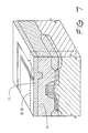
- Figure 7 is an isometric view of the wafer portion of Figure 5, following the chemical vapor deposition of a ductile metal layer on top thereof;
- Figure 8 is an isometric view of the wafer portion of Figure 7, with the frontal portion up to the plane defined by broken line 8-8 removed to show a cross-section through the via;
- Figure 9 is an isometric view of the wafer portion of Figure 7, following the mechanical smearing or deformation of the metal layer;
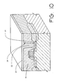
- Figure 10 is an isometric view of the wafer portion of Figure 9, with the frontal portion up to the plane defined by broken line 8-8 removed to show a cross-section through the via;
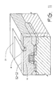
- Figure 11 is an isometric view of the wafer portion of Figure 9, following a slurry polish that removes all excess metal;
- Figure 12 is an isometric view of the wafer portion of Figure 11, with the frontal portion up to the plane defined by broken line 12-12 removed to show a cross-section through the via.
- a portion of a partially-processed semiconductor wafer 11 is shown in Figure 1.
- a field-effect transistor (FET) 12 has been constructed on top of a silicon substrate 13, a portion of which has been doped to serve as the FET drain 14, and another portion of which has been doped to serve as the FET source 15. All topography has been covered by a silicon dioxide dielectric layer 16 the upper surface of which has been planarized. In order to completely describe the present invention, it will be assumed that an interconnect line must be formed on top of dielectric layer 16 and that the interconnect line must connect with FET drain 14.
- a first photoresist mask 17 has been applied to wafer 11 on top of dielectric layer 15.
- First photo mask 17 defines the geometries of desired interconnect lines on the surface of dielectric layer 15. Only a single interconnect line will be created on the wafer portion shown in this Figure.
- a first dry oxide etch forms interconnect line channel 18 which will be filled with ductile metal in a later step, thus becoming one of the desired interconnect lines on the wafer.
- channel 18 etched in dielectric layer 15 is shown following the removal of first photo mask 17.
- a second photoresist mask 19 which defines interconnect vias, has been applied to wafer 11.
- a single via will be formed on the wafer portion depicted in this Figure.
- the via will be positioned such that it, at least partially, coincides with the already etched channel 18 so that when the via plug and interconnect line are formed, they will be in electrical communication with one another.
- a second dry oxide etch forms via 20 which, along with channel 18, will be filled with ductile metal in a later step.
- channel 18 and via 20 are shown following the removal of second photo mask 19.
- FIG. 6 is a cross-sectional view through the plane defined by broken lines 6-6 of Figure 5, the internal geometry of via 20 is more readily apparent. FET drain 14 is exposed by via 20.
- a conformal ductile metal layer 21 has been deposited on top of dielectric layer 15.
- Deposition may be done by any number of means such as chemical vapor deposition or sputter deposition.
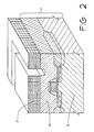
- FIG 8 is a cross-sectional view through the plane defined by broken lines 8-8 of Figure 7, step coverage of the via plug 22 within the via is poor.
- via plug 22 doesn't contact FET drain 14.
- the transistor would be inoperative if no further steps were taken to improve the quality of this connection.
- ductile metal layer 21 has been deformed by smearing using a rotating disk or a vibrating pad held in contact therewith.
- the disk or pad may be made of any material having sufficient structural integrity to transfer mechanical energy to metal layer 21.
- the metal of layer 21 is forced into channel 18 and via 20 (not shown in this Figure).
- Disks made of metal and durable polymer plastics such as tetrafluoroethylene have been used successfully.
- Rotation of a disk may be unidirectional or reciprocatingly bidirectional, with bidirectional being the preferred mode. Bidirectional smearing tends to compact the metal within the via or channel more uniformly. If a vibrating pad is used for the smearing operation, it may be vibrated in either a omni-directional or orbital mode.
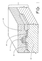
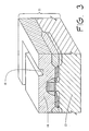
- Figure 10 is a cross-sectional view through the plane defined by broken lines 10-10 of Figure 9, step coverage of the via plug 22 within via 20 has been greatly improved, with sound plug-to-FET-drain contact having been obtained.
- a slurry polish has been used to remove all excess metal from metal layer 21 from the planarized surface of dielectric layer 15, such that ductile metal remains only in channel 18 and via 20 (not shown in this Figure). At this point via plug 22 (not shown in this Figure) and interconnect line 23 are fully formed.
- An optional high-temperature step may be used to recrystallize the metal which forms via plug 22 and interconnect line 23.
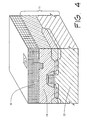
- Figure 12 is a cross-sectional view through the plane defined by broken lines 12-12 of Figure 11, the final appearance of the cross-section of via plug 22 is shown.
- both via plugs and interconnect lines are conductive paths, the difference being that via plugs provide vertical conductive paths, while interconnect lines provide horizontal conductive paths.
- a depression (whether via or channel) is etched into a dielectric layer, ductile metal is deposited on top of the dielectric layer, the ductile metal is then mechanically deformed by smearing using a disk or pad, such as those heretofore described, so that metal is forced into the depression.
- a slurry polishing operation removes the excess metal, leaving metal only in the depression.
Landscapes
- Internal Circuitry In Semiconductor Integrated Circuit Devices (AREA)
Applications Claiming Priority (2)
| Application Number | Priority Date | Filing Date | Title |
|---|---|---|---|
| US44161189A | 1989-11-27 | 1989-11-27 | |
| US441611 | 1989-11-27 |
Publications (2)
| Publication Number | Publication Date |
|---|---|
| EP0430040A2 true EP0430040A2 (de) | 1991-06-05 |
| EP0430040A3 EP0430040A3 (en) | 1992-05-20 |
Family
ID=23753577
Family Applications (1)
| Application Number | Title | Priority Date | Filing Date |
|---|---|---|---|
| EP19900122197 Withdrawn EP0430040A3 (en) | 1989-11-27 | 1990-11-20 | Method of forming a conductive via plug or an interconnect line of ductile metal within an integrated circuit using mechanical smearing |
Country Status (2)
| Country | Link |
|---|---|
| EP (1) | EP0430040A3 (de) |
| JP (1) | JPH03220726A (de) |
Cited By (7)
| Publication number | Priority date | Publication date | Assignee | Title |
|---|---|---|---|---|
| EP0537749A1 (de) * | 1991-10-16 | 1993-04-21 | Nec Corporation | Verfahren zur Herstellung von elektrischen Verbindungen und Halbleiterbauelementen |
| WO1994000873A1 (de) * | 1992-06-30 | 1994-01-06 | Siemens Aktiengesellschaft | Herstellungsverfahren fur eine halbleiterspeicheranordnung |
| WO1994013008A3 (en) * | 1992-11-19 | 1994-07-21 | Electrotech Ltd | Forming a layer |
| WO1996002939A1 (en) * | 1994-07-13 | 1996-02-01 | Electrotech Limited | Method of introducing material in holes |
| EP0665580A3 (de) * | 1994-01-28 | 1997-03-05 | Texas Instruments Inc | Verfahren und Vorrichtung zur globalen Planarisierung der Oberfläche eines Halbleiter-Wafers. |
| US5714779A (en) * | 1992-06-30 | 1998-02-03 | Siemens Aktiengesellschaft | Semiconductor memory device having a transistor, a bit line, a word line and a stacked capacitor |
| EP0869550A2 (de) * | 1997-03-31 | 1998-10-07 | Siemens Aktiengesellschaft | Verbessertes Ätzen von kontaktlöchern |
Family Cites Families (1)
| Publication number | Priority date | Publication date | Assignee | Title |
|---|---|---|---|---|
| DE3788485T2 (de) * | 1986-09-30 | 1994-06-09 | Philips Nv | Verfahren zur Herstellung einer Planarleiterbahn durch isotropes Abscheiden von leitendem Werkstoff. |
-
1990
- 1990-11-20 EP EP19900122197 patent/EP0430040A3/en not_active Withdrawn
- 1990-11-22 JP JP2320607A patent/JPH03220726A/ja active Pending
Cited By (7)
| Publication number | Priority date | Publication date | Assignee | Title |
|---|---|---|---|---|
| EP0537749A1 (de) * | 1991-10-16 | 1993-04-21 | Nec Corporation | Verfahren zur Herstellung von elektrischen Verbindungen und Halbleiterbauelementen |
| WO1994000873A1 (de) * | 1992-06-30 | 1994-01-06 | Siemens Aktiengesellschaft | Herstellungsverfahren fur eine halbleiterspeicheranordnung |
| US5714779A (en) * | 1992-06-30 | 1998-02-03 | Siemens Aktiengesellschaft | Semiconductor memory device having a transistor, a bit line, a word line and a stacked capacitor |
| WO1994013008A3 (en) * | 1992-11-19 | 1994-07-21 | Electrotech Ltd | Forming a layer |
| EP0665580A3 (de) * | 1994-01-28 | 1997-03-05 | Texas Instruments Inc | Verfahren und Vorrichtung zur globalen Planarisierung der Oberfläche eines Halbleiter-Wafers. |
| WO1996002939A1 (en) * | 1994-07-13 | 1996-02-01 | Electrotech Limited | Method of introducing material in holes |
| EP0869550A2 (de) * | 1997-03-31 | 1998-10-07 | Siemens Aktiengesellschaft | Verbessertes Ätzen von kontaktlöchern |
Also Published As
| Publication number | Publication date |
|---|---|
| JPH03220726A (ja) | 1991-09-27 |
| EP0430040A3 (en) | 1992-05-20 |
Similar Documents
| Publication | Publication Date | Title |
|---|---|---|
| US6291137B1 (en) | Sidewall formation for sidewall patterning of sub 100 nm structures | |
| US4735679A (en) | Method of improving silicon-on-insulator uniformity | |
| JP4881895B2 (ja) | 半導体集積回路装置の製造方法 | |
| US6171951B1 (en) | Dual damascene method comprising ion implanting to densify dielectric layer and forming a hard mask layer with a tapered opening | |
| US4461672A (en) | Process for etching tapered vias in silicon dioxide | |
| US6221754B1 (en) | Method of fabricating a plug | |
| JPS61107748A (ja) | 半導体チツプの結線形成方法 | |
| JPH11168105A (ja) | 半導体集積回路の製造方法 | |
| US5437763A (en) | Method for formation of contact vias in integrated circuits | |
| US4631806A (en) | Method of producing integrated circuit structures | |
| US5073518A (en) | Process to mechanically and plastically deform solid ductile metal to fill contacts of conductive channels with ductile metal and process for dry polishing excess metal from a semiconductor wafer | |
| US5591673A (en) | Tungsten stud process for stacked via applications | |
| KR20040060112A (ko) | 반도체 소자 제조시 듀얼 다마신 공정을 이용한 콘텍형성방법 | |
| CA2465162A1 (en) | Silicon on insulator device with improved heat removal and method of manufacture | |
| US6114235A (en) | Multipurpose cap layer dielectric | |
| US6103455A (en) | Method to form a recess free deep contact | |
| US6277705B1 (en) | Method for fabricating an air-gap with a hard mask | |
| US6458710B1 (en) | Process for forming uniform multiple contact holes | |
| US5597983A (en) | Process of removing polymers in semiconductor vias | |
| US5412868A (en) | Process of removing polymers in semiconductor vias | |
| US6133133A (en) | Method for making an electrical contact to a node location and process for forming a conductive line or other circuit component | |
| US5510294A (en) | Method of forming vias for multilevel metallization | |
| JPH03220726A (ja) | 集積回路の露出平坦誘電層内に延性金属から成る導電路を形成させる方法 | |
| US6214737B1 (en) | Simplified sidewall formation for sidewall patterning of sub 100 nm structures | |
| JP2002299437A (ja) | 半導体装置の製造方法 |
Legal Events
| Date | Code | Title | Description |
|---|---|---|---|
| PUAI | Public reference made under article 153(3) epc to a published international application that has entered the european phase |
Free format text: ORIGINAL CODE: 0009012 |
|
| AK | Designated contracting states |
Kind code of ref document: A2 Designated state(s): DE |
|
| PUAL | Search report despatched |
Free format text: ORIGINAL CODE: 0009013 |
|
| AK | Designated contracting states |
Kind code of ref document: A3 Designated state(s): DE |
|
| 17P | Request for examination filed |
Effective date: 19920714 |
|
| STAA | Information on the status of an ep patent application or granted ep patent |
Free format text: STATUS: THE APPLICATION IS DEEMED TO BE WITHDRAWN |
|
| 18D | Application deemed to be withdrawn |
Effective date: 19940601 |