EP0430274A2 - Verfahren zur Herstellung von einem bipolaren Transistor - Google Patents
Verfahren zur Herstellung von einem bipolaren Transistor Download PDFInfo
- Publication number
- EP0430274A2 EP0430274A2 EP90122947A EP90122947A EP0430274A2 EP 0430274 A2 EP0430274 A2 EP 0430274A2 EP 90122947 A EP90122947 A EP 90122947A EP 90122947 A EP90122947 A EP 90122947A EP 0430274 A2 EP0430274 A2 EP 0430274A2
- Authority
- EP
- European Patent Office
- Prior art keywords
- impurity
- semiconductor film
- film layer
- layer
- region
- Prior art date
- Legal status (The legal status is an assumption and is not a legal conclusion. Google has not performed a legal analysis and makes no representation as to the accuracy of the status listed.)
- Withdrawn
Links
Images


Classifications
-
- H—ELECTRICITY
- H10—SEMICONDUCTOR DEVICES; ELECTRIC SOLID-STATE DEVICES NOT OTHERWISE PROVIDED FOR
- H10D—INORGANIC ELECTRIC SEMICONDUCTOR DEVICES
- H10D10/00—Bipolar junction transistors [BJT]
- H10D10/01—Manufacture or treatment
- H10D10/051—Manufacture or treatment of vertical BJTs
- H10D10/054—Forming extrinsic base regions on silicon substrate after insulating device isolation in vertical BJTs having single crystalline emitter, collector or base regions
-
- H—ELECTRICITY
- H10—SEMICONDUCTOR DEVICES; ELECTRIC SOLID-STATE DEVICES NOT OTHERWISE PROVIDED FOR
- H10P—GENERIC PROCESSES OR APPARATUS FOR THE MANUFACTURE OR TREATMENT OF DEVICES COVERED BY CLASS H10
- H10P32/00—Diffusion of dopants within, into or out of wafers, substrates or parts of devices
- H10P32/10—Diffusion of dopants within, into or out of semiconductor bodies or layers
- H10P32/14—Diffusion of dopants within, into or out of semiconductor bodies or layers within a single semiconductor body or layer in a solid phase; between different semiconductor bodies or layers, both in a solid phase
- H10P32/1408—Diffusion of dopants within, into or out of semiconductor bodies or layers within a single semiconductor body or layer in a solid phase; between different semiconductor bodies or layers, both in a solid phase from or through or into an external applied layer, e.g. photoresist or nitride layers
-
- H—ELECTRICITY
- H10—SEMICONDUCTOR DEVICES; ELECTRIC SOLID-STATE DEVICES NOT OTHERWISE PROVIDED FOR
- H10P—GENERIC PROCESSES OR APPARATUS FOR THE MANUFACTURE OR TREATMENT OF DEVICES COVERED BY CLASS H10
- H10P32/00—Diffusion of dopants within, into or out of wafers, substrates or parts of devices
- H10P32/10—Diffusion of dopants within, into or out of semiconductor bodies or layers
- H10P32/17—Diffusion of dopants within, into or out of semiconductor bodies or layers characterised by the semiconductor material
- H10P32/171—Diffusion of dopants within, into or out of semiconductor bodies or layers characterised by the semiconductor material being group IV material
-
- Y—GENERAL TAGGING OF NEW TECHNOLOGICAL DEVELOPMENTS; GENERAL TAGGING OF CROSS-SECTIONAL TECHNOLOGIES SPANNING OVER SEVERAL SECTIONS OF THE IPC; TECHNICAL SUBJECTS COVERED BY FORMER USPC CROSS-REFERENCE ART COLLECTIONS [XRACs] AND DIGESTS
- Y10—TECHNICAL SUBJECTS COVERED BY FORMER USPC
- Y10S—TECHNICAL SUBJECTS COVERED BY FORMER USPC CROSS-REFERENCE ART COLLECTIONS [XRACs] AND DIGESTS
- Y10S148/00—Metal treatment
- Y10S148/017—Clean surfaces
-
- Y—GENERAL TAGGING OF NEW TECHNOLOGICAL DEVELOPMENTS; GENERAL TAGGING OF CROSS-SECTIONAL TECHNOLOGIES SPANNING OVER SEVERAL SECTIONS OF THE IPC; TECHNICAL SUBJECTS COVERED BY FORMER USPC CROSS-REFERENCE ART COLLECTIONS [XRACs] AND DIGESTS
- Y10—TECHNICAL SUBJECTS COVERED BY FORMER USPC
- Y10S—TECHNICAL SUBJECTS COVERED BY FORMER USPC CROSS-REFERENCE ART COLLECTIONS [XRACs] AND DIGESTS
- Y10S148/00—Metal treatment
- Y10S148/034—Diffusion of boron or silicon
-
- Y—GENERAL TAGGING OF NEW TECHNOLOGICAL DEVELOPMENTS; GENERAL TAGGING OF CROSS-SECTIONAL TECHNOLOGIES SPANNING OVER SEVERAL SECTIONS OF THE IPC; TECHNICAL SUBJECTS COVERED BY FORMER USPC CROSS-REFERENCE ART COLLECTIONS [XRACs] AND DIGESTS
- Y10—TECHNICAL SUBJECTS COVERED BY FORMER USPC
- Y10S—TECHNICAL SUBJECTS COVERED BY FORMER USPC CROSS-REFERENCE ART COLLECTIONS [XRACs] AND DIGESTS
- Y10S148/00—Metal treatment
- Y10S148/144—Shallow diffusion
Definitions
- the present invention relates to the method of producing a bipolar transistor, and more specifically relates to the diffusing method of base region and emitter region.
- the base region is formed by depositing a semiconductor film layer on the preceding collector region at a predetermined thickness, and then by introducing an impurity into the semiconductor film layer at a predetermined concentration.
- the introduction of the impurity can be effected by ion implantation or the conventional diffusion technology.
- the size of bipolar transistor has been significantly reduced.
- the thickness of base region is reduced smaller and smaller in order to increase operating speed of the bipolar transistor.
- an emitter region is formed by depositing a semiconductor film layer on the preceding base region and then by introducing an impurity into the semiconductor film layer. Otherwise, the emitter region is formed by introducing one conductivity type of impurity into a semiconductor film layer disposed on the collector region after introducing another conductivity type of the impurity into the same semiconductor film layer to form precedingly the base region.
- the introduction of impurity is conventionally effected by the ion implantation into the semiconductor film layer. The ion implantation is carried out by firstly ionizing impurity atoms, then mass-filtering the ions, and thereafter accelerating the ions by a given energy to implant the ions into the semiconductor.
- the ion implantation features that an impurity introduction amount can be controlled accurately, and an impurity can be easily doped through an insulating film into the semiconductor. For this reason, the ion implantation is commonly utilized for the conventional impurity doping in the bipolar transistor process.
- the first object of the invention is to provide new doping method effective to introduce an impurity into a thin semiconductor film layer accurately and controllably to form a base region of the bipolar transistor.
- the second object of the invention is to provide new doping method effective to introduce an impurity into an emitter region of the bipolar transistor without affecting the impurity diffusion distribution of a precedingly formed base region.
- the bipolar transistor is produced by sequential steps of depositing a semiconductor film layer on a preceding formed collector region, cleaning the semiconductor film layer to expose an active surface, applying a gas containing an impurity component to the active surface while heating the substrate to form an impurity adsorption layer, and diffusing the impurity into the semiconductor film layer to form a base region.
- the adsorption step is carried out by applying a diborane gas containing a boron impurity to a silicon semiconductor film layer.
- the diffusion step is effected such that the semiconductor film layer is doped with P type impurity of boron so that the doped semiconductor film layer is used as a base region of the NPN bipolar transistor.
- the impurity gas is applied to the active surface of the semiconductor film layer to form an impurity adsorption layer.
- the amount of adsorbed impurity can be suitably controlled by adjusting the pressure of impurity gas and the application time interval thereof.
- Solid-phase diffusion of the impurity is effected from a diffusion source in the form of the impurity adsorption layer into the semiconductor film layer to form the base region.
- the impurity concentration and diffusion depth of the base region are controlled quite accurately by suitably setting the amount of the adsorbed impurity and the diffusion condition such as substrate temperature and heating time.
- the bipolar transistor is produced by sequential steps of depositing a semiconductor film layer on a previously formed base region, cleaning a surface of the semiconductor film layer to expose an active surface, applying a gas containing an impurity component to the active surface while heating the substrate to form an impurity adsorption layer, and diffusing the impurity into the semiconductor film layer to form an emitter region.
- the adsorption step is carried out by applying a diborane gas containing a boron impurity component to a silicon semiconductor film layer to form a boron adsorption layer. Consequently, there is formed an emitter region diffused by the P type impurity of boron to produce the PNP bipolar transistor.
- the impurity gas is applied to the semiconductor film layer deposited on the base region while heating the substrate so as to form the impurity adsorption layer on the active surface. Then, the solid-phase diffusion is effected from a diffusion source composed of the impurity adsorption layer into the semiconductor film layer to thereby from an emitter region. This impurity diffusion is confined within the semiconductor film layer which constitutes the emitter region, hence the impurity density distribution is not affected in the base region disposed under the emitter region.
- Figs. 1A - 1F are a process step diagram of an NPN bipolar transistor
- Fig. 2 is a block diagram of a production apparatus for use in the bipolar transistor fabrication
- Fig. 3 is a process sequence chart of the bipolar transistor fabrication
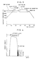
- Fig. 4 is an impurity density profile in a base region of the bipolar transistor
- Fig. 5 is a graph showing the relation between a boron peak density and an impurity gas application condition.
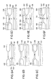
- Figs. 6A - 6F are a process step diagram of a PNP bipolar transistor.
- Figs. 1A - 1F are a process step diagram of an NPN bipolar transistor.
- a collector region 2 is formed on a semiconductor substrate 1 composed of silicon.
- the collector region 2 has a double layer structure comprised of a first layer 3 of N + type and a second layer 4 of N type.
- the N + type first layer 3 contains a high density of N type diffused impurity in order to reduce collector-series resistance of a bipolar transistor.
- the N type second layer 4 is used to form a PN junction.
- a field oxide film 5 is formed on the collector region 2 so as to isolate individual bipolar transistors from each other.
- the field oxide film 5 can be formed, for example, by means of selective thermal oxidation.
- the field oxide film 5 is provided to surround a device region in which one bipolar transistor is fabricated.
- the collector region 2 is cleaned over its surface, and thereafter is deposited with a semiconductor film layer 6 composed of silicon.
- the silicon semiconductor film layer 6 has a significantly small thickness since a base region is to be formed therein in later step.
- the deposition of the semiconductor film layer 6 can be carried out by, for example, molecular layer epitaxy.
- a semiconductor film layer 6 of silicon single crystal can be formed on the collector region 2.
- the surface of semiconductor film layer 6 is cleaned to expose an active surface.
- the substrate 1 is applied with a gas such as diborane which contains an impurity component of boron to form an impurity adsorption layer 7 composed of boron element or boron compound.
- the amount of the adsorbed impurity can be appropriately set by controlling gas pressure of diborane, application time interval and substrate temperature.
- the adsorbed impurity is diffused into the semiconductor film layer 6.
- the diffusion is carried out by heating the substrate.
- the substrate temperature and heating time interval are suitably set so as to substantially uniformly distribute the impurity boron to form a base region 8.
- an oxide layer 9 is disposed over the substrate surface except each device region.
- the oxide layer 9 is formed by means of chemical vapor deposition of silicon dioxide and etching thereof.
- a silicon semiconductor film layer 10 is deposited in a window surrounded by the oxide layer 9. This silicon semiconductor film layer 10 is formed by means of epitaxial growth or chemical vapor deposition.
- an N type impurity is introduced into the silicon semiconductor film layer 10 to form an emitter region 11.
- the N type impurity such as arsenic is doped, for example, by means of ion implantation.
- a source gas containing an N type impurity component may be applied to an active surface of the semiconductor film layer 10 to form an N type impurity adsorption layer, and thereafter diffusion treatment is conducted to form an emitter region.
- Fig. 2 shows a production apparatus operable to carry out continuously the sequential steps of deposition, cleaning, adsorption and diffusion according to the invention.
- the apparatus is comprised of a main chamber 12 made of quartz, in which is disposed a silicon semiconductor substrate 1 formed with the collector region 2 and the field oxide film 5.
- a temperature of the substrate 1 is held at a predetermined degree by controlling a heating system 13 using an infrared lamp heating or resistance heating.
- the chamber 12 can be evacuated at high vacuum by means of a high power vacuum system 14 comprised of plural pumps including a main pump in the form of a turbo molecular pump.
- the vacuum degree of chamber 12 is continuously monitored by a vacuum gage 15.
- the silicon substrate 1 is transported by means of a transportation mechanism 18 to the main chamber 12 from a loading chamber 17 through a gate valve 16a which is held open during the transportation.
- the loading chamber 17 is normally evacuated in high vacuum by means of a vacuum system 19 through a gate valve 16b which is held open except during the loading of silicon semiconductor substrate 1 into the loading chamber 17 and the transportation thereof.
- a gas supply source 21 is connected to the main chamber 12 through a gas flow control system 20.
- the gas supply source 21 has a plurality of bottles for storing various gas materials such as hydrogen, diborane and dichlorosilane needed for the sequential treatments.
- the gas flow control system 20 is operated to control gas species, pressure and application time interval during the course of gas charging from the gas supply source 21 to the chamber 12.
- Fig. 3 is an actual process sequence chart of the above described sequential treatments.
- the horizontal axis indicates time, and the vertical axis indicates substrate temperature in the chart.
- the substrate temperature is raised and stabilized. Thereafter, the surface of previously formed collector region is cleaned if desired. Then, the substrate temperature is slightly lowered and a semiconductor film layer is deposited on the collector region by epitaxial growth. Next, cleaning treatment is effected to a surface of the deposited semiconductor film layer to expose an active surface. Thereafter, an impurity adsorption layer is formed by mean of the inventive method. Lastly, annealing is carried out to diffuse the impurity in the impurity adsorption layer into the semiconductor film layer to form a base region.
- the silicon substrate formed with the base region is cooled to the room temperature and is taken out from the vacuum chamber 12 to proceed to following steps.
- the cleaning treatment may be eliminated before introduction of impurity gas, because the surface of the epitaxial growth layer is held active and is not covered by a natural oxide film in high vacuum state.
- the deposition step is carried out such that the substrate temperature is raised to 850°C and a surface of the collector region is cleaned if desired, and then the substrate temperature is lowered to 825°C, and thereafter a silicon semiconductor film layer is deposited by epitaxial growth technology.
- the epitaxial growth is conducted such that a source gas such as dichloro silane ( SiH2Cl2 ) or silane ( SiH4 ) is introduced into the main chamber 12 to effect so-called molecular layer epitaxy.
- This technology is effective to control the thickness of the semiconductor deposition layer by molecular layer order so as to accurately set a desired film thickness.
- This molecular epitaxy technology is disclosed, for example, in Japanese Patent Application Laid-open No. 153978/1984.
- the silicon single crystal film may be deposited by means of molecular beam epitaxy or chemical vapor deposition other than the molecular layer epitaxy.
- the cleaning treatment is applied to the deposited semiconductor film layer surface.
- This cleaning is carried out such that background pressure is set below 1 X 10 ⁇ 4Pa in the main chamber and the substrate temperature is held at, for example, 825°C, and then hydrogen gas is introduced into the chamber.
- the hydrogen gas is charged for a predetermined time interval so as to raise the chamber pressure to, for example, 1.3 x 10 ⁇ 5Pa.
- the cleaning treatment does not need necessarily the introduction of hydrogen gas, but the silicon substrate 1 may be simply placed in the highly vacuumed chamber while heating so as to effect the cleaning. Otherwise, when carrying out formation of an impurity adsorption layer in the same chamber immediately after the epitaxial growth of the semiconductor film layer, the cleaning treatment may be eliminated because the surface of the semiconductor film layer is maintained chemically active.
- an adsorption layer containing boron, element or boron compound is formed on the active surface of the silicon semiconductor film layer.
- diborane gas ( B2H6 ) containing boron is applied to the surface of the silicon substrate 1.
- the diborane gas dilluted with nitrogen carrier gas at 5% is introduced into the chamber for a predetermined time interval so as to fill the chamber at 1.3 X 10 ⁇ 2Pa of the internal pressure to thereby form the boron-containing adsorption layer.
- the diffusion treatment is carried out such that the diborane gas is stopped after formation of the impurity adsorption layer, and the substrate is annealed in vacuum to effect solid-phase diffusion of the boron from a diffusion source in the form of the adsorption layer. Concurrently, the diffused impurity atoms are activated in the silicon film layer.
- Fig. 4 shows an impurity diffusion density profile in the thus obtained base region.
- This profile is obtained by a secondary ion mass-spectrometer.
- a surface of the sample substrate is coated by an amorphous silicon layer in order to improve analysis accuracy on the sample surface. Therefore, in the Fig. 4 profile, the original surface level of the semiconductor film layer diffused with the impurity is indicated at a boundary between the amorphous silicon layer and the semiconductor film layer.
- the semiconductor film layer, i.e., epitaxial layer is uniformly doped with the impurity boron as shown in the profile.
- the impurity density profile steeply falls at a PN junction region between the lower collector region and the upper base region.
- the impurity diffusion is accurately controllably effected to the significantly thin epitaxial layer while regulating the impurity distribution profile in the depth direction.
- Fig. 5 is a graph showing the relation between the boron peak density in the base region, and the application pressure (P1, P2, P3) and application time interval of diborane gas. As shown in the graph, the higher the application pressure of diborane gas, the more the boron peak density. The longer the application time interval, also the more the boron peak density. In this manner, by suitably setting the application condition of diborane gas, the boron impurity concentration can be controlled in the base region.
- the P type impurity of boron is diffused into the silicon semiconductor film layer so as to form a P type base region of NPN bipolar transistor.
- the doping of P type impurity can be effected with using various source gases of III-group element compound such as trimethyl gallium (TMG) and boron trichloride( BCl3 ) besides the above described diborane gas.
- TMG trimethyl gallium
- BCl3 boron trichloride
- the substrate temperature is set to 825°C in the embodiment. According to the inventors' study, the substrate temperature should be set in the range from 800°C to 1200°C optimumly in conjunction with the background pressure and ambient gas species for the surface cleaning treatment. The substrate temperature should be preferably set in the range from 400°C to 950°C for the formation of impurity adsorption film. Further, the substrate temperature should be preferably set in the range from 800°C to 1100°C for the epitaxial growth of the semiconductor film layer.
- an impurity adsorption layer is directly formed on a semiconductor film layer deposited on a collector region, and solid-phase diffusion is effected from a diffusion source in the form of the adsorption layer so as to intensively and limitatively dope the impurity into the semiconductor film layer to thereby form therein a base region. Consequently, the thickness of the base region can be considerably reduced as compared to the prior art, thereby advantageously increasing operating speed of bipolar transistor.
- a collector region 102 is formed on a semiconductor substrate 101 composed of silicon.
- the collector region 102 has a double layer structure composed of a first diffusion layer 103 doped with high density of P type impurity and a second diffusion layer 104 doped with moderate density of the same P type impurity.
- the high density first diffusion layer 103 is provided to reduce collector-series resistance of a bipolar transistor, and the upper second diffusion layer 104 of P type is provided to form a PN junction.
- a field oxide film 105 is formed on the collector region 102. This field oxide film 105 is provided to isolate from each other a plurality of bipolar transistors integrated on the semiconductor substrate 101.
- the field oxide film 105 surrounds each device region.
- the field oxide film 105 is formed by, for example, selective thermal oxidation.
- the collector region 102 is covered by a first semiconductor film layer 106 composed of silicon.
- This first semiconductor film layer 106 is deposited by, for example, epitaxial growth or chemical vapor deposition of silicon.
- an impurity of N type is introduced into the first semiconductor film layer 106 to form a base region 107.
- the introduction of N type impurity is, for example, carried out by ion implantation to dope impurity of arsenic.
- an oxide film 108 is formed on the base region 107.
- the oxide film 108 is arranged to surround each device region at a position corresponding to the field oxide film 105.
- a second semiconductor film layer 109 is deposited on the device region surrounded by the oxide film 108.
- the second semiconductor film layer 109 is formed by epitaxial growth or chemical vapor deposition of silicon in manner similar to the first semiconductor film layer 106.
- the second semiconductor film layer 109 has a film thickness greater than that of the first semiconductor film layer in which is formed the base region since an emitter region is to be formed in the second semiconductor film layer 109.
- a surface of the second semiconductor film layer 109 is cleaned to expose an active silicon surface.
- the active surface is applied with an impurity gas of diborane having a P type impurity component of boron to form an impurity adsorption layer 110.
- Amount of the adsorbed impurity in impurity adsorption layer 110 is suitably set by controlling pressure and application time interval of the impurity gas of diborane.
- This impurity adsorption layer 110 is firmly and stably deposited on the active surface of the second semiconductor film layer 109. If an active surface is reserved after completion of the deposition of the second semiconductor film layer 109 and the formation of impurity adsorption film 110 is effected immediately, a particular cleaning treatment may be eliminated.
- solid-phase diffusion is carried out from a diffusion source composed of the deposited impurity adsorption layer 110 into the second semiconductor film layer 109 to form an emitter region 111.
- the diffusion of this P type impurity is limited within the emitter region 111 and is effected according to a doping amount more than a predetermined value. For this, an amount of impurity in the adsorption layer 110 must be optimumly set.
- the setting of the adsorption amount is controlled by adjusting pressure and application time interval of the impurity gas as described before.
- the base region is doped with the impurity by ion implantation in the above described embodiment; however, an impurity gas containing an N type impurity component may be utilized to form an adsorption layer of N type impurity, and solid-phase diffusion may be carried out from a diffusion source composed of this adsorption layer so as to form an N type base region.
- an impurity adsorption layer is deposited on an emitter region, and solid-phase diffusion is carried out from the adsorption layer so as to introduce an impurity, hence the impurity diffusion distribution cannot be affected in the base region which is formed under the emitter region.
Landscapes
- Bipolar Transistors (AREA)
Applications Claiming Priority (4)
| Application Number | Priority Date | Filing Date | Title |
|---|---|---|---|
| JP1313724A JPH03173437A (ja) | 1989-12-01 | 1989-12-01 | バイポーラトランジスタの製造方法 |
| JP313725/89 | 1989-12-01 | ||
| JP1313725A JPH03173438A (ja) | 1989-12-01 | 1989-12-01 | バイポーラトランジスタの製造方法 |
| JP313724/89 | 1989-12-01 |
Publications (2)
| Publication Number | Publication Date |
|---|---|
| EP0430274A2 true EP0430274A2 (de) | 1991-06-05 |
| EP0430274A3 EP0430274A3 (en) | 1993-03-24 |
Family
ID=26567681
Family Applications (1)
| Application Number | Title | Priority Date | Filing Date |
|---|---|---|---|
| EP19900122947 Withdrawn EP0430274A3 (en) | 1989-12-01 | 1990-11-30 | Method of producing bipolar transistor |
Country Status (3)
| Country | Link |
|---|---|
| US (1) | US5925574A (de) |
| EP (1) | EP0430274A3 (de) |
| CA (1) | CA2031253A1 (de) |
Cited By (4)
| Publication number | Priority date | Publication date | Assignee | Title |
|---|---|---|---|---|
| US5753530A (en) * | 1992-04-21 | 1998-05-19 | Seiko Instruments, Inc. | Impurity doping method with diffusion source of boron-silicide film |
| FR2803091A1 (fr) * | 1999-12-22 | 2001-06-29 | St Microelectronics Sa | Procede de dopage de la base extrinseque d'un transistor bipolaire |
| DE102004013478A1 (de) * | 2004-03-18 | 2005-10-06 | Austriamicrosystems Ag | Verfahren zur Herstellung eines Bipolartransistors mit verbessertem Basisanschluss |
| US8158451B2 (en) | 2008-12-29 | 2012-04-17 | Imec | Method for manufacturing a junction |
Families Citing this family (39)
| Publication number | Priority date | Publication date | Assignee | Title |
|---|---|---|---|---|
| US6673673B1 (en) * | 1997-04-22 | 2004-01-06 | Samsung Electronics Co., Ltd. | Method for manufacturing a semiconductor device having hemispherical grains |
| US6620723B1 (en) | 2000-06-27 | 2003-09-16 | Applied Materials, Inc. | Formation of boride barrier layers using chemisorption techniques |
| US7732327B2 (en) | 2000-06-28 | 2010-06-08 | Applied Materials, Inc. | Vapor deposition of tungsten materials |
| US7101795B1 (en) | 2000-06-28 | 2006-09-05 | Applied Materials, Inc. | Method and apparatus for depositing refractory metal layers employing sequential deposition techniques to form a nucleation layer |
| US7964505B2 (en) | 2005-01-19 | 2011-06-21 | Applied Materials, Inc. | Atomic layer deposition of tungsten materials |
| US7405158B2 (en) | 2000-06-28 | 2008-07-29 | Applied Materials, Inc. | Methods for depositing tungsten layers employing atomic layer deposition techniques |
| US6551929B1 (en) | 2000-06-28 | 2003-04-22 | Applied Materials, Inc. | Bifurcated deposition process for depositing refractory metal layers employing atomic layer deposition and chemical vapor deposition techniques |
| US6825447B2 (en) * | 2000-12-29 | 2004-11-30 | Applied Materials, Inc. | Apparatus and method for uniform substrate heating and contaminate collection |
| US20020083897A1 (en) * | 2000-12-29 | 2002-07-04 | Applied Materials, Inc. | Full glass substrate deposition in plasma enhanced chemical vapor deposition |
| US6765178B2 (en) | 2000-12-29 | 2004-07-20 | Applied Materials, Inc. | Chamber for uniform substrate heating |
| US6998579B2 (en) | 2000-12-29 | 2006-02-14 | Applied Materials, Inc. | Chamber for uniform substrate heating |
| US6413844B1 (en) * | 2001-01-10 | 2002-07-02 | Asm International N.V. | Safe arsenic gas phase doping |
| US6951804B2 (en) | 2001-02-02 | 2005-10-04 | Applied Materials, Inc. | Formation of a tantalum-nitride layer |
| US6660126B2 (en) | 2001-03-02 | 2003-12-09 | Applied Materials, Inc. | Lid assembly for a processing system to facilitate sequential deposition techniques |
| US6878206B2 (en) | 2001-07-16 | 2005-04-12 | Applied Materials, Inc. | Lid assembly for a processing system to facilitate sequential deposition techniques |
| US6734020B2 (en) | 2001-03-07 | 2004-05-11 | Applied Materials, Inc. | Valve control system for atomic layer deposition chamber |
| US7211144B2 (en) | 2001-07-13 | 2007-05-01 | Applied Materials, Inc. | Pulsed nucleation deposition of tungsten layers |
| US7085616B2 (en) | 2001-07-27 | 2006-08-01 | Applied Materials, Inc. | Atomic layer deposition apparatus |
| US7049226B2 (en) | 2001-09-26 | 2006-05-23 | Applied Materials, Inc. | Integration of ALD tantalum nitride for copper metallization |
| US6936906B2 (en) | 2001-09-26 | 2005-08-30 | Applied Materials, Inc. | Integration of barrier layer and seed layer |
| US6916398B2 (en) | 2001-10-26 | 2005-07-12 | Applied Materials, Inc. | Gas delivery apparatus and method for atomic layer deposition |
| US6729824B2 (en) | 2001-12-14 | 2004-05-04 | Applied Materials, Inc. | Dual robot processing system |
| US6620670B2 (en) | 2002-01-18 | 2003-09-16 | Applied Materials, Inc. | Process conditions and precursors for atomic layer deposition (ALD) of AL2O3 |
| US6911391B2 (en) | 2002-01-26 | 2005-06-28 | Applied Materials, Inc. | Integration of titanium and titanium nitride layers |
| US6998014B2 (en) | 2002-01-26 | 2006-02-14 | Applied Materials, Inc. | Apparatus and method for plasma assisted deposition |
| US6827978B2 (en) | 2002-02-11 | 2004-12-07 | Applied Materials, Inc. | Deposition of tungsten films |
| US6833161B2 (en) | 2002-02-26 | 2004-12-21 | Applied Materials, Inc. | Cyclical deposition of tungsten nitride for metal oxide gate electrode |
| US6825134B2 (en) * | 2002-03-26 | 2004-11-30 | Applied Materials, Inc. | Deposition of film layers by alternately pulsing a precursor and high frequency power in a continuous gas flow |
| US7439191B2 (en) | 2002-04-05 | 2008-10-21 | Applied Materials, Inc. | Deposition of silicon layers for active matrix liquid crystal display (AMLCD) applications |
| US6846516B2 (en) | 2002-04-08 | 2005-01-25 | Applied Materials, Inc. | Multiple precursor cyclical deposition system |
| US6720027B2 (en) | 2002-04-08 | 2004-04-13 | Applied Materials, Inc. | Cyclical deposition of a variable content titanium silicon nitride layer |
| US6869838B2 (en) * | 2002-04-09 | 2005-03-22 | Applied Materials, Inc. | Deposition of passivation layers for active matrix liquid crystal display (AMLCD) applications |
| US6875271B2 (en) | 2002-04-09 | 2005-04-05 | Applied Materials, Inc. | Simultaneous cyclical deposition in different processing regions |
| US20030194825A1 (en) * | 2002-04-10 | 2003-10-16 | Kam Law | Deposition of gate metallization for active matrix liquid crystal display (AMLCD) applications |
| US7279432B2 (en) | 2002-04-16 | 2007-10-09 | Applied Materials, Inc. | System and method for forming an integrated barrier layer |
| US6821563B2 (en) | 2002-10-02 | 2004-11-23 | Applied Materials, Inc. | Gas distribution system for cyclical layer deposition |
| US7262133B2 (en) | 2003-01-07 | 2007-08-28 | Applied Materials, Inc. | Enhancement of copper line reliability using thin ALD tan film to cap the copper line |
| US7211508B2 (en) | 2003-06-18 | 2007-05-01 | Applied Materials, Inc. | Atomic layer deposition of tantalum based barrier materials |
| US6933202B1 (en) * | 2004-04-09 | 2005-08-23 | Newport Fab, Llc | Method for integrating SiGe NPN and vertical PNP devices on a substrate and related structure |
Family Cites Families (18)
| Publication number | Priority date | Publication date | Assignee | Title |
|---|---|---|---|---|
| NL6501786A (de) * | 1964-02-26 | 1965-08-27 | ||
| JPS5145951B2 (de) * | 1972-06-07 | 1976-12-06 | ||
| US4242691A (en) * | 1978-09-18 | 1980-12-30 | Mitsubishi Denki Kabushiki Kaisha | MOS Semiconductor device |
| JPS5674921A (en) * | 1979-11-22 | 1981-06-20 | Toshiba Corp | Manufacturing method of semiconductor and apparatus thereof |
| US4345366A (en) * | 1980-10-20 | 1982-08-24 | Ncr Corporation | Self-aligned all-n+ polysilicon CMOS process |
| JPS57149770A (en) * | 1981-03-11 | 1982-09-16 | Mitsubishi Electric Corp | Manufacture of semiconductor device |
| JPH0766909B2 (ja) * | 1984-07-26 | 1995-07-19 | 新技術事業団 | 元素半導体単結晶薄膜の成長法 |
| JPS61292358A (ja) * | 1985-06-19 | 1986-12-23 | Fujitsu Ltd | Mis型電界効果トランジスタの製造方法 |
| DE3684539D1 (de) * | 1985-09-06 | 1992-04-30 | Philips Nv | Herstellungsverfahren einer halbleitervorrichtung. |
| US4791074A (en) * | 1986-08-29 | 1988-12-13 | Kabushiki Kaisha Toshiba | Method of manufacturing a semiconductor apparatus |
| JPH0639357B2 (ja) * | 1986-09-08 | 1994-05-25 | 新技術開発事業団 | 元素半導体単結晶薄膜の成長方法 |
| JPH07120635B2 (ja) * | 1986-12-26 | 1995-12-20 | 株式会社東芝 | 半導体装置の製造方法 |
| JPS62271475A (ja) * | 1987-04-03 | 1987-11-25 | Hitachi Ltd | 半導体装置 |
| US4861729A (en) * | 1987-08-24 | 1989-08-29 | Matsushita Electric Industrial Co., Ltd. | Method of doping impurities into sidewall of trench by use of plasma source |
| US4855258A (en) * | 1987-10-22 | 1989-08-08 | Ncr Corporation | Native oxide reduction for sealing nitride deposition |
| KR910009030B1 (ko) * | 1987-12-30 | 1991-10-28 | 후지쓰 가부시끼가이샤 | 얇은 접합의 형성방법 및 상기 얇은 접합을 갖는 반도체장치 |
| US4940505A (en) * | 1988-12-02 | 1990-07-10 | Eaton Corporation | Method for growing single crystalline silicon with intermediate bonding agent and combined thermal and photolytic activation |
| EP0413982B1 (de) * | 1989-07-27 | 1997-05-14 | Junichi Nishizawa | Dotierungsverfahren mittels einer adsorbierten Diffusionquelle |
-
1990
- 1990-11-30 EP EP19900122947 patent/EP0430274A3/en not_active Withdrawn
- 1990-11-30 CA CA002031253A patent/CA2031253A1/en not_active Abandoned
-
1992
- 1992-04-10 US US07/865,646 patent/US5925574A/en not_active Expired - Lifetime
Cited By (6)
| Publication number | Priority date | Publication date | Assignee | Title |
|---|---|---|---|---|
| US5753530A (en) * | 1992-04-21 | 1998-05-19 | Seiko Instruments, Inc. | Impurity doping method with diffusion source of boron-silicide film |
| FR2803091A1 (fr) * | 1999-12-22 | 2001-06-29 | St Microelectronics Sa | Procede de dopage de la base extrinseque d'un transistor bipolaire |
| DE102004013478A1 (de) * | 2004-03-18 | 2005-10-06 | Austriamicrosystems Ag | Verfahren zur Herstellung eines Bipolartransistors mit verbessertem Basisanschluss |
| US7618871B2 (en) | 2004-03-18 | 2009-11-17 | Austriamicrosystems Ag | Method for the production of a bipolar transistor comprising an improved base terminal |
| DE102004013478B4 (de) * | 2004-03-18 | 2010-04-01 | Austriamicrosystems Ag | Verfahren zur Herstellung eines Bipolartransistors mit verbessertem Basisanschluss |
| US8158451B2 (en) | 2008-12-29 | 2012-04-17 | Imec | Method for manufacturing a junction |
Also Published As
| Publication number | Publication date |
|---|---|
| US5925574A (en) | 1999-07-20 |
| CA2031253A1 (en) | 1991-06-02 |
| EP0430274A3 (en) | 1993-03-24 |
Similar Documents
| Publication | Publication Date | Title |
|---|---|---|
| EP0430274A2 (de) | Verfahren zur Herstellung von einem bipolaren Transistor | |
| US5527733A (en) | Impurity doping method with adsorbed diffusion source | |
| US4063967A (en) | Method of producing a doped zone of one conductivity type in a semiconductor body utilizing an ion-implanted polycrystalline dopant source | |
| US4966861A (en) | Vapor deposition method for simultaneously growing an epitaxial silicon layer and a polycrystalline silicone layer over a selectively oxidized silicon substrate | |
| US3664896A (en) | Deposited silicon diffusion sources | |
| US6043139A (en) | Process for controlling dopant diffusion in a semiconductor layer | |
| US5366922A (en) | Method for producing CMOS transistor | |
| US5338697A (en) | Doping method of barrier region in semiconductor device | |
| GB2368726A (en) | Selective epitaxial growth method in semiconductor device | |
| US5387545A (en) | Impurity diffusion method | |
| US5256162A (en) | Apparatus for forming shallow electrical junctions | |
| EP0438677A2 (de) | Vorrichtung zur Dotierung von Verunreinigungen | |
| JP2906260B2 (ja) | Pn接合素子の製造方法 | |
| JPS63166220A (ja) | 半導体装置の製造方法 | |
| EP0430168A2 (de) | Verfahren zur Dotierung von Grabenwänden eines Halbleiters | |
| US5874352A (en) | Method of producing MIS transistors having a gate electrode of matched conductivity type | |
| US6136673A (en) | Process utilizing selective TED effect when forming devices with shallow junctions | |
| EP0430166A2 (de) | Verfahren zur Dotierung von Halbleiterschichten und strukturierten Halbleiterstreifen | |
| EP0505877A2 (de) | Dotierungsverfahren mittels einer adsorbierten Diffusionsquelle | |
| JP2876414B2 (ja) | 拡散抵抗素子の製造方法 | |
| JP2928929B2 (ja) | 不純物ドーピング方法 | |
| EP0431616A2 (de) | Verfahren zur Herstellung von einem CMOS-Transistor | |
| JP2926344B2 (ja) | 電界効果トランジスタの製造方法 | |
| JP2934665B2 (ja) | 半導体装置の製造方法 | |
| JPH0590280A (ja) | 半導体装置の製造方法 |
Legal Events
| Date | Code | Title | Description |
|---|---|---|---|
| PUAI | Public reference made under article 153(3) epc to a published international application that has entered the european phase |
Free format text: ORIGINAL CODE: 0009012 |
|
| AK | Designated contracting states |
Kind code of ref document: A2 Designated state(s): DE FR GB |
|
| PUAL | Search report despatched |
Free format text: ORIGINAL CODE: 0009013 |
|
| AK | Designated contracting states |
Kind code of ref document: A3 Designated state(s): DE FR GB |
|
| 17P | Request for examination filed |
Effective date: 19930917 |
|
| 17Q | First examination report despatched |
Effective date: 19950807 |
|
| STAA | Information on the status of an ep patent application or granted ep patent |
Free format text: STATUS: THE APPLICATION IS DEEMED TO BE WITHDRAWN |
|
| 18D | Application deemed to be withdrawn |
Effective date: 19951219 |