EP0430279A2 - Si/SiGe-Bipolartransistor mit Heteroübergang unter Verwendung verbesserter Epitaxialscheidungstechniken und Verfahren zur Herstellung - Google Patents
Si/SiGe-Bipolartransistor mit Heteroübergang unter Verwendung verbesserter Epitaxialscheidungstechniken und Verfahren zur Herstellung Download PDFInfo
- Publication number
- EP0430279A2 EP0430279A2 EP90122968A EP90122968A EP0430279A2 EP 0430279 A2 EP0430279 A2 EP 0430279A2 EP 90122968 A EP90122968 A EP 90122968A EP 90122968 A EP90122968 A EP 90122968A EP 0430279 A2 EP0430279 A2 EP 0430279A2
- Authority
- EP
- European Patent Office
- Prior art keywords
- layer
- silicon
- window
- field oxide
- collector
- Prior art date
- Legal status (The legal status is an assumption and is not a legal conclusion. Google has not performed a legal analysis and makes no representation as to the accuracy of the status listed.)
- Withdrawn
Links
- 229910000577 Silicon-germanium Inorganic materials 0.000 title claims abstract description 67
- 238000004519 manufacturing process Methods 0.000 title claims abstract description 11
- 238000000151 deposition Methods 0.000 title claims description 36
- 239000000758 substrate Substances 0.000 claims abstract description 66
- 239000004065 semiconductor Substances 0.000 claims abstract description 22
- 238000000034 method Methods 0.000 claims description 42
- 229910021420 polycrystalline silicon Inorganic materials 0.000 claims description 29
- VYPSYNLAJGMNEJ-UHFFFAOYSA-N Silicium dioxide Chemical compound O=[Si]=O VYPSYNLAJGMNEJ-UHFFFAOYSA-N 0.000 claims description 28
- 229910052710 silicon Inorganic materials 0.000 claims description 22
- XUIMIQQOPSSXEZ-UHFFFAOYSA-N Silicon Chemical compound [Si] XUIMIQQOPSSXEZ-UHFFFAOYSA-N 0.000 claims description 20
- 239000010703 silicon Substances 0.000 claims description 20
- 235000012239 silicon dioxide Nutrition 0.000 claims description 14
- 239000000377 silicon dioxide Substances 0.000 claims description 14
- 239000000463 material Substances 0.000 claims description 6
- 150000004767 nitrides Chemical class 0.000 claims description 6
- LEVVHYCKPQWKOP-UHFFFAOYSA-N [Si].[Ge] Chemical compound [Si].[Ge] LEVVHYCKPQWKOP-UHFFFAOYSA-N 0.000 claims 22
- 230000008021 deposition Effects 0.000 description 24
- 230000008569 process Effects 0.000 description 18
- 229910052681 coesite Inorganic materials 0.000 description 12
- 229910052906 cristobalite Inorganic materials 0.000 description 12
- 238000005530 etching Methods 0.000 description 12
- 229910052682 stishovite Inorganic materials 0.000 description 12
- 229910052905 tridymite Inorganic materials 0.000 description 12
- 238000002955 isolation Methods 0.000 description 9
- 238000001459 lithography Methods 0.000 description 5
- 238000001465 metallisation Methods 0.000 description 5
- ZOXJGFHDIHLPTG-UHFFFAOYSA-N Boron Chemical compound [B] ZOXJGFHDIHLPTG-UHFFFAOYSA-N 0.000 description 4
- 229910052785 arsenic Inorganic materials 0.000 description 4
- RQNWIZPPADIBDY-UHFFFAOYSA-N arsenic atom Chemical compound [As] RQNWIZPPADIBDY-UHFFFAOYSA-N 0.000 description 4
- 230000015572 biosynthetic process Effects 0.000 description 4
- 229910052796 boron Inorganic materials 0.000 description 4
- OAICVXFJPJFONN-UHFFFAOYSA-N Phosphorus Chemical compound [P] OAICVXFJPJFONN-UHFFFAOYSA-N 0.000 description 3
- 230000008901 benefit Effects 0.000 description 3
- 238000009792 diffusion process Methods 0.000 description 3
- 229910052698 phosphorus Inorganic materials 0.000 description 3
- 239000011574 phosphorus Substances 0.000 description 3
- 238000000407 epitaxy Methods 0.000 description 2
- 239000007789 gas Substances 0.000 description 2
- 239000007943 implant Substances 0.000 description 2
- 230000003993 interaction Effects 0.000 description 2
- 230000003071 parasitic effect Effects 0.000 description 2
- 229920005591 polysilicon Polymers 0.000 description 2
- 125000006850 spacer group Chemical group 0.000 description 2
- 229910006990 Si1-xGex Inorganic materials 0.000 description 1
- 229910007020 Si1−xGex Inorganic materials 0.000 description 1
- 229910052581 Si3N4 Inorganic materials 0.000 description 1
- 229910045601 alloy Inorganic materials 0.000 description 1
- 239000000956 alloy Substances 0.000 description 1
- 238000006243 chemical reaction Methods 0.000 description 1
- 230000003749 cleanliness Effects 0.000 description 1
- 230000008878 coupling Effects 0.000 description 1
- 238000010168 coupling process Methods 0.000 description 1
- 238000005859 coupling reaction Methods 0.000 description 1
- 239000013078 crystal Substances 0.000 description 1
- 229910021419 crystalline silicon Inorganic materials 0.000 description 1
- 230000007423 decrease Effects 0.000 description 1
- 230000007547 defect Effects 0.000 description 1
- 230000000593 degrading effect Effects 0.000 description 1
- MROCJMGDEKINLD-UHFFFAOYSA-N dichlorosilane Chemical compound Cl[SiH2]Cl MROCJMGDEKINLD-UHFFFAOYSA-N 0.000 description 1
- 229910000078 germane Inorganic materials 0.000 description 1
- QUZPNFFHZPRKJD-UHFFFAOYSA-N germane Chemical compound [GeH4] QUZPNFFHZPRKJD-UHFFFAOYSA-N 0.000 description 1
- 229910052986 germanium hydride Inorganic materials 0.000 description 1
- 238000010438 heat treatment Methods 0.000 description 1
- 238000002513 implantation Methods 0.000 description 1
- 238000011065 in-situ storage Methods 0.000 description 1
- 238000002347 injection Methods 0.000 description 1
- 239000007924 injection Substances 0.000 description 1
- 238000001451 molecular beam epitaxy Methods 0.000 description 1
- 230000010355 oscillation Effects 0.000 description 1
- 239000000126 substance Substances 0.000 description 1
- 230000008719 thickening Effects 0.000 description 1
Images


Classifications
-
- H—ELECTRICITY
- H10—SEMICONDUCTOR DEVICES; ELECTRIC SOLID-STATE DEVICES NOT OTHERWISE PROVIDED FOR
- H10D—INORGANIC ELECTRIC SEMICONDUCTOR DEVICES
- H10D10/00—Bipolar junction transistors [BJT]
- H10D10/01—Manufacture or treatment
- H10D10/021—Manufacture or treatment of heterojunction BJTs [HBT]
-
- H—ELECTRICITY
- H10—SEMICONDUCTOR DEVICES; ELECTRIC SOLID-STATE DEVICES NOT OTHERWISE PROVIDED FOR
- H10D—INORGANIC ELECTRIC SEMICONDUCTOR DEVICES
- H10D10/00—Bipolar junction transistors [BJT]
- H10D10/80—Heterojunction BJTs
- H10D10/821—Vertical heterojunction BJTs
- H10D10/891—Vertical heterojunction BJTs comprising lattice-mismatched active layers, e.g. SiGe strained-layer transistors
Definitions
- This invention relates to Si/Si 1-x Ge x heterojunction bipolar transistors, particularly, high speed, small size, low junction capacitance transistors.
- Advanced silicon bipolar transistors suffer from the competing requirements for thin base regions to obtain high unity-gain cutoff frequencies and low-resistance base regions to achieve high maximum oscillation frequencies using a heterojunction transistor (HBT) (eg. Si/SiGe) relaxes the coupling between f L , the unity gain cutoff frequency, and base resistance.
- HBT heterojunction transistor
- the base doping can be increased without degrading the emitter injection efficiency, thus, improving the speed, size, and capacitance of bipolar transistors.
- Si and SiGe layers are deposited either selectively or non-selectively by either limited reaction processing, or a more typical process, each of which have been disclosed in the prior art.
- the Si and Ge bearing gases used are dichlorosilane and germane, although other Si and Ge containing gases can be used.
- the temperatures that are used are those typically used in the processing of Si semiconductor devices, typically around 1000 degrees C.
- the SiGe layer is established at typically 625 degrees C, and the post SiGe processing of the semiconductor device is done at as low a temperature as practical, typically in the range of 800 to 850 degrees C.
- the percentage of Ge in the alloy layer is dictated largely by the application of the device, and is generally in the range of 10 - 30 % by atomic fraction.
- the present invention includes both a method of making, and a low capacitance, high speed, heterojunction semiconductor device.
- a device includes a p type Si substrate with an n type subcollector layer on top of the substrate, and a field oxide layer with a window therethrough to define the active region of the semiconductor device over a portion of the subcollector layer with a collector layer on top of the subcollector layer on the substrate or in the window surrounded by the field oxide.
- a p type SiGe layer is deposited non-selectively over the field oxide layer and on the collector layer in window defining the active region.
- a dielectric layer is deposited over the SiGe layer.
- there are metalized contacts extending through windows in the dielectric layer above the SiGe layer and the field oxide layer making contact with the SiGe layer through one window and the subcollector layer through another window.
- the preferred embodiments of the present invention includes both a method of making, and a low capacitance, high speed, heterojunction transistor.
- a device includes the above discussed layers with a second n-type Si layer deposited non-selectively over the SiGe layer. The dielectric layer is then over the second Si layer. And, finally, there are metalized contacts extending through windows in the dielectric layer, an emitter contact above the active region making contact with the second Si layer through one window, a base contact making contact with SiGe layer above the field oxide layer through a second window, and a collector contact through the field oxide layer making contact to the subcollector layer through a third window outside of the active region.
- Fig. 1 is a cross-sectional schematic view of a general transistor structure that is representative of each of the embodiments of the present invention.
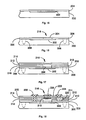
- Figs. 2 - 10 illustrate the steps for producing a high speed transistor of the first embodiment of the present invention in cross-sectional views of a semiconductor substrate for a single transistor.
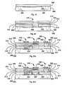
- Figs. 11 - 14 illustrate the steps for producing a high speed transistor of the second embodiment of the present invention in cross-sectional views of a semiconductor substrate for a single transistor.
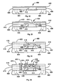
- Figs. 15 - 18 illustrate the steps for producing a high speed transistor of the third embodiment of the present invention in cross-sectional views of a semiconductor substrate for a single transistor.
- Figs. 19 - 21 illustrate the steps for producing a high speed transistor of the fourth embodiment of the present invention in cross-sectional views of a semiconductor substrate for a single transistor.
- Figs. 22-25 illustrate the steps for producing a high speed transistor of the fifth embodiment of the present invention in cross-sectional views of a semiconductor substrate for a single transistor.
- the Si or SiGe only deposits on the exposed portions of the Si substrate, not on the dielectric.
- Si or SiGe is deposited on both the on exposed Si and on the dielectric layer. Over exposed Si the deposited Si or SiGe layer will take the form of a single crystal (epitaxial deposition), and over the dielectric, the Si or SiGe layer will take the form of a polycrystalline layer.
- n + substrate is used beneath the n + collector layer, instead of a p substrate with an n + buried layer (subcollector).
- Fig. 1 A representative transistor of the type of the embodiments disclosed below is shown in Fig. 1.
- the base connection is separated from the underlying collector region by a layer of SiO2, with its low relative permittivity.
- the collector-base junction area is approximately the same as the emitter-base junction area; the base-collector capacitance then decreases by approximately 70% (for an oxide thickness of 500 nm), significantly increasing f T and f max .
- advanced selective or mixed epitaxial deposition is needed.
- the SiGe layer can then be deposited on a partially fabricated structure, with the buried subcollector possibly the n' Si collector region and the device isolation already in place. To explore this requirement, the ability to deposit SiGe selectively using SiH2CL2 and GeH4 has been investigated.
- An oxide mask is used to define the regions on which deposition occurs.
- a silicon collector layer may be first grown, followed by in-situ deposition of the SiGe layer.
- the deposition of the silicon layer can be selective.
- the deposition of the SiGe can be selective.
- the SiGe deposition can be nonselective (or mixed).
- the measured value of f T was approximately 29 GHz.
- Advanced deposition on a partially processed wafer should markedly reduce parasitic elements and increase f T .
- a transistor of the first embodiment of the present invention is shown in Figs. 2-10a and b. At various points in the following discussion, alternative techniques are discussed but not always shown in the figures. The steps shown in the figures are the preferred steps but by no means are they the only steps that may be utilized at any particular point.
- the transistor of the first embodiment of the present invention is produced by a combination of standard and mixed deposition techniques.
- a semiconductor substrate 10 typically with a selected (100) crystalline orientation, of a p conductivity type Si.
- the surface of substrate 10 is initially prepared by adding an n + layer 12 on the top surface of substrate 10 with an n - layer 14 on top of layer 12.
- Layer 12 can be either grown epitaxially, or it can be implanted and diffused into the top surface of substrate 10 to form the subcollector layer 12.
- the implant and diffusion technique is probably the technique of choice here; however, epitaxy also will produce an acceptable result.
- the n - layer 14 is then grown epitaxially on top of layer 12.
- the next step in the process is the etching of the isolation trench 16 well below the top surface of substrate 10 through the n + layer into the p - substrate.
- An isolation trench 16 is provided to encircle each site on the wafer where a transistor is to be fabricated and there is to be more than one transistor on the completed integrated circuit. Isolation trenches 16 minimize the interaction between the various transistors through the substrate.
- Trench 16 is produced by conventional means, for example by growing or depositing an oxide layer 15 on layer 14 and removing it by lithography and etching, from the areas where the trench 16 is to be formed. That is followed by the etching of the substrate 10 through the holes in the oxide layer 15. By proper control of the etch process, the walls of trenches 16 will be substantially orthogonal to the surface of substrate 10.
- a thicker SiO2 layer 18 is deposited on substrate 10 combining with layer 15 and also filling trenches 16.
- SiO2 can be formed on the bottom and sides of trenches 16, and then trenches 16 can be filled with polycrystalline Si.
- the polycrystalline Si is then etched from all areas but the trenches, and a field SiO2 oxide layer can be regrown over the trenches so that an oxide layer covers the entire surface of the substrate 10.
- a p + type polycrystalline Si layer 20 is then deposited on oxide layer 18 with a dielectric layer 22, typically of SiO2, formed over poly Si layer 20.
- a lithography technique is used to etch through layers 18-22 to expose a portion of the surface of layer 14 in the area which will become the active region 24 of the transistor when completed.
- a dielectric layer 26 say a thermal oxide
- a dielectric layer 26 over the entire substrate which results in the slight thickening of layer 22 outside of active region 24 and the application of a dielectric layer 26 on layer 14 in the active emitter region 24.
- Layers 26 and 22 each act as an etch stop in a later step. That is followed by the deposition of a p + type polycrystalline Si layer 28 over the entire substrate including the cavity (bottom and sides) of the active region 24.
- the polysilicon layer 28 is anisotropically etched from the horizontal surfaces of layers 22 and 26.
- the dielectric layers 22 and 26 in this step act as the etch stops mentioned above. This results in the vertical side-walls of well 24 being poly Si.
- Dielectric layers 26 in the active region 24 and layer 22 in the field region are then removed by etching.
- dielectric layer 26 and possibly layer 22 may be omitted. If layer 26 is omitted, boron may be diffused from layer 28 on the sidewalls of well 24 into the intersection of the poly Si of layer 28 and layer 14 on the surface of substrate 10 which causes the p + material to extend below the top of the n - epitaxial Si layer 14. This can potentially reduce series resistance in the base and also lower junction leakage.
- layers 22 and 28 can be omitted so that no polysilicon is formed on the sidewalls of the dielectric 18.
- Fig. 8 With the mixed deposition of a p + SiGe layer 32 over the poly Si layers 20 and 28 and the exposed single crystalline Si of layer 14 of the substrate 10. That is followed by the mixed deposition of an n - Si layer 34 on layer 32.
- the deposition of both of layers 32 and 34 is preferably performed by chemical vapor depositon, but can be formed by other techniques such as molecular beam epitaxy.
- the SiGe layer 32 will be the base layer. From this point in the process there are many different techniques that can be utilized, and the order in which those steps are performed is not critical.
- the next step is the optional formation of SiO2 36 the sidewalls of well 24 as spacers.
- the regions outside well 24 and spacers may be doped P + type by boron implantation.
- an SiO2 layer 38 is shown having been formed over the entire surface of the substrate 10, including the bottom and sidewalls of well 24.
- Fig. 10a shows oxide layer 38 having been opened in the emitter region 24, the base contact region 40 and the collector contact region 42, typically by a combination of lithography and etching.
- Emitter region 24 is etched to layer 34 which may be doped n + at least near its surface, the base contact region is etched to a p-type surface, and the collector contact region is etched to an n-type region contacting layer 12 or to layer 12 itself.
- the emitter, base and collector contact regions are each metallized to create electrical interconnection contacts 44, 46 and 48, respectively.
- Fig. 10b shows an alternative method of making contact to the bass and collector regions of the transistor of the present invention for the first embodiment.
- the base contact instead of etching down to layer 32 through the window that defines the location of the base contact, boron can be doped in layer 34 through the base contact window in dielectric layer 38. This then creates a localized p type region 47 surrounded by layer 34 that extends through layer 34 to p type SiGe layer 32 Base contact 46 is then metalized as above.
- the collector connection can be done other than by etching through all of the layers to subcollector layer 12.
- a well 21 could have been opened through dielectric layer 18 so that layer 20 also filled well 21.
- dielectric layer 22 was developed on poly Si layer 20
- a window above well 21 could have been opened and the poly Si that extends down to sub-collector layer 12 doped with arsenic or phosphorus to create a localized n type region.
- arsenic or phosphorus could again be used to dope layer 32 n type through n type layer 34.
- the collector metalization can simply be made to layer 34 since an n type path through the structure to the sub-collector layer 12 was developed as the device was produced.
- An advantage of the configuration of the first embodiment is that significant heat treatment is not necessary after formation of SiGe layer 32 in that nonselective Si deposition is necessary.
- the base-collector junction near the sidewalls of the device may extend below the SiGe layer to reduce sidewall leakage.
- the second embodiment of the present invention is a transistor produced by the steps depicted in Figs. 11-14.
- a semiconductor substrate 100 with a selected (100) crystalline orientation of a p - conductivity type Si is initially prepared by adding a sub-collector n + region 102 in the top surface. Region 102 is implanted and diffused into a portion of the top surface of substrate 100, or it could be formed epitaxially, as discussed in connection with Fig 2. Isolation trenches 104 are also formed to define the transistor regions on substrate 100 in the same manner as discussed above in the development of a transistor of the first embodiment. Next a field oxide layer 106 is grown over the top surface of substrate 100, including region 102.
- an active region well 108 is opened above one end of the sub-collector region 102 by means of lithography and etching techniques that are well known in the art. That may be followed by the formation of a nitride Si3N4 layer 110 on the surface of the oxide layer 106, including the side walls of well 108. To maintain the cleanliness of the critical surface between each of the next three steps, those three steps can be performed in one reactor cycle. First an n - type Si layer 112 is selectively, epitaxially grown in well 108. Layer 112 will become the collector layer. The thickness of layer 112 is typically less than or equal to the thickness of oxide layer 106.
- a p + type SiGe layer 114 is deposited non-selectively in mixed form over the entire surface of substrate 100.
- the portion of layer 114 that is substantially above layer 112 will grow epitaxially and thus have a single crystalline structure, and the portion of layer 114 above the oxide or nitride layer will have a polycrystalline structure.
- Layer 114 also, will become the base layer.
- an n - type Si layer 116 is nonselectively deposited in mixed form on the SiGe layer 114, and this layer will become the emitter layer. Similar to layer 114, layer 116 grows epitaxially with a single crystalline structure above the single crystalline portion of layer 114, and the remainder of layer 116 has a polycrystalline structure.
- the polycrystalline portions and a small portion of the epitaxial portions near the polycrystalline portions of layers 114 and 116 are counter doped with boron to become p + type material, or more heavily p + type, indicated as layer 118.
- both layer 114 and layer 118 are each p + type material, thus layer 118 becomes a reasonably low resistance base contact layer of the transistor. This structure limits the thickness of the base layer 118 to the combined thickness of layers 114 and 116.
- Fig. 14 illustrates one of the possible final forms that result from one of the step sequences that may be used to accomplish this.
- a dielectric layer 120 is formed over layers 116 and 118.
- a window is then opened to establish the collector contact at 124.
- the well for this contact may be etched through layers 120, 118, 110 and 106 to allow electrical connection to sub-collector region 102 and thereby to collector layer 112.
- a contact may be made to an n-type region previously formed extending from the surface to the n + region 102 in the conventional manner.
- a dielectric is then formed on the sidewalls of well 124.
- windows are opened in dielectric layer 120 through which the emitter and base contacts will be established at points 126 and 128, respectively.
- An n + implant 136 is made to emitter layer 116, typically using arsenic.
- the final step is the metalization of the component to form the collector, emitter and base contacts 130, 132 and 134, respectively. Alternately a process similar to that discussed in relation to Fig. 10b of the first embodiment could be used.
- Fig. 15 shows a schematic cross-sectional view of a semiconductor substrate 200 with a selected (100) crystalline orientation of a p - conductivity type Si.
- the surface of substrate 200 is initially prepared by implanting a sub-collector n + region 202 into the top surface. This could alternatively be done by epitaxial deposition as described with respect to Fig. 2.
- An n - Si layer 204 is then grown epitaxially on the surface of substrate 200.
- isolation regions 208 are formed by either diffusion or the etching of trenches by any of several well known techniques.
- a field oxide layer 206 is grown outside the active device region 216 by a known technique. (e.g., LOCOS or SWAMI).
- a Si or nitride layer 210 is grown over the surface of substrate 200 and then removed from layer 206 in the active region of the transistor. If Si is grown over the oxide layer 206 it is polycrystalline in structure and can be doped p + type. That is followed by the non-selective deposition of SiGe 212 over the surface of substrate 200, resulting in the crystalline structure being polycrystalline over layer 210 and single crystalline over layer 204. An n - Si layer 214 is next deposited over the SiGe layer 212 with layer 214 assuming the crystalline structure of the portion of layer 212 on which it was grown.
- Fig. 18 shows the finalization of the transistor of this embodiment which is nearly identical to that illustrated in Fig. 14.
- Layer 214 can be doped p + outside the active device region 216.
- An oxide layer 222 is formed on the surface of substrate 200 and windows opened where the base, emitter and collector contacts are to be located.
- Layer 214 is doped n + through the window in the active region 216 to form layer 218, the base contact region is doped p + to form base contact 220, and the collector contact 228 is formed through all of the layers to the sub-collector region 202.
- base, emitter and collector terminals 224, 226 and 228, respectively, are metallized in the appropriate locations.
- the collector and base contact regions can be developed as discussed previously.
- the advantage of this structure is that selective deposition of Si is not required, thus minimizing the sidewall defects that can result from the selective deposition of Si.
- Another advantage that results if layer 210 is a polycrystalline Si layer above the field oxide layer 206 is the ability to choose the thickness of the base contact relatively independently to optimize the base resistance.
- Fig. 19 shows a schematic cross-sectional view of a semiconductor substrate 300 with a selected (100) crystalline orientation of a p - conductivity type Si.
- the surface of substrate 300 is initially prepared by implanting a sub-collector n + region 302 into the top surface, followed by the diffusion or etching of isolation regions 304. This also could have been done as described with respect to Figs. 2, 3, and 16 above.
- a thick field oxide layer 306 of SiO2 is then grown on the surface of substrate 300.
- a window is opened in the field oxide layer 306 to form the active region 316 of the transistor above one end of the sub-collector region 302.
- a Si collector layer 308 is grown by selective epitaxy in the active region window.
- a polycrystalline Si layer 310 is next formed on the field oxide layer 306 (removed from 308) leaving the top surface of layer 308 free.
- This poly Si layer can be made p + type.
- a p + SiGe layer 312 is grown nonselectively so that it is epitaxial over the exposed epitaxial Si layer 308 and polycrystalline over the polycrystalline Si layer 310 that is above the field oxide layer 306. That is followed by the growth of one or two layers 314 and 314' of n type Si over SiGe layer 312.
- poly Si layer 310 can be self aligned with collector layer 308 by processing the partially processed wafer of Fig. 19 in a different sequence of events which will produce a further processed substrate that looks the same as that produced by the above-listed steps and shown in Fig. 20.
- the poly Si layer 310 is deposited, and then a dielectric layer is placed on top of poly Si layer 310. That dielectric layer can be either deposited or thermally grown.
- lithography is used to define active region 316 by etching through the top dielectric layer, poly Si layer 310 and the underlying field oxide layer 306, down to the subcollector layer 302. Then dielectric side-walls 307 are formed in well 316.
- the Si collector layer 308 is selectively grown in the active region 316 as shown in Fig. 21b the collector layer 308 is formed, the wafer is removed from the reactor, the top dielectric layer that is on the poly Si layer 310 is removed. The substrate is then re-inserted into the reactor for deposition of the SiGe layer 312, and the Si layers 314 and 314' over the entire substrate as discussed above. Either process then continues below with the discussion of Figs. 21a and b.
- Fig. 21a and b then show the finalization of the transistor of this embodiment which also is nearly identical to that illustrated in Fig. 14.
- the silicon layers 314 and 314' can be made p + outside the active region 316 oxide layer 326 is grown on the surface of substrate 300 and windows opened where the base, emitter and collector contacts are to be located.
- Layer 314 or 314' is doped n + through the window in the active region 316 to form layer 322, the base contact region is doped p + to form base contact 324, and the collector contact 330 is formed through all of the layers to the sub-collector region 302.
- base, emitter and collector terminals 332, 328 and 330, respectively, are metallized in the appropriate locations.
- the collector and base contacts can be developed by other techniques.
- the contact region can be separated from the device emitter region without introducing large series base resistance. Therefore, a self-aligned process for the emitter and extrinsic base is not needed.
- Fig. 22 the p - Si substrate 404 is prepared in any of several different ways to form an n + Si sub-collector layer 402 and isolation regions 404.
- a SiO2 layer 406 is then grown on the top surface of substrate 400 and a window opened through it in the active region 408.
- An n type Si layer 410 is then grown selectively epitaxially in window 408, followed by the deposition of a p + polycrystalline Si layer 420 over the entire surface of the substrate.
- the next step is the removal of the poly Si layer 420 both above layer 410 and over the outer reaches of dielectric layer 406 to form a ring of poly Si around layer 410.
- Oxide layer 412 is then deposited over the entire surface of the substrate, and a window through it is opened above both the Si layer 410 and the poly Si layer 420.
- a p + type SiGe layer 414 is deposited with the portion of this layer above layer 410 being single crystalline and the portion above layer 420 being polycrystalline. That is then followed by the deposition of a SiO2 layer 418 over the entire surface of the substrate.
- Fig. 24 the process continues with the opening of a window in dielectric layer 418 that is less than the full width of layer 410 in region 408.
- An n type Si layer 419 is deposited that is single crystalline.
- another SiO2 layer 423 is formed over the entire surface of the substrate.
- windows are opened through the SiO2 layers to form the metalizations for the emitter, base and collector contacts 422, 424 and 426, respectively.
- the window extends only through oxide to the first non-oxide layer.
- the emitter contact window extends to layer 419, with at least the top portion of layer 419 being heavily doped with arsenic or phosphorus to promote good electrical contact.
- the base window extends to layer 414, and the collector window extends to the sub-collector layer 402.
- the final step is then the metalization of the emitter, base and collector contacts as identified as 422, 424 and 426, respectively.
- the silicon layer below the SiGe has been called the collector and the silicon layer above the SiGe has been called the emitter, the nearly symmetrical behavior of the transistor allows the lower silicon layer to be used as the emitter and the upper silicon layer to be used as the collector.
- a diode can be produced by any of the above-outlined processes by merely omitting the emitter regions which are finalized after the deposition of the SiGe layer. Therefore, the scope of the present invention is only limited by the scope of the claims and equivalents of those methods and components claimed.
Landscapes
- Bipolar Transistors (AREA)
Applications Claiming Priority (2)
| Application Number | Priority Date | Filing Date | Title |
|---|---|---|---|
| US44458689A | 1989-12-01 | 1989-12-01 | |
| US444586 | 1989-12-01 |
Publications (2)
| Publication Number | Publication Date |
|---|---|
| EP0430279A2 true EP0430279A2 (de) | 1991-06-05 |
| EP0430279A3 EP0430279A3 (en) | 1991-07-03 |
Family
ID=23765526
Family Applications (1)
| Application Number | Title | Priority Date | Filing Date |
|---|---|---|---|
| EP19900122968 Withdrawn EP0430279A3 (en) | 1989-12-01 | 1990-11-30 | Si/sige heterojunction bipolar transistor utilizing advanced epitaxial deposition techniques and method of manufacture |
Country Status (2)
| Country | Link |
|---|---|
| EP (1) | EP0430279A3 (de) |
| JP (1) | JPH03209833A (de) |
Cited By (13)
| Publication number | Priority date | Publication date | Assignee | Title |
|---|---|---|---|---|
| EP0484056A1 (de) * | 1990-10-24 | 1992-05-06 | Fujitsu Limited | Verfahren zur Abscheidung von einer Germanium enthaltenden Schicht auf einer isolierende Sauerstoff enthaltenden Schicht |
| EP0535350A3 (en) * | 1991-09-23 | 1993-09-08 | Siemens Aktiengesellschaft | Process for the manufacture of a side-limited monocrytalline region on a substrate and its use in the manufacture of mos and bipolar transistor |
| EP0577498A1 (de) * | 1992-07-02 | 1994-01-05 | France Telecom | Vertikaler JFET-Transistor mit optimiertem Betrieb und Verfahren zur Herstellung |
| EP0566112A3 (en) * | 1992-04-15 | 1994-09-07 | Toshiba Kk | Hetero bipolar transistor and method of manufacturing the same |
| EP0684639A1 (de) * | 1994-05-24 | 1995-11-29 | Daimler-Benz Aktiengesellschaft | Verfahren zur Herstellung eines Bipolartransistors |
| GB2296129A (en) * | 1994-12-13 | 1996-06-19 | Korea Electronics Telecomm | Bipolar transistor fabrication |
| CN1053528C (zh) * | 1996-05-14 | 2000-06-14 | 电子科技大学 | 窄禁带源漏区金属氧化物半导体场效应晶体管 |
| CN1053527C (zh) * | 1996-05-14 | 2000-06-14 | 电子科技大学 | 绝缘栅异质结双极晶体管 |
| CN1057404C (zh) * | 1996-04-02 | 2000-10-11 | 电子科技大学 | 锗硅异质结低正向压降高速二极管 |
| US6337494B1 (en) | 1997-09-23 | 2002-01-08 | Electronics And Telecommunications Research Institute | Super self-aligned bipolar transistor and method for fabricating thereof |
| DE10104776A1 (de) * | 2001-02-02 | 2002-08-22 | Infineon Technologies Ag | Bipolartransistor und Verfahren zu dessen Herstellung |
| DE102005004707A1 (de) * | 2005-02-02 | 2006-08-10 | Atmel Germany Gmbh | Verfahren zur Herstellung integrierter Schaltkreise mit Silizium-Germanium-Heterobipolartransistoren |
| EP2091076A3 (de) * | 2001-06-11 | 2009-09-16 | International Business Machines Corporation | C-Implantierung für verbesserte Produktivität von SiGe-Bipolartransistoren |
Families Citing this family (2)
| Publication number | Priority date | Publication date | Assignee | Title |
|---|---|---|---|---|
| EP0550962A3 (en) * | 1992-01-08 | 1993-09-29 | American Telephone And Telegraph Company | Heterojunction bipolar transistor |
| CN102176464B (zh) * | 2011-03-29 | 2015-10-21 | 上海华虹宏力半导体制造有限公司 | SiGe异质结双极型器件及其制备方法 |
Family Cites Families (1)
| Publication number | Priority date | Publication date | Assignee | Title |
|---|---|---|---|---|
| JPH02150033A (ja) * | 1988-11-30 | 1990-06-08 | Fujitsu Ltd | 半導体装置およびその製造方法 |
-
1990
- 1990-11-30 JP JP2336878A patent/JPH03209833A/ja active Pending
- 1990-11-30 EP EP19900122968 patent/EP0430279A3/en not_active Withdrawn
Cited By (24)
| Publication number | Priority date | Publication date | Assignee | Title |
|---|---|---|---|---|
| EP0484056A1 (de) * | 1990-10-24 | 1992-05-06 | Fujitsu Limited | Verfahren zur Abscheidung von einer Germanium enthaltenden Schicht auf einer isolierende Sauerstoff enthaltenden Schicht |
| EP0535350A3 (en) * | 1991-09-23 | 1993-09-08 | Siemens Aktiengesellschaft | Process for the manufacture of a side-limited monocrytalline region on a substrate and its use in the manufacture of mos and bipolar transistor |
| US5326718A (en) * | 1991-09-23 | 1994-07-05 | Siemens Aktiengesellschaft | Method for manufacturing a laterally limited, single-crystal region on a substrate and the employment thereof for the manufacture of an MOS transistor and a bipolar transistor |
| US5422303A (en) * | 1991-09-23 | 1995-06-06 | Siemens Aktiengesellschaft | Method for manufacturing a laterally limited, single-crystal region on a substrate and the employment thereof for the manufacture of an MOS transistor and a bipolar transistor |
| US5498567A (en) * | 1991-09-23 | 1996-03-12 | Siemens Aktiengesellschaft | Method for manufacturing a laterally limited, single-crystal region on a substrate and the employment thereof for the manufacture of an MOS transistor and a bipolar transistor |
| EP0809279A3 (de) * | 1991-09-23 | 1998-08-05 | Siemens Aktiengesellschaft | Verfahren zur Herstellung eines MOS-Transistors |
| EP0566112A3 (en) * | 1992-04-15 | 1994-09-07 | Toshiba Kk | Hetero bipolar transistor and method of manufacturing the same |
| US5399511A (en) * | 1992-04-15 | 1995-03-21 | Kabushiki Kaisha Toshiba | Method of manufacturing a hetero bipolar transistor |
| EP0577498A1 (de) * | 1992-07-02 | 1994-01-05 | France Telecom | Vertikaler JFET-Transistor mit optimiertem Betrieb und Verfahren zur Herstellung |
| FR2693314A1 (fr) * | 1992-07-02 | 1994-01-07 | Chantre Alain | Transistor JFET vertical à mode de fonctionnement bipolaire optimisé et procédé de fabrication correspondant. |
| EP0684639A1 (de) * | 1994-05-24 | 1995-11-29 | Daimler-Benz Aktiengesellschaft | Verfahren zur Herstellung eines Bipolartransistors |
| US5587327A (en) * | 1994-05-24 | 1996-12-24 | Daimler Benz Ag | Process for preparing a heterojunction bipolar transistor |
| GB2296129B (en) * | 1994-12-13 | 1998-06-24 | Korea Electronics Telecomm | Bipolar transistor fabrication |
| GB2296129A (en) * | 1994-12-13 | 1996-06-19 | Korea Electronics Telecomm | Bipolar transistor fabrication |
| CN1057404C (zh) * | 1996-04-02 | 2000-10-11 | 电子科技大学 | 锗硅异质结低正向压降高速二极管 |
| CN1053528C (zh) * | 1996-05-14 | 2000-06-14 | 电子科技大学 | 窄禁带源漏区金属氧化物半导体场效应晶体管 |
| CN1053527C (zh) * | 1996-05-14 | 2000-06-14 | 电子科技大学 | 绝缘栅异质结双极晶体管 |
| US6337494B1 (en) | 1997-09-23 | 2002-01-08 | Electronics And Telecommunications Research Institute | Super self-aligned bipolar transistor and method for fabricating thereof |
| DE10104776A1 (de) * | 2001-02-02 | 2002-08-22 | Infineon Technologies Ag | Bipolartransistor und Verfahren zu dessen Herstellung |
| US7064360B2 (en) | 2001-02-02 | 2006-06-20 | Infineon Technologies Ag | Bipolar transistor and method for fabricating it |
| EP2091076A3 (de) * | 2001-06-11 | 2009-09-16 | International Business Machines Corporation | C-Implantierung für verbesserte Produktivität von SiGe-Bipolartransistoren |
| DE102005004707A1 (de) * | 2005-02-02 | 2006-08-10 | Atmel Germany Gmbh | Verfahren zur Herstellung integrierter Schaltkreise mit Silizium-Germanium-Heterobipolartransistoren |
| US7459368B2 (en) | 2005-02-02 | 2008-12-02 | Atmel Germany Gmbh | Method for manufacturing integrated circuits having silicon-germanium heterobipolar transistors |
| DE102005004707B4 (de) * | 2005-02-02 | 2009-04-09 | Atmel Germany Gmbh | Verfahren zur Herstellung integrierter Schaltkreise mit Silizium-Germanium-Heterobipolartransistoren |
Also Published As
| Publication number | Publication date |
|---|---|
| EP0430279A3 (en) | 1991-07-03 |
| JPH03209833A (ja) | 1991-09-12 |
Similar Documents
| Publication | Publication Date | Title |
|---|---|---|
| US6900519B2 (en) | Diffused extrinsic base and method for fabrication | |
| KR100244812B1 (ko) | 반도체 장치 및 그 제조 방법 | |
| US5930635A (en) | Complementary Si/SiGe heterojunction bipolar technology | |
| US5633179A (en) | Method of forming silicon/silicon-germanium heterojunction bipolar transistor | |
| JPH07183310A (ja) | 半導体装置及びその製造方法 | |
| JPH0562991A (ja) | 半導体装置及びその製造方法 | |
| US4997775A (en) | Method for forming a complementary bipolar transistor structure including a self-aligned vertical PNP transistor | |
| JPH03171632A (ja) | トランジスタ及びその製造方法 | |
| US4829016A (en) | Bipolar transistor by selective and lateral epitaxial overgrowth | |
| JPH0240923A (ja) | バイポーラ・トランジスタの製造方法 | |
| JPH07307347A (ja) | 半導体装置およびその製造方法 | |
| JPH0851119A (ja) | ヘテロ接合バイポーラ・トランジスタのエミッタ接点を自動整形する方法 | |
| JPH0785476B2 (ja) | エミッタ埋め込み型バイポーラ・トランジスタ構造 | |
| JPH0644571B2 (ja) | バイポーラ・トランジスタとその製作方法 | |
| JPH03209833A (ja) | 先進的エピタキシャル堆積技術を利用したSi/SiGe異種接合バイポーラトランジスタ及びその製造方法 | |
| JPH05182980A (ja) | ヘテロ接合バイポーラトランジスタ | |
| JP3172031B2 (ja) | 半導体装置の製造方法 | |
| US6699765B1 (en) | Method of fabricating a bipolar transistor using selective epitaxially grown SiGe base layer | |
| JPH04330730A (ja) | 半導体装置及びその製造方法 | |
| EP0045848B1 (de) | Planare integrierte Halbleiterschaltung mit bipolaren Transistorstrukturen und Verfahren zu ihrer Herstellung | |
| JPH10112507A (ja) | 半導体装置の製造方法 | |
| JPH08274108A (ja) | 半導体装置及びその製造方法 | |
| US6660607B2 (en) | Method for fabricating heterojunction bipolar transistors | |
| US10971597B2 (en) | Self-aligned base and emitter for a bipolar junction transistor | |
| JP3456864B2 (ja) | 半導体装置及びその製造方法 |
Legal Events
| Date | Code | Title | Description |
|---|---|---|---|
| PUAI | Public reference made under article 153(3) epc to a published international application that has entered the european phase |
Free format text: ORIGINAL CODE: 0009012 |
|
| PUAL | Search report despatched |
Free format text: ORIGINAL CODE: 0009013 |
|
| AK | Designated contracting states |
Kind code of ref document: A2 Designated state(s): DE FR GB |
|
| AK | Designated contracting states |
Kind code of ref document: A3 Designated state(s): DE FR GB |
|
| 17P | Request for examination filed |
Effective date: 19911121 |
|
| 17Q | First examination report despatched |
Effective date: 19931020 |
|
| STAA | Information on the status of an ep patent application or granted ep patent |
Free format text: STATUS: THE APPLICATION IS DEEMED TO BE WITHDRAWN |
|
| 18D | Application deemed to be withdrawn |
Effective date: 19940301 |