EP0430500A2 - System und atomistische Zugriffmethode zu einer Eingaben-/Ausgabenvorrichtung mit einem direkten Speicherzugriff - Google Patents
System und atomistische Zugriffmethode zu einer Eingaben-/Ausgabenvorrichtung mit einem direkten Speicherzugriff Download PDFInfo
- Publication number
- EP0430500A2 EP0430500A2 EP90312471A EP90312471A EP0430500A2 EP 0430500 A2 EP0430500 A2 EP 0430500A2 EP 90312471 A EP90312471 A EP 90312471A EP 90312471 A EP90312471 A EP 90312471A EP 0430500 A2 EP0430500 A2 EP 0430500A2
- Authority
- EP
- European Patent Office
- Prior art keywords
- input
- output device
- command packet
- processor
- graphics
- Prior art date
- Legal status (The legal status is an assumption and is not a legal conclusion. Google has not performed a legal analysis and makes no representation as to the accuracy of the status listed.)
- Granted
Links
Images

Classifications
-
- G—PHYSICS
- G06—COMPUTING OR CALCULATING; COUNTING
- G06F—ELECTRIC DIGITAL DATA PROCESSING
- G06F15/00—Digital computers in general; Data processing equipment in general
- G06F15/16—Combinations of two or more digital computers each having at least an arithmetic unit, a program unit and a register, e.g. for a simultaneous processing of several programs
- G06F15/163—Interprocessor communication
- G06F15/167—Interprocessor communication using a common memory, e.g. mailbox
-
- G—PHYSICS
- G06—COMPUTING OR CALCULATING; COUNTING
- G06F—ELECTRIC DIGITAL DATA PROCESSING
- G06F3/00—Input arrangements for transferring data to be processed into a form capable of being handled by the computer; Output arrangements for transferring data from processing unit to output unit, e.g. interface arrangements
- G06F3/14—Digital output to display device ; Cooperation and interconnection of the display device with other functional units
Definitions
- the present invention relates generally to a system and method for data transfer to a direct memory access (DMA) input/output (I/O) device which allows a client to access atomically the I/O device.
- DMA direct memory access
- I/O input/output
- Accessing atomically means that an instruction consisting of more than one individual operation is carried out completely, without interruption for any other operation. More particularly, it relates to such a system and method in a multiprocessor system where multiple processors concurrently access a single I/O device.
- An I/O device typically receives data and instructions from the system's main computing resources in one of two ways: either through direct memory-mapped access of I/O registers, or through a DMA mechanism by which the I/O device transfers data directly to and from the main memory subsystem. In either scheme, if the size of the data transfer is larger than an atomic access on the system bus, there are multiple concurrent clients of the I/O device, and the I/O device has a single input stream, there must be a mechanism to synchronize the I/O device among the several clients.
- Some processor instruction sets contain interlocked instructions, which allow a processor of an I/O device client to perform multiple logical instructions as a single atomic instruction. For example, a processor may test a bit in memory, branch if it is clear, and then set the bit, all within a single instruction. This allows mutual exclusion on shared resources to be implemented through software locks. The I/O device or other shared resource is considered “locked” or unavailable if the bit is set. The process that set the bit "owns" the resource. Systems without interlocked instructions must go through some other atomic protocol, perhaps synchronizing through the operating system or some other unique process.
- graphic subsystems in a multiclient, multiprocessor environment have states maintained internally that are set up in a previous operation and stay for a subsequent operation by the same processor. With interruption by another processor, there is no assurance that those states have been maintained. A technique for executing atomic instructions in this environment is therefore required.
- a system for atomic access to an I/O device with direct memory access has at least one host data processor.
- a memory is connected to the at least one host data processor by a bus.
- a graphics subsystem comprising the input/output device is connected to the bus.
- the memory has a locked-down buffer for storing a command packet including a plurality of instructions for the graphics subsystem.
- the at least one host data processor includes a first program for generating the command packet.
- the graphics subsystem includes a graphics processor addressable by the at least one host data processor under control of the first program to determine availability of the graphics processor.
- the graphics processor includes a second program for initiating transfer of the command packet to the graphics subsystem as an input/output read transaction when the graphics processor is available. The second program executes the plurality of instructions atomically.
- a method for atomic access to an I/O device with direct memory access includes generating a command packet including a plurality of instructions for the input/output device.
- the command packet is stored in a memory having a physically contiguous locked-down memory buffer.
- the input/output device is interrogated to determine availability of the input/output device.
- a transfer of the command packet to the input/output device as an input/output read transaction is initiated when the input/output device is available.
- the plurality of instructions is executed atomically.
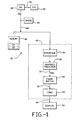
- a CPU 32 is connected to a floating point processor (FPU) 34 by bus 36.
- the CPU 32 is connected by a 32-bit system bus 38 to a random access memory (RAM) 40, a cache 42 and an interface 44 in graphics subsystem 45.
- the interface 44 is connected by bus 46 to graphics processor 48.
- the graphics processor 48 is connected by 120-bit graphics bus 50 to frame buffer 52.
- the frame buffer 52 are connected to a video digital to analog converter (DAC) 54 by bus 56.
- the DAC 54 is connected to video display 58 by line 60.
- the graphics subsystem 45 is an I/O device, and atomic access to it is required.
- Command packet interface 44 to the graphics subsystem 45 transfers geometry and graphics context information from main memory 40 to the graphics subsystem 45. For such transfers, an application writes a list of commands to a physically contiguous locked-down memory buffer 47 in its own address space. Since the system 30 has DMA, the buffer 47 resides in the main memory system 40. The system 30 has a write-back cache 42, so it moves the contents of the buffer 47 into cache 42, generating little or no traffic on bus 38 when writing to the buffer. On systems with no DMA, this buffer will reside locally on the graphics subsystem.
- the CPU 32 tells the graphics subsystem 45, via a read from an I/O address on the graphics subsystem 45, that it should begin a transfer of the command packet. Status of the operation is returned as a result of the I/O read transaction.
- the graphics subsystem 45 parses the packet and executes the appropriate operations, finding the details of the transaction syntax encoded in the first longword of the command packet. Execution of the commands in the packet is atomic, implying that all commands in one packet are executed before any commands in the next packet. Furthermore, the execution order is guaranteed to be the order in which the commands appear in the packet.
- Table 1 below shows the outline of a procedure that issues a command to draw a line in the frame buffer 52.
- the global variable, pPacket is the virtual addresses of a physically contiguous locked-down memory buffer serving as the graphics subsystem 45 command buffer 47. To avoid synchronization problems concerning the command packet memory, two command packet buffers 47 are used alternately. The alternation of command packets is handled by the switchPacket() routine.
- the Line procedure must first fill in the command packet with header information and vertex data. It then does a read from the I/O address, stamp , and receives status over the system bus 38. Table II enumerates the status values that can be returned by the graphics subsystem 45 as a result of the I/O read. Table II Value Status Description 0 GOOD Data was accepted 1 BUSY Subsystem 45 is unavailable; retry later As rectangular clipping is done in hardware, the line is clipped successively to each clipping rectangle in the window's clip list. The clip rectangle is placed in the command packet by the fillLinePacket() routine.
- the Line procedure checks the status of the I/O read transaction. If the status is GOOD, then the graphics subsystem 45 immediately initiates the transfer of the command packet. A BUSY status causes a software retry, since the procedure just spins on the status word. Neither the code of Table I nor the procedural interface of Table II is appropriate for high performance graphics. They are shown to give a trivial example of the framework of the command packet interface.
- the command packet interface provides atomic access for high level commands, such as drawing lines and triangles. Access to the graphics subsystem 45 is gained through the framework described above. In order to guarantee an atomic operation containing both the I/O read transaction issued by the application and the command packet transactions issued by the graphics subsystem 45, the physical address of the command packet is encoded in the address of the I/O read transaction. This encoding provides the packet address to the graphics subsystem 45 so that it can carry out the command packet transfer, while the application receives status as part of the same atomic operation.
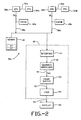
- Figure 2 shows a multiprocessor form of a system 30a, in which a first CPU 32a is connected to a FPU 34a by bus 36a.
- a cache 42a is connected to the CPU 32a by bus 38a.
- a second CPU 32b is connected to a FPU 34b by bus 36b.
- a cache 42b is connected to the CPU 32b by bus 38a.
- the construction and operation of the Figure 2 embodiment of the invention is the same as in the Figure 1 embodiment.
- bits 21:2 of the I/O read transaction address 70 contain bits 30:11 of the command packet address 72.
- the positions specified are for a 32-bit system bus 38. If the available physical address space is less than 32 bits, then the high order bits are ignored.
- the remaining bits of the address of the I/O read transaction contain an implementation specific base address that is decoded by the graphics subsystem 45, indicating that a packet transfer should be initiated.
- the address of the command packet is created as follows: bits 10:0 of the command packet address 72 are zero, forcing the packet to be aligned on a 2048 byte boundary; bits 30:11 equal bits 21:2 of the I/O read transaction address 70; bit 31 of the command packet address is zero.
- Figure 2 shows the mapping from the address 70 of the I/O read transaction to the base address 72 of the command packet transfer.
Landscapes
- Engineering & Computer Science (AREA)
- Theoretical Computer Science (AREA)
- Computer Hardware Design (AREA)
- Physics & Mathematics (AREA)
- General Engineering & Computer Science (AREA)
- General Physics & Mathematics (AREA)
- Software Systems (AREA)
- Human Computer Interaction (AREA)
- Bus Control (AREA)
- Multi Processors (AREA)
- Memory System Of A Hierarchy Structure (AREA)
Applications Claiming Priority (2)
| Application Number | Priority Date | Filing Date | Title |
|---|---|---|---|
| US440588 | 1989-11-17 | ||
| US07/440,588 US5218678A (en) | 1989-11-17 | 1989-11-17 | System and method for atomic access to an input/output device with direct memory access |
Publications (3)
| Publication Number | Publication Date |
|---|---|
| EP0430500A2 true EP0430500A2 (de) | 1991-06-05 |
| EP0430500A3 EP0430500A3 (en) | 1992-03-04 |
| EP0430500B1 EP0430500B1 (de) | 1996-09-11 |
Family
ID=23749363
Family Applications (1)
| Application Number | Title | Priority Date | Filing Date |
|---|---|---|---|
| EP90312471A Expired - Lifetime EP0430500B1 (de) | 1989-11-17 | 1990-11-15 | System und atomistische Zugriffmethode zu einer Eingaben-/Ausgabenvorrichtung mit einem direkten Speicherzugriff |
Country Status (5)
| Country | Link |
|---|---|
| US (1) | US5218678A (de) |
| EP (1) | EP0430500B1 (de) |
| JP (1) | JPH03212753A (de) |
| CA (1) | CA2030021A1 (de) |
| DE (1) | DE69028492T2 (de) |
Cited By (2)
| Publication number | Priority date | Publication date | Assignee | Title |
|---|---|---|---|---|
| WO2000010128A1 (en) * | 1998-08-10 | 2000-02-24 | Diamond Multimedia Systems, Inc. | Graphic request management system |
| SG81184A1 (en) * | 1993-12-20 | 2001-06-19 | At & T Corp | Application-oriented telecommunication system interface |
Families Citing this family (7)
| Publication number | Priority date | Publication date | Assignee | Title |
|---|---|---|---|---|
| US5666509A (en) * | 1994-03-24 | 1997-09-09 | Motorola, Inc. | Data processing system for performing either a precise memory access or an imprecise memory access based upon a logical address value and method thereof |
| US5835742A (en) * | 1994-06-14 | 1998-11-10 | Apple Computer, Inc. | System and method for executing indivisible memory operations in multiple processor computer systems with multiple busses |
| US5548780A (en) * | 1994-07-21 | 1996-08-20 | Apple Computer, Inc. | Method for semaphore communication between incompatible bus locking architectures |
| JP3209140B2 (ja) | 1997-04-04 | 2001-09-17 | 株式会社セガ | 画像処理装置 |
| US6128674A (en) * | 1997-08-08 | 2000-10-03 | International Business Machines Corporation | Method of minimizing host CPU utilization in driving an adapter by residing in system memory a command/status block a soft interrupt block and a status block queue |
| US6430628B1 (en) * | 1998-12-08 | 2002-08-06 | Intel Corporation | Method and apparatus for reducing direct memory access transfers using smart coalescing |
| US7752340B1 (en) * | 2006-03-31 | 2010-07-06 | Emc Corporation | Atomic command retry in a data storage system |
Family Cites Families (14)
| Publication number | Priority date | Publication date | Assignee | Title |
|---|---|---|---|---|
| US4402046A (en) * | 1978-12-21 | 1983-08-30 | Intel Corporation | Interprocessor communication system |
| US4491916A (en) * | 1979-11-05 | 1985-01-01 | Litton Resources Systems, Inc. | Large volume, high speed data processor |
| US4449182A (en) * | 1981-10-05 | 1984-05-15 | Digital Equipment Corporation | Interface between a pair of processors, such as host and peripheral-controlling processors in data processing systems |
| US4777595A (en) * | 1982-05-07 | 1988-10-11 | Digital Equipment Corporation | Apparatus for transferring blocks of information from one node to a second node in a computer network |
| US4689739A (en) * | 1983-03-28 | 1987-08-25 | Xerox Corporation | Method for providing priority interrupts in an electrophotographic machine |
| US4814977A (en) * | 1983-10-18 | 1989-03-21 | S&C Electric Company | Apparatus and method for direct memory to peripheral and peripheral to memory data transfers |
| US4604694A (en) * | 1983-12-14 | 1986-08-05 | International Business Machines Corporation | Shared and exclusive access control |
| JPS61107456A (ja) * | 1984-10-30 | 1986-05-26 | Toshiba Corp | 割込制御方式 |
| US4719621A (en) * | 1985-07-15 | 1988-01-12 | Raytheon Company | Packet fastbus |
| US4847754A (en) * | 1985-10-15 | 1989-07-11 | International Business Machines Corporation | Extended atomic operations |
| US5014186A (en) * | 1986-08-01 | 1991-05-07 | International Business Machines Corporation | Data-processing system having a packet transfer type input/output system |
| US4953101A (en) * | 1987-11-24 | 1990-08-28 | Digital Equipment Corporation | Software configurable memory architecture for data processing system having graphics capability |
| DE68924992T2 (de) * | 1988-02-23 | 1996-07-25 | Digital Equipment Corp | Symmetrische Steuerungsanordnung für Multiverarbeitung. |
| US5175837A (en) * | 1989-02-03 | 1992-12-29 | Digital Equipment Corporation | Synchronizing and processing of memory access operations in multiprocessor systems using a directory of lock bits |
-
1989
- 1989-11-17 US US07/440,588 patent/US5218678A/en not_active Expired - Lifetime
-
1990
- 1990-11-15 DE DE69028492T patent/DE69028492T2/de not_active Expired - Lifetime
- 1990-11-15 EP EP90312471A patent/EP0430500B1/de not_active Expired - Lifetime
- 1990-11-15 CA CA002030021A patent/CA2030021A1/en not_active Abandoned
- 1990-11-16 JP JP2311224A patent/JPH03212753A/ja active Pending
Cited By (2)
| Publication number | Priority date | Publication date | Assignee | Title |
|---|---|---|---|---|
| SG81184A1 (en) * | 1993-12-20 | 2001-06-19 | At & T Corp | Application-oriented telecommunication system interface |
| WO2000010128A1 (en) * | 1998-08-10 | 2000-02-24 | Diamond Multimedia Systems, Inc. | Graphic request management system |
Also Published As
| Publication number | Publication date |
|---|---|
| CA2030021A1 (en) | 1991-05-18 |
| DE69028492D1 (de) | 1996-10-17 |
| EP0430500A3 (en) | 1992-03-04 |
| DE69028492T2 (de) | 1997-04-03 |
| US5218678A (en) | 1993-06-08 |
| EP0430500B1 (de) | 1996-09-11 |
| JPH03212753A (ja) | 1991-09-18 |
Similar Documents
| Publication | Publication Date | Title |
|---|---|---|
| US5404522A (en) | System for constructing a partitioned queue of DMA data transfer requests for movements of data between a host processor and a digital signal processor | |
| US6023738A (en) | Method and apparatus for accelerating the transfer of graphical images | |
| US5740406A (en) | Method and apparatus for providing fifo buffer input to an input/output device used in a computer system | |
| US6046752A (en) | Peer-to-peer parallel processing graphics accelerator | |
| US5638535A (en) | Method and apparatus for providing flow control with lying for input/output operations in a computer system | |
| CA2190673C (en) | Parallel processing method for use with graphics processor | |
| JPH04233653A (ja) | 速度差が大きい協同プロセッサ間のメッセージ・キュー処理 | |
| US5805930A (en) | System for FIFO informing the availability of stages to store commands which include data and virtual address sent directly from application programs | |
| US5924126A (en) | Method and apparatus for providing address translations for input/output operations in a computer system | |
| JP2774862B2 (ja) | Dma制御装置および情報処理装置 | |
| US5396597A (en) | System for transferring data between processors via dual buffers within system memory with first and second processors accessing system memory directly and indirectly | |
| JPH07105126A (ja) | インターフェース・システムおよび方法 | |
| EP0430500B1 (de) | System und atomistische Zugriffmethode zu einer Eingaben-/Ausgabenvorrichtung mit einem direkten Speicherzugriff | |
| WO2000000887A9 (en) | Method and apparatus for transporting information to a graphic accelerator card | |
| US5887190A (en) | System for determining from a command storing in a storage circuit an application program which has initiated the command to determine an input/output device address | |
| US5764861A (en) | Apparatus and method for controlling context of input/output devices in a computer system | |
| US5129065A (en) | Apparatus and methods for interface register handshake for controlling devices | |
| US5685011A (en) | Apparatus for handling failures to provide a safe address translation in an improved input/output architecture for a computer system | |
| US6201547B1 (en) | Method and apparatus for sequencing texture updates in a video graphics system | |
| CN119645903A (zh) | 一种提高实时图像数据输入处理和输出效率的优化方法 | |
| US6677954B1 (en) | Graphics request buffer caching method | |
| US6778178B1 (en) | Memory range access flags for performance optimization | |
| JPS59112479A (ja) | キヤツシユメモリの高速アクセス方式 | |
| JPS6255693A (ja) | グラフイツクデイスプレイ装置 | |
| JPH03241442A (ja) | ストアバッファ制御方式 |
Legal Events
| Date | Code | Title | Description |
|---|---|---|---|
| PUAI | Public reference made under article 153(3) epc to a published international application that has entered the european phase |
Free format text: ORIGINAL CODE: 0009012 |
|
| 17P | Request for examination filed |
Effective date: 19901130 |
|
| AK | Designated contracting states |
Kind code of ref document: A2 Designated state(s): DE FR GB |
|
| PUAL | Search report despatched |
Free format text: ORIGINAL CODE: 0009013 |
|
| AK | Designated contracting states |
Kind code of ref document: A3 Designated state(s): DE FR GB |
|
| 17Q | First examination report despatched |
Effective date: 19940912 |
|
| GRAH | Despatch of communication of intention to grant a patent |
Free format text: ORIGINAL CODE: EPIDOS IGRA |
|
| GRAH | Despatch of communication of intention to grant a patent |
Free format text: ORIGINAL CODE: EPIDOS IGRA |
|
| GRAA | (expected) grant |
Free format text: ORIGINAL CODE: 0009210 |
|
| AK | Designated contracting states |
Kind code of ref document: B1 Designated state(s): DE FR GB |
|
| REF | Corresponds to: |
Ref document number: 69028492 Country of ref document: DE Date of ref document: 19961017 |
|
| ET | Fr: translation filed | ||
| PLBE | No opposition filed within time limit |
Free format text: ORIGINAL CODE: 0009261 |
|
| STAA | Information on the status of an ep patent application or granted ep patent |
Free format text: STATUS: NO OPPOSITION FILED WITHIN TIME LIMIT |
|
| 26N | No opposition filed | ||
| REG | Reference to a national code |
Ref country code: GB Ref legal event code: 732E |
|
| REG | Reference to a national code |
Ref country code: GB Ref legal event code: IF02 |
|
| PGFP | Annual fee paid to national office [announced via postgrant information from national office to epo] |
Ref country code: GB Payment date: 20071128 Year of fee payment: 18 Ref country code: FR Payment date: 20071119 Year of fee payment: 18 |
|
| GBPC | Gb: european patent ceased through non-payment of renewal fee |
Effective date: 20081115 |
|
| REG | Reference to a national code |
Ref country code: FR Ref legal event code: ST Effective date: 20090731 |
|
| PG25 | Lapsed in a contracting state [announced via postgrant information from national office to epo] |
Ref country code: GB Free format text: LAPSE BECAUSE OF NON-PAYMENT OF DUE FEES Effective date: 20081115 |
|
| PGFP | Annual fee paid to national office [announced via postgrant information from national office to epo] |
Ref country code: DE Payment date: 20091127 Year of fee payment: 20 |
|
| PG25 | Lapsed in a contracting state [announced via postgrant information from national office to epo] |
Ref country code: FR Free format text: LAPSE BECAUSE OF NON-PAYMENT OF DUE FEES Effective date: 20081130 |
|
| PG25 | Lapsed in a contracting state [announced via postgrant information from national office to epo] |
Ref country code: DE Free format text: LAPSE BECAUSE OF EXPIRATION OF PROTECTION Effective date: 20101115 |