EP0432076A2 - Hochleistungsschnittstelle für anteilig genutzten Hauptspeicher - Google Patents
Hochleistungsschnittstelle für anteilig genutzten Hauptspeicher Download PDFInfo
- Publication number
- EP0432076A2 EP0432076A2 EP90480175A EP90480175A EP0432076A2 EP 0432076 A2 EP0432076 A2 EP 0432076A2 EP 90480175 A EP90480175 A EP 90480175A EP 90480175 A EP90480175 A EP 90480175A EP 0432076 A2 EP0432076 A2 EP 0432076A2
- Authority
- EP
- European Patent Office
- Prior art keywords
- devices
- data bus
- master
- slave device
- data
- Prior art date
- Legal status (The legal status is an assumption and is not a legal conclusion. Google has not performed a legal analysis and makes no representation as to the accuracy of the status listed.)
- Granted
Links
Images


Classifications
-
- G—PHYSICS
- G06—COMPUTING OR CALCULATING; COUNTING
- G06F—ELECTRIC DIGITAL DATA PROCESSING
- G06F15/00—Digital computers in general; Data processing equipment in general
- G06F15/16—Combinations of two or more digital computers each having at least an arithmetic unit, a program unit and a register, e.g. for a simultaneous processing of several programs
- G06F15/163—Interprocessor communication
- G06F15/17—Interprocessor communication using an input/output type connection, e.g. channel, I/O port
-
- G—PHYSICS
- G06—COMPUTING OR CALCULATING; COUNTING
- G06F—ELECTRIC DIGITAL DATA PROCESSING
- G06F13/00—Interconnection of, or transfer of information or other signals between, memories, input/output devices or central processing units
- G06F13/14—Handling requests for interconnection or transfer
- G06F13/36—Handling requests for interconnection or transfer for access to common bus or bus system
- G06F13/368—Handling requests for interconnection or transfer for access to common bus or bus system with decentralised access control
Definitions
- the present invention relates to information processing systems in which a plurality of processing devices and memory devices share a common data bus, and more particularly to arrangements for distributing control of the data bus among the devices sharing it.
- the invention is particularly well suited for use with "smart" interfaces used by a processor sending a data request (including command and address information) to one of multiple memory cards of main storage, after which the requesting processor waits for a return of data.
- U.S-A No. 4.375.639 discloses a synchronous bus arbitration arrangement in which a communication bus includes a data bus portion including parallel data bus lines, an address bus portion and a control bus portion.
- U.S-A No. 4.561.051 discloses a memory bus with separate data, address and command paths shared by a number of independent processors.
- the data bus of the smart interface typically is scheduled for use and then remains "busy" for the entire data transfer.
- the interface is thus tied up during a relatively long memory array access time, which creates a system bottleneck when multiple processors share the interface.
- Another object of the invention is to provide a means for distributing control of a shared data bus among multiple processors and memory devices sharing the bus, while one of the devices controls the bus, to enable immediate transfer of control from the currently controlling device.
- Another object of the invention is to provide an interface between multiple processing devices and multiple memory devices in which interface overhead (i.e. the control, status and address information as opposed to the working information) is hidden from the stream of working information.
- interface overhead i.e. the control, status and address information as opposed to the working information
- Yet another object is to provide an interface between a set of processing devices configured as master devices, and a set of memory devices configured as slave devices, in which data bus control logic among all devices is employed in combination with arbitration logic for determining priority among only the master devices, and in which the function of memory array address generation resides in the memory devices.
- an information processing system including a plurality of devices for transmitting and receiving bit-encoded working information.
- the system comprises a first set of devices including at least one master device, a second set of devices including at least one slave device, and an interface between the first and second sets of devices.
- the interface includes a first data bus shared by the devices for carrying out transmissions of the working information between the first and second set of devices.
- Each of the devices when providing working information to the first data bus during one of the transmissions, exclusively controls the first data bus.
- the interface further includes a bidirectional signal conveyance means connected to the first and second sets of devices, for transmitting a data bus hold signal from one of the devices currently in control of the first data bus to the other devices, to prevent another device from controlling the first data bus until the currently controlling device has completed one of the transmissions.
- the interface includes a selection means connected to the first and second sets of devices. The selection means permits transmissions of control signals, each from a selected one of the master devices to a selected one of the slave devices, thereby to allow transfer of control of the first data bus to one of the devices after the currently controlling device completes its transmission.
- the control signals include a first control signal, operative after termination of the data bus hold signal, to transfer control of the first data bus, enabling the selected master device to transmit working information to a selected slave device over the first data bus; a second control signal to enable a selected slave device to buffer working information for its subsequent transmission from a selected slave device to a selected master device; and a third control signal, operative after termination of the data bus hold signal, to pass control of the first data bus to the selected slave device via the selected master device for transmission of the previously buffered working information to the selected master device.
- the first set of devices includes a plurality of master devices, several of which are processors, while the second set of devices includes a plurality of slave devices, several of which are memory cards.
- the network preferably includes an arbitration scheme, operative only among the master devices, for determining priority of generating control signal, i.e. priority of access to the first data bus.
- the present invention is not an arbitration scheme, but rather suited for use in combination with an arbitration scheme to more effectively employ a shared data bus. Accordingly, the arbitration scheme can involve arbitration logic within each master device, or a single arbiter connected to all of the master devices, in either case according to practices known in the art.
- the network advantageously employs a second data bus for transmitting command and address information, and a third data bus for transmitting command received acknowledgements and other status information.
- the busses are connected to all of the devices, and operate in parallel.
- the data bus hold signal is conveyed by a single line grant token connected to all of the devices, and the selection means includes a plurality of select tokens.
- Each of the select tokens consists of a command active line for transmitting the first and second control signals, a return data line for transmitting the third control signal, and a buffer-full line for transmitting, from its associated slave device to all master devices, an indication that its buffer is occupied.
- each select token is connected only to its associated slave device and to all of the master devices.
- transfer of control among devices follows protocols associated with two types of commands: a storage command for the transfer of working information from a master device to a slave device, and a fetch command for transfer of data from a slave device to a master device.
- a storage command for the transfer of working information from a master device to a slave device
- a fetch command for transfer of data from a slave device to a master device.
- a fetch operation involves three stages: an initial stage in which a fetch command is provided from a selected master to a selected slave over the second data bus and simultaneously the first control signal is provided to the selective slave device.
- the slave device accesses it memory arrays for the requested data.
- the slave device controls the first data bus to send the requested working information to the master device.
- Each memory card includes sufficient logic for processing access requests independently of processor control, thus freeing the first data bus, during the second stage of the fetch operation, to handle data unrelated to the fetch operation.
- An information processing network offers a number of features contributing to high efficiency of the shared interface.
- the grant and select tokens distribute control of the working data bus among all of the devices, and transfer control of this bus prior to its use.
- Certain simple data manipulation operations, including memory array address generation are shifted from the processors to the memory cards. This requires a high level command set to control the memory cards, but reduces the burden on the interface.
- the separate command/address bus permits parallel transmission of commands and working data between two unique pairs of devices.
- the above features facilitate use of the working data bus at nearly 100 percent for maximum interface efficiency. They promote flexibility, in that slave devices of different types can be employed in the same network. A slave device operating at a slower rate simply holds the interface longer when return of data is requested. The only necessary conditions for the interface are that all memory cards must have the same synchronized cycle time and use compatible technologies for the bus logic, i.e. the drivers and receivers.
- the dual-token passing scheme substantially enhances the effectiveness of the interface in handling multiple processors and I/O devices sharing a single data path to main storage, thus substantially increasing total system performance.
- FIG. 1 is a schematic illustration of an information processing network configured in accordance with the present invention
- Figure 2 is a more detailed schematic of the network illustrating features of an interface between master devices and slave devices;
- Figure 3 is a timing diagram showing the protocol of the interface for data storage transfers
- Figure 4 is a timing diagram illustrating the protocol of the interface for return data transfers
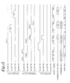
- Figure 5 is a timing diagram illustrating a sequence of storage and data fetch operations according to the interface protocols
- Figure 6 is a timing diagram illustrating a sequence similar to that of Figure 5, but including the acknowledgement feature of the protocol illustrated in Figure 3;
- Figure 7 is a timing diagram showing a sequence similar to that of Figure 5, but with a memory card of the network occupied.
- the master set includes a plurality of main processors 20.
- the set of slave devices includes main storage, including a plurality of memory cards 22.
- the slave devices further include an auxiliary slave device 24, which can be, for example, an I/0 device, a vector processor, an auxiliary processor, etc.
- Networks such as a network 16 may include a plurality of auxiliary slave devices, or alternatively no such devices. In any event the network includes at least one master device and at least one slave device.
- Network 16 is shown in more detail in Figure 2.
- the master set includes "N" processors, with the first and second processors shown at 26 and 28, respectively.
- Processor 26 includes arbitration logic 30, and processor 28 includes substantially identical arbitration logic 32.
- the remaining processors likewise include the arbitration logic.
- Each of the processors is connected to all of the remaining processors in point-to-point fashion, i.e. by multiple lines. A set of such lines links the arbitration logic circuitry in each processor with the corresponding circuitry in each of the other processors. These lines are labeled 2-N for the first processor and 1 and 3-N in the second processor.
- Each of the processors further includes interface control logic for use in distributing control of interface 18 among the processors and slave devices, as indicated at 34 and 36 in connection with processors 26 and 28, respectively.
- Slave device 38 includes interface control logic circuitry 46, with slave devices 40-44 including substantially identical interface control logic circuitry at 48, 50 and 52.
- Slave device 38 further includes memory arrays, indicated at 54, for storing bit-encoded data, and a buffer 56 for intermediate storage of working data received from interface 18, and for loading data retrieved from the arrays for transmission. Similar memory arrays 58, 60 and 62 and buffers 64, 66 and 68 are part of slave devices 40, 42 and 44, respectively.
- Interface 18 is shared in common by all of the master devices and all of the slave devices, for transmitting working information between individual master and slave devices, typically for manipulation within a master device or storage within a slave device.
- the interface further accommodates transmissions of control, address and status information, all of which concern the handling of the working information.
- Interface 18 includes three busses for data transmissions, including a data bus 70 for transmitting working information, a command/address bus 72 for transmitting store and fetch commands, address information and the number of data bytes involved, and a communication bus 74 for transmitting status information.
- Interface 18 further includes a series of lines for passing control of the interface among the master devices and slave devices. These include a grant token 76, which is a single line shared in common by all devices, and a series of "X" select tokens, each uniquely associated with one of the slave devices and connected to all of the master devices.
- the select token connected to slave device 38 is shown in detail to reveal that it consists of three lines: a command active line 78, a return data line 80 and a buffer full or buffer occupied line 82.
- the interface lines making up the select tokens transmit data bus control signals between the master devices and slave devices, for passing control of data bus 70 among these devices.
- Grant token 76 is a single line connected to each of the master and slave devices for bidirectional transmission. In other words, each of the master and slave devices can either drive the grant token, or receive signals from the grant token.
- a device When a device is sending working information to another one of the devices over data bus 70, it controls the data bus to the exclusion of all other devices.
- This device for convenience designated the “currently controlling” device, maintains control of bus 70 by providing a data bus hold signal via grant token 76 to the other devices. More particularly, grant token 76 must be active in order to permit the select tokens to shift data bus control to one of the other devices.
- the currently controlling device maintains control by deactivating, and maintaining inactive, the grant token.
- this device activates the grant token. This is done e.g. by changing the logic level of the signal to the grant token from a "0" to "1".
- Activation of grant token 76 is a signal to all devices that the currently controlling device is on the final cycle of its operation, which frees the interface for the following cycle.
- the select tokens shift control of data bus 70 to the next one of the devices, so that the next device can provide data to data bus 70 immediately upon completion of the current transmission.
- command active line 78 for a store command transmits a "command active" signal from any of the master devices to slave device 38, signalling that a selected one of the master devices has been granted control of the data bus for the next operation.
- Return data line 80 also transmits a control signal from any of the master devices to slave device 38, in this instance indicating that control of data bus 70 is being passed from the selected master device to slave device 38 for sending data to the selected master via the data bus.
- Buffer occupied line 82 is also unidirectional, but transmits a buffer-full signal from slave device 38 to all of the master devices. This signal indicates that slave device 38, typically because buffer 56 is occupied, will not accept commands from any of the master devices, either to receive data from a master device for storage, or to retrieve data from arrays 54 into its buffer for later transmission to a selected master device.
- each command active line is driven from a selected master device to the slave device uniquely associated with the select token.
- Each return data line is likewise driven from a selected master device to a unique slave device, and instructs the slave device to send previously requested data to the selected master device on the following cycle.
- Data bus control signals provided over the command active and return data lines are of course valid only if the grant token is active. If the grant token is being held inactive by a currently controlling device, such signals are ignored and must be reissued by the selected master devices to become effective when issued with the grant token active.
- Each buffer full line is driven from its uniquely associated slave device to all of the master devices. When this line is active, the associated slave does not accept commands, regardless of the state of any of the other lines.
- Data bus 70 is bidirectional. It is the exclusive conduit for working information, and transmits only working information. All of the master devices and slave devices are connected to bus 70 for transmissions, so that each of the devices can drive bus 70 when controlling it and transmitting working information, and further can receive working information transmitted from another device. Data bus 70 preferably is able to transmit up to eight data bytes in parallel, although the capacity of this bus may be varied to suit the needs of particular networks.
- Command/address bus 72 transmits information from a selected master device to a selected slave device.
- the information includes a command (i.e. store or fetch), a byte-aligned start address at which data is located or data is to be stored, and the length of the address in terms of the number of bytes involved.
- the slave devices receive but do not send this information.
- the bidirectional connection of the master devices with bus 72 enables each master device, when providing command and address information to bus 72, to inform the other master devices as to the length and address of the access.
- Communication bus 74 is common to all master and slave devices, and functions in parallel with data bus 70 and command/address bus 72.
- the communication bus is driven from the slave devices to the master devices, and provides the communication link between the master and slave devices which adds intelligence to the interface.
- Communication bus 74 operates under three protocols to transfer information, with the current protocol determined by the data bus control signals issued on the previous cycle and the grant token of the current cycle.
- a slave device controlling data bus 70 and transmitting working information to one of the master devices, simultaneously transmits status information to that master device.
- the status information is related to the working information being simultaneously transmitted, and identifies the working information as good, bad or corrected.
- This protocol is valid if the slave device controls the interface (i.e. data bus 70) to return data and is currently activating grant token 76.
- a selected slave device notifies a master device that it needs service, i.e. is subject to internal error, trap condition, etc.
- This protocol is valid when the slave device controls interface 18 to return data, but has not activated the grant token, indicating that the slave device is not yet returning control of the interface.
- the third protocol is optional, and is used by a slave device to notify a processor or other master device either that it has received a command or has not received the command (e.g. card busy), the command having been sent by the master device during the previous clock cycle. Further under this protocol, the slave device may provide a message that service is needed. This protocol is valid during the cycle following activation of the associated command activate line and the grant token. Transfers between the master devices and slave devices are
- Store and fetch operations are conducted according to two protocols of interface 18, one for command transfers and one for return data transfers.
- the command transfer protocol is illustrated in Figure 3, and can apply either to a store operation or the initial stage of a fetch operation.
- a selected master device activates the command activate line and the grant token, and simultaneously provides a command to a selected slave device via command/address bus 72. If the command is part of a store operation, working data is sent from the master device to the slave device via data bus 70 during the next subsequent clock cycle. Further, if the optional acknowl edge protocol is used, the slave device sends an acknowledgement to the master device that the store command was received, over communication bus 74.
- a selected master device activates the return data line associated with a selected slave device, as well as grant token 76, unless the grant token is being controlled by another slave device. Control of the grant token is transferred to the slave device.
- the slave device maintains the grant token activate, transfers requested data to the master device over data bus 70, and simultaneously transfers related status information to the master device via the communication bus.
- Each storage operation involves a command transfer, with a command involved being a store command.
- Fetch operations occur in three stages.
- a fetch command is sent from the master device to the slave device under the command transfer protocol, with a difference from Figure 3 in that no data is transferred over the interface during the next subsequent clock cycle.
- the slave device responsive to the fetch command, retrieves the requested data from its memory arrays and transfers the retrieved data into its buffer.
- the previously buffered data is transmitted to the master device, responsive to activation of the associated return data line by the master device and the accompanying transfer of bus control to the slave device.
- the particular master device to issue the store command and activate the command active line is selected pursuant to an arbitration scheme not in itself germane to the present invention, but selected from a number of arbitration schemes known to those skilled in the art and used in cooperation with the present invention.
- a salient feature of the present invention is increased efficiency of the interface, principally due to more effective use of data bus 70.
- Figure 5 illustrates a series of command and return data transfers over fifteen clock cycles, in which the use of data bus 70 after the first clock cycle is 100 percent.
- the timing diagram illustrates transmissions between master devices 26 and 29, and slave devices 38, 40 42 and 44, connected to one another through the interface.
- Figure 6 illustrates a timed sequence of operations similar to those in Figure 5, but with the optional acknowledgement protocol. Accordingly, communication bus 74 transfers not only status information, but acknowledgements from the slave devices to the master devices that commands have been received. In clock cycles 2 and 3, slave devices 38 and 40 acknowledge "store command received" to master devices 26 and 28, respectively. In clock cycle 4, slave device 38 acknowledges to master device 26 its receipt of the fetch command issued in the previous cycle.
- the timing diagram in Figure 7 illustrates the situation in which one of the slave devices has been enabled to return or send data to a selected master device, but is unable to return data, perhaps because the data has not yet been retrieved from the memory card data arrays.
- actuation of the associated return data line transfers control of data bus 70 from the selected master to the selected slave, as before.
- the slave device simply maintains control of the grant token, holding the grant line inactive until the slave device can transmit the requested data.
- this sequence of events is illustrated in connection with master device 26 and slave device 38.
- the corresponding return data line is activat ed in clock cyle 6.
- Slave device 38 in control of the grant token during cycles 7-9, transmits an appropriate signal pursuant to the second of the three protocols discussed above in connection with communication bus 74.
- This protocol is valid, as slave device 38 controls data bus 70 but has not activated the grant token.
- slave device 38 activates the grant token and transfers the requested working information to master device 26 via data bus 70.
- master device 28 is unable to obtain control for transferring data to slave device 42.
- master device 28 continues to issue a store command, and maintains the associated command active line active in cycles 6-9 until slave device 38 raises the grant token to complete both the command from master 28 to salve 42 and the data transfer from slave 38 to master 26.
- multiple processors and I/O devices can share the same data bus to main storage, with total system performance substantially enhanced through effective use of the data bus.
- devices configured as masters require both arbitration and bus sharing logic
- the slave devices need only the bus sharing logic to distribute control of the data bus among all master and slave devices.
- the use of the additional command/address bus and communication bus in parallel with the data bus, with an interface protocol selection of the next interface controller during a current transmission substantially enhances use of the working data bus.
- the transfer of certain logic functions from master processors to slave memory cards, and a data fetch protocol which frees the busses for unrelated transfers during one stage of the fetch operation further enhance bus utilization.
Landscapes
- Engineering & Computer Science (AREA)
- Theoretical Computer Science (AREA)
- Computer Hardware Design (AREA)
- Physics & Mathematics (AREA)
- General Engineering & Computer Science (AREA)
- General Physics & Mathematics (AREA)
- Software Systems (AREA)
- Bus Control (AREA)
- Multi Processors (AREA)
Applications Claiming Priority (2)
| Application Number | Priority Date | Filing Date | Title |
|---|---|---|---|
| US445320 | 1989-12-04 | ||
| US07/445,320 US5131085A (en) | 1989-12-04 | 1989-12-04 | High performance shared main storage interface |
Publications (3)
| Publication Number | Publication Date |
|---|---|
| EP0432076A2 true EP0432076A2 (de) | 1991-06-12 |
| EP0432076A3 EP0432076A3 (en) | 1993-09-29 |
| EP0432076B1 EP0432076B1 (de) | 1997-01-08 |
Family
ID=23768465
Family Applications (1)
| Application Number | Title | Priority Date | Filing Date |
|---|---|---|---|
| EP90480175A Expired - Lifetime EP0432076B1 (de) | 1989-12-04 | 1990-10-31 | Hochleistungsschnittstelle für anteilig genutzten Hauptspeicher |
Country Status (4)
| Country | Link |
|---|---|
| US (1) | US5131085A (de) |
| EP (1) | EP0432076B1 (de) |
| JP (1) | JPH0619754B2 (de) |
| DE (1) | DE69029648T2 (de) |
Cited By (2)
| Publication number | Priority date | Publication date | Assignee | Title |
|---|---|---|---|---|
| EP0518527A3 (de) * | 1991-05-28 | 1993-01-07 | Hewlett-Packard Company | Verfahren zur Verminderung der Restbandbreite eines Busses in einem Rechnersystem |
| WO1995020192A1 (en) * | 1994-01-25 | 1995-07-27 | Apple Computer, Inc. | Bus deadlock avoidance during master split-transactions |
Families Citing this family (27)
| Publication number | Priority date | Publication date | Assignee | Title |
|---|---|---|---|---|
| US5276809A (en) * | 1990-06-26 | 1994-01-04 | Digital Equipment Corporation | Method and apparatus for capturing real-time data bus cycles in a data processing system |
| US5339397A (en) * | 1990-10-12 | 1994-08-16 | International Business Machines Corporation | Hardware primary directory lock |
| US5953510A (en) * | 1991-09-05 | 1999-09-14 | International Business Machines Corporation | Bidirectional data bus reservation priority controls having token logic |
| US5422885A (en) * | 1992-06-01 | 1995-06-06 | Motorola, Inc. | Contention free local area network |
| DE4317567A1 (de) * | 1993-05-26 | 1994-12-01 | Siemens Ag | Verfahren zum Betreiben eines Bussystems sowie Anordnung zur Durchführung des Verfahrens |
| US5572687A (en) * | 1994-04-22 | 1996-11-05 | The University Of British Columbia | Method and apparatus for priority arbitration among devices in a computer system |
| US5717931A (en) * | 1994-12-20 | 1998-02-10 | Motorola, Inc. | Method and apparatus for communicating between master and slave electronic devices where the slave device may be hazardous |
| US6199133B1 (en) * | 1996-03-29 | 2001-03-06 | Compaq Computer Corporation | Management communication bus for networking devices |
| US6081860A (en) * | 1997-11-20 | 2000-06-27 | International Business Machines Corporation | Address pipelining for data transfers |
| US6185646B1 (en) * | 1997-12-03 | 2001-02-06 | International Business Machines Corporation | Method and apparatus for transferring data on a synchronous multi-drop |
| WO2000017726A2 (en) * | 1998-09-18 | 2000-03-30 | Computron | Switchable master/slave memory controller |
| US6658552B1 (en) * | 1998-10-23 | 2003-12-02 | Micron Technology, Inc. | Processing system with separate general purpose execution unit and data string manipulation unit |
| US6684279B1 (en) * | 1999-11-08 | 2004-01-27 | International Business Machines Corporation | Method, apparatus, and computer program product for controlling data transfer |
| US20020178283A1 (en) * | 2001-03-29 | 2002-11-28 | Pelco, A Partnership | Real-time networking protocol |
| US7007121B1 (en) * | 2002-02-27 | 2006-02-28 | Xilinx, Inc. | Method and apparatus for synchronized buses |
| US6934782B2 (en) * | 2002-12-23 | 2005-08-23 | Lsi Logic Corporation | Process and apparatus for managing use of a peripheral bus among a plurality of controllers |
| EP2005214A4 (de) * | 2006-03-30 | 2012-04-18 | Given Imaging Ltd | In-vivo-messeinrichtung und verfahren zur kommunikation zwischen bildgebern und prozessor dafür |
| US8935336B2 (en) * | 2008-06-18 | 2015-01-13 | Cisco Technology, Inc. | Optimizing program requests over a wide area network |
| KR101611157B1 (ko) * | 2009-11-24 | 2016-04-11 | 삼성전자 주식회사 | 공기조화기 및 그 통신방법 |
| US9398080B2 (en) * | 2012-03-15 | 2016-07-19 | Omron Corporation | Control device, image processing device, control method, computer-readable recording medium, and program |
| US9698852B2 (en) * | 2012-10-30 | 2017-07-04 | Maja Systems, Inc. | Compact and low-power millimeter-wave integrated VCO-up/down-converter with gain-boosting |
| US9213660B2 (en) * | 2013-06-14 | 2015-12-15 | Arm Limited | Receiver based communication permission token allocation |
| US9665707B2 (en) * | 2015-01-09 | 2017-05-30 | GM Global Technology Operations LLC | Systems and methods for cyber security of intra-vehicular peripherals powered by wire |
| DE102017117288A1 (de) * | 2017-07-31 | 2019-01-31 | Hengstler Gmbh | Datenübertragungsverfahren zwischen einem Drehwinkelgeber und einer Motorsteuereinrichtung oder einer Auswerteeinheit |
| US11580058B1 (en) | 2021-08-30 | 2023-02-14 | International Business Machines Corporation | Hierarchical ring-based interconnection network for symmetric multiprocessors |
| US12265850B2 (en) * | 2021-08-30 | 2025-04-01 | International Business Machines Corporation | Reservation mechanism for node with token constraints for preventing node starvation in a circular topology network |
| US12405826B2 (en) | 2021-08-30 | 2025-09-02 | International Business Machines Corporation | Reservation mechanism for nodes with phase constraints |
Family Cites Families (17)
| Publication number | Priority date | Publication date | Assignee | Title |
|---|---|---|---|---|
| US4223380A (en) * | 1978-04-06 | 1980-09-16 | Ncr Corporation | Distributed multiprocessor communication system |
| FR2474199B1 (fr) * | 1980-01-21 | 1986-05-16 | Bull Sa | Dispositif pour superposer les phases successives du transfert des informations entre plusieurs unites d'un systeme de traitement de l'information |
| US4314335A (en) * | 1980-02-06 | 1982-02-02 | The Perkin-Elmer Corporation | Multilevel priority arbiter |
| US4375639A (en) * | 1981-01-12 | 1983-03-01 | Harris Corporation | Synchronous bus arbiter |
| CA1179069A (en) * | 1981-04-10 | 1984-12-04 | Yasushi Fukunaga | Data transmission apparatus for a multiprocessor system |
| US4481572A (en) * | 1981-10-13 | 1984-11-06 | Teledyne Industries, Inc. | Multiconfigural computers utilizing a time-shared bus |
| US4504906A (en) * | 1982-11-30 | 1985-03-12 | Anritsu Electric Company Limited | Multiprocessor system |
| US4698746A (en) * | 1983-05-25 | 1987-10-06 | Ramtek Corporation | Multiprocessor communication method and apparatus |
| JPS60107170A (ja) * | 1983-11-15 | 1985-06-12 | Nec Corp | マルチプロセッサ制御方式 |
| JPS60129872A (ja) * | 1983-12-19 | 1985-07-11 | Toshiba Corp | デ−タの分散処理装置 |
| US4561051A (en) * | 1984-02-10 | 1985-12-24 | Prime Computer, Inc. | Memory access method and apparatus in multiple processor systems |
| US4633394A (en) * | 1984-04-24 | 1986-12-30 | International Business Machines Corp. | Distributed arbitration for multiple processors |
| US4639859A (en) * | 1984-05-24 | 1987-01-27 | Rca Corporation | Priority arbitration logic for a multi-master bus system |
| US4719622A (en) * | 1985-03-15 | 1988-01-12 | Wang Laboratories, Inc. | System bus means for inter-processor communication |
| US4730268A (en) * | 1985-04-30 | 1988-03-08 | Texas Instruments Incorporated | Distributed bus arbitration for a multiprocessor system |
| US4803617A (en) * | 1986-02-10 | 1989-02-07 | Eastman Kodak Company | Multi-processor using shared buses |
| EP0257061A1 (de) * | 1986-02-10 | 1988-03-02 | EASTMAN KODAK COMPANY (a New Jersey corporation) | Vielfachprozessorvorrichtung |
-
1989
- 1989-12-04 US US07/445,320 patent/US5131085A/en not_active Expired - Fee Related
-
1990
- 1990-10-31 DE DE69029648T patent/DE69029648T2/de not_active Expired - Fee Related
- 1990-10-31 EP EP90480175A patent/EP0432076B1/de not_active Expired - Lifetime
- 1990-11-26 JP JP2318196A patent/JPH0619754B2/ja not_active Expired - Lifetime
Cited By (3)
| Publication number | Priority date | Publication date | Assignee | Title |
|---|---|---|---|---|
| EP0518527A3 (de) * | 1991-05-28 | 1993-01-07 | Hewlett-Packard Company | Verfahren zur Verminderung der Restbandbreite eines Busses in einem Rechnersystem |
| WO1995020192A1 (en) * | 1994-01-25 | 1995-07-27 | Apple Computer, Inc. | Bus deadlock avoidance during master split-transactions |
| US5469435A (en) * | 1994-01-25 | 1995-11-21 | Apple Computer, Inc. | Bus deadlock avoidance during master split-transactions |
Also Published As
| Publication number | Publication date |
|---|---|
| US5131085A (en) | 1992-07-14 |
| EP0432076A3 (en) | 1993-09-29 |
| JPH0619754B2 (ja) | 1994-03-16 |
| DE69029648T2 (de) | 1997-07-17 |
| EP0432076B1 (de) | 1997-01-08 |
| JPH03214343A (ja) | 1991-09-19 |
| DE69029648D1 (de) | 1997-02-20 |
Similar Documents
| Publication | Publication Date | Title |
|---|---|---|
| EP0432076B1 (de) | Hochleistungsschnittstelle für anteilig genutzten Hauptspeicher | |
| EP0391583B1 (de) | Zweiweg-Rechnerverbindungssystem mit Steuerung eines Paketspeichers mit vier Anschlussstellen | |
| US5020020A (en) | Computer interconnect system with transmit-abort function | |
| US5187780A (en) | Dual-path computer interconnect system with zone manager for packet memory | |
| US5948060A (en) | Speeding-up communication rates on links transferring data structures by a method of handing scatter/gather of storage blocks in commanded computer systems | |
| US5604866A (en) | Flow control system having a counter in transmitter for decrementing and incrementing based upon transmitting and received message size respectively for indicating free space in receiver | |
| US5828899A (en) | System for peripheral devices recursively generating unique addresses based on the number of devices connected dependent upon the relative position to the port | |
| US5175732A (en) | Method and apparatus for controlling data communication operations within stations of a local-area network | |
| EP0993680B1 (de) | Verfahren und vorrichtung in einem paketenleitweglenkungsschalter um den zugriff zu einem gemeinsamen speicher auf verschiedenen datenraten zu steuern | |
| EP0991999B1 (de) | Verfahren und vorrichtung zur zugriffsarbitrierung auf einen gemeinsamen speicher von mit unterschiedlichen geschwindigkeiten arbeitenden netzwerkanschlussstellen | |
| EP0674276B1 (de) | Ein Rechnersystem | |
| US5781741A (en) | Message communications system in a parallel computer | |
| US20090024776A1 (en) | High data rate serial peripheral interface | |
| US20020133646A1 (en) | Method and device for providing high data rate for a serial peripheral interface | |
| WO1991020045A1 (en) | Distributed architecture for input/output for a multiprocessor system | |
| EP1302050A1 (de) | Kommunikationssteuerungsverfahren und einheit | |
| US20040230717A1 (en) | Processing device | |
| JP4104939B2 (ja) | マルチプロセッサシステム | |
| US5970253A (en) | Priority logic for selecting and stacking data | |
| US4959843A (en) | Content induced transaction overlap (CITO) block transmitter | |
| JP2000244585A (ja) | バスインタフェース回路 | |
| JPH0766361B2 (ja) | データ転送方法 | |
| JP2666782B2 (ja) | 多重バス制御システム | |
| JP3457084B2 (ja) | パケットバス制御装置 | |
| IE901711A1 (en) | Dual-path computer interconnect system with four-ported¹packet memory control |
Legal Events
| Date | Code | Title | Description |
|---|---|---|---|
| PUAI | Public reference made under article 153(3) epc to a published international application that has entered the european phase |
Free format text: ORIGINAL CODE: 0009012 |
|
| 17P | Request for examination filed |
Effective date: 19901213 |
|
| AK | Designated contracting states |
Kind code of ref document: A2 Designated state(s): DE FR GB IT |
|
| PUAL | Search report despatched |
Free format text: ORIGINAL CODE: 0009013 |
|
| AK | Designated contracting states |
Kind code of ref document: A3 Designated state(s): DE FR GB IT |
|
| GRAG | Despatch of communication of intention to grant |
Free format text: ORIGINAL CODE: EPIDOS AGRA |
|
| 17Q | First examination report despatched |
Effective date: 19960214 |
|
| GRAH | Despatch of communication of intention to grant a patent |
Free format text: ORIGINAL CODE: EPIDOS IGRA |
|
| GRAH | Despatch of communication of intention to grant a patent |
Free format text: ORIGINAL CODE: EPIDOS IGRA |
|
| GRAA | (expected) grant |
Free format text: ORIGINAL CODE: 0009210 |
|
| AK | Designated contracting states |
Kind code of ref document: B1 Designated state(s): DE FR GB IT |
|
| PG25 | Lapsed in a contracting state [announced via postgrant information from national office to epo] |
Ref country code: FR Free format text: THE PATENT HAS BEEN ANNULLED BY A DECISION OF A NATIONAL AUTHORITY Effective date: 19970108 |
|
| REF | Corresponds to: |
Ref document number: 69029648 Country of ref document: DE Date of ref document: 19970220 |
|
| ITF | It: translation for a ep patent filed | ||
| ET | Fr: translation filed | ||
| PLBE | No opposition filed within time limit |
Free format text: ORIGINAL CODE: 0009261 |
|
| STAA | Information on the status of an ep patent application or granted ep patent |
Free format text: STATUS: NO OPPOSITION FILED WITHIN TIME LIMIT |
|
| 26N | No opposition filed | ||
| PG25 | Lapsed in a contracting state [announced via postgrant information from national office to epo] |
Ref country code: DE Free format text: LAPSE BECAUSE OF NON-PAYMENT OF DUE FEES Effective date: 19980701 |
|
| REG | Reference to a national code |
Ref country code: FR Ref legal event code: ST |
|
| PGFP | Annual fee paid to national office [announced via postgrant information from national office to epo] |
Ref country code: GB Payment date: 19990930 Year of fee payment: 10 |
|
| PG25 | Lapsed in a contracting state [announced via postgrant information from national office to epo] |
Ref country code: GB Free format text: LAPSE BECAUSE OF NON-PAYMENT OF DUE FEES Effective date: 20001031 |
|
| GBPC | Gb: european patent ceased through non-payment of renewal fee |
Effective date: 20001031 |
|
| PG25 | Lapsed in a contracting state [announced via postgrant information from national office to epo] |
Ref country code: IT Free format text: LAPSE BECAUSE OF NON-PAYMENT OF DUE FEES Effective date: 20051031 |