EP0432481A2 - Procédés et appareil de vérification de l'état d'une pluralité de cellules de mémoires électriquement programmables - Google Patents
Procédés et appareil de vérification de l'état d'une pluralité de cellules de mémoires électriquement programmables Download PDFInfo
- Publication number
- EP0432481A2 EP0432481A2 EP90121675A EP90121675A EP0432481A2 EP 0432481 A2 EP0432481 A2 EP 0432481A2 EP 90121675 A EP90121675 A EP 90121675A EP 90121675 A EP90121675 A EP 90121675A EP 0432481 A2 EP0432481 A2 EP 0432481A2
- Authority
- EP
- European Patent Office
- Prior art keywords
- source
- array
- sensing
- voltage
- circuitry
- Prior art date
- Legal status (The legal status is an assumption and is not a legal conclusion. Google has not performed a legal analysis and makes no representation as to the accuracy of the status listed.)
- Withdrawn
Links
- 238000000034 method Methods 0.000 title claims description 15
- 230000004044 response Effects 0.000 claims abstract description 13
- 230000005669 field effect Effects 0.000 claims description 37
- 238000009877 rendering Methods 0.000 claims description 3
- 230000008878 coupling Effects 0.000 claims 16
- 238000010168 coupling process Methods 0.000 claims 16
- 238000005859 coupling reaction Methods 0.000 claims 16
- 238000010586 diagram Methods 0.000 description 14
- 230000035945 sensitivity Effects 0.000 description 8
- 238000003491 array Methods 0.000 description 5
- 230000006870 function Effects 0.000 description 5
- 230000002093 peripheral effect Effects 0.000 description 3
- 238000012795 verification Methods 0.000 description 3
- 230000000295 complement effect Effects 0.000 description 1
- 230000004069 differentiation Effects 0.000 description 1
- 239000012634 fragment Substances 0.000 description 1
- 230000007274 generation of a signal involved in cell-cell signaling Effects 0.000 description 1
- 238000004519 manufacturing process Methods 0.000 description 1
- KJLLKLRVCJAFRY-UHFFFAOYSA-N mebutizide Chemical compound ClC1=C(S(N)(=O)=O)C=C2S(=O)(=O)NC(C(C)C(C)CC)NC2=C1 KJLLKLRVCJAFRY-UHFFFAOYSA-N 0.000 description 1
- 229910044991 metal oxide Inorganic materials 0.000 description 1
- 150000004706 metal oxides Chemical class 0.000 description 1
- 230000008569 process Effects 0.000 description 1
- 239000004065 semiconductor Substances 0.000 description 1
Images


Classifications
-
- G—PHYSICS
- G11—INFORMATION STORAGE
- G11C—STATIC STORES
- G11C16/00—Erasable programmable read-only memories
- G11C16/02—Erasable programmable read-only memories electrically programmable
- G11C16/06—Auxiliary circuits, e.g. for writing into memory
- G11C16/34—Determination of programming status, e.g. threshold voltage, overprogramming or underprogramming, retention
- G11C16/3436—Arrangements for verifying correct programming or erasure
- G11C16/3454—Arrangements for verifying correct programming or for detecting overprogrammed cells
- G11C16/3459—Circuits or methods to verify correct programming of nonvolatile memory cells
-
- G—PHYSICS
- G11—INFORMATION STORAGE
- G11C—STATIC STORES
- G11C16/00—Erasable programmable read-only memories
- G11C16/02—Erasable programmable read-only memories electrically programmable
- G11C16/06—Auxiliary circuits, e.g. for writing into memory
- G11C16/10—Programming or data input circuits
-
- G—PHYSICS
- G11—INFORMATION STORAGE
- G11C—STATIC STORES
- G11C16/00—Erasable programmable read-only memories
- G11C16/02—Erasable programmable read-only memories electrically programmable
- G11C16/06—Auxiliary circuits, e.g. for writing into memory
- G11C16/34—Determination of programming status, e.g. threshold voltage, overprogramming or underprogramming, retention
- G11C16/3436—Arrangements for verifying correct programming or erasure
- G11C16/3454—Arrangements for verifying correct programming or for detecting overprogrammed cells
-
- G—PHYSICS
- G11—INFORMATION STORAGE
- G11C—STATIC STORES
- G11C29/00—Checking stores for correct operation ; Subsequent repair; Testing stores during standby or offline operation
- G11C29/04—Detection or location of defective memory elements, e.g. cell constructio details, timing of test signals
- G11C29/50—Marginal testing, e.g. race, voltage or current testing
-
- G—PHYSICS
- G11—INFORMATION STORAGE
- G11C—STATIC STORES
- G11C16/00—Erasable programmable read-only memories
- G11C16/02—Erasable programmable read-only memories electrically programmable
- G11C16/04—Erasable programmable read-only memories electrically programmable using variable threshold transistors, e.g. FAMOS
-
- G—PHYSICS
- G11—INFORMATION STORAGE
- G11C—STATIC STORES
- G11C29/00—Checking stores for correct operation ; Subsequent repair; Testing stores during standby or offline operation
- G11C29/04—Detection or location of defective memory elements, e.g. cell constructio details, timing of test signals
- G11C29/50—Marginal testing, e.g. race, voltage or current testing
- G11C2029/5004—Voltage
Definitions
- the present invention relates in general to programmable memory cells, and more particularly to methods and apparatus for verifying the state of a plurality of electrically programmable memory cells.
- EPROM electrically programmable read only memory
- an array source or decoded ground on one end of a current path of a selected memory cell is brought low.
- the bit line is connected to a voltage bias source. Since the current path of the memory cell is interposed between the bit line and the selected array source, its conductance state may be ascertained by sensing the voltage level of the bit line. If the voltage level on the bit line falls, it is a sign that the state of the selected cell is conductive, and a logic "1" is read out. If the voltage level on the bit line remains high, the selected memory cell is sensed as nonconductive and a "0" is read out.
- a cell is rendered conductive or not by the selective placement of charge on its floating gate. The more charge appears on a floating gate, the less conductive the cell is made. As more charge becomes resident on the floating gate, a higher and higher read voltage on the control gate of the cell needs to be applied in order to render the current path of the selected cell conductive.
- a cell may be tested to determine if sufficient charge has been placed on its floating gate by applying a predetermined test voltage, equivalent to voltage supply level plus a guard band, to the control gate and then reading the cell.
- the virtual or decoded ground for every nonselected cell is connected to a voltage bias source. Because of this, a significant contribution of the current passing through the current path of the selected cell also passes through the current path of an adjacent yet-to-be programmed cell from an array source, which is in turn connected to the voltage bias source. As will be explained in more detail below, this current contribution will often times cause the misreading of the selected cell as being in a nonconductive or "0" state. Programming the adjacent cell from which the current contribution came will then cause the selected cell to be read as the "1" in normal operation, causing an error.
- first and second memory cells have current paths each with first and second ends.
- a memory cell state sense node is coupled to the first ends.
- a first array source node is coupled to a second end of the current path of the first cell, while a second array source node is coupled to the second end of the current path of the second cell.
- First circuitry is provided for sensing a program verify state. Decoded ground circuitry and second circuitry are coupled to this first circuitry. In response to the first circuitry sensing a program verify state, the decoded ground circuitry couples a selected one of the first and second array source nodes to a low voltage source.
- the second circuitry in response to the first circuitry sensing this program verify state, selectively isolates at least a nonselected one of the first and second array source nodes. In this manner, the current contribution from a cell adjacent to a selected cell may be eliminated, thus avoiding false verifications of a zero state in the selected cell during a program verify mode.
- FIGURE 1 is a high level schematic block diagram of a one megabit electrically programmable read only memory showing an approximate geographical location of cell arrays and circuit blocks on a chip;
- FIGURE 2 is a schematic electrical circuit diagram of a small section of one of the cell arrays and associated circuitry shown in FIGURE 1;
- FIGURE 3 is a detailed electric circuit diagram of an array source (AS) driver for use with the array shown in FIGURE 2;
- AS array source
- FIGURE 4 is an electrical schematic diagram of a peripheral circuit for originating a D signal used in the AS driver illustrated in FIGURE 3;
- FIGURE 5 is an electric circuit diagram of a peripheral circuit for generating a VCCRB signal as used in the AS circuit driver shown in FIGURE 3;
- FIGURE 6 is a detailed electric circuit diagram of a peripheral circuit for generating a SAT signal as used in the AS driver circuit illustrated in FIGURE 3;
- FIGURE 7 is a schematic electric circuit diagram of a small section of an alternative cell array for use with the invention.
- FIGURE 8 is a block diagram of a programming and verification procedure to the invention.
- FIGURE 1 is a high level schematic block diagram showing central portions of a chip on which a one megabit complementary metal oxide semiconductor, electrically programmable read only memory array is fabricated. This one megabit array is indicated generally at 10.
- Array 10 is organized into sixteen 64K array sections 12. Located between pairs of array sections 12 are virtual ground decode section 14 and sense amplifier section 16. Each sense amplifier section 16 contains 32 sense amplifiers, 16 for each adjacent array section.
- the array sections 12, together with their corresponding virtual ground decoder sections 14 and sense amplifier sections 16, are organized in a higher-order array of two columns and eight rows.
- a row and column decoder section 18 is situated at the top of this higher-order array, and is connected to the respective array sections 12, virtual ground decoder sections 14 and sense amplifier sections 16 through a row and column interconnect section 20.
- An address decoder section 22 has outputs that connect to the adjacent row and column decoder section 18.
- a program control block 24 is situated in the illustrated embodiment in the upper left hand corner of the chip.
- a Z address and decoder section 25 is spatially separated from address decoder section 22 and is located in the lower right hand corner of the die 10.
- FIGURE 2 is a more detailed electrical schematic diagram of a portion of one of the 64K arrays 12. Shown are a plurality of electrically programmable read-only memory cells 30-70 which are arranged in a plurality of rows and in a plurality of columns orthogonal to the rows. Each row of cells has associated therewith a row or word line X0, X1... Xn. Each pair of columns of cells has associated therewith a bit line such as BL1, BL2... BLn-1. Outside bit lines BL0 and BLn are each associated with only one column of memory cells. Pairs of columns of cells also have associated therewith a respective AS (array source) driver circuit 72-78.
- AS array source
- Each AS driver circuit 72-78 is connected to a respective decoded or virtual ground signal source VG0, VG1... VGn and further to a bias voltage source V bias which for example may be 1.7 volts.
- Each AS driver circuit 72-78 has as an output a respective AS driver line 80-86 that is connected to the current path of each cell in a pair of columns of cells.
- the memory cells 30-70 are constructed to be substantially uniform.
- each memory cell has a current path 88, a floating gate 90 and a control gate 92.
- the current path of each memory cell is connected between an AS driver line and an associated bit line.
- cell 46 has a current path 88 that is connected between the AS driver line 80 and the bit line BL1.
- the control gate of each memory cell is connected to an associated word line for the row.
- the control gate 92 thereof is connected to word line X1.
- the voltage source V bias is connected to the respective bit lines BL0, BL1, BL2... BLn through respective n-channel field effect transistors 94-100.
- the gates of transistors 94-100 are connected to a read bias voltage supply signal, RB'.
- Signal RB' is derived from a read bias signal RB (later described) and preferably is about 0.1 volt lower than RB.
- RB is used within sense amplifiers 101 and 102. The voltage difference between the two signals keeps the bit lines from floating and prevents any interference in the sensing operation, as there will be less current contribution.
- Respective n-channel field effect decoding transistors 103-108 have current paths which terminate ends of bit lines BL0, BL1, BL2,... BLn, which ends are opposed to transistors 94-100.
- the transistors 103-108 have gates which are respectively connected to Y-decoding signal Y0, Y1, Y2... Yn.
- the current paths of even transistors 103, and 106, etc. selectively connect their respective bit lines BL0, BL2, ... BLn-1 (not shown) to a node 110, which in turn is connected through the current path of a field effect transistor 114 and a line 115 to the sense amplifier 101.
- a gate 116 of transistor 114 is connected to a decoded signal Zn.
- Node 110 is selectively connected to ground through the current path of a field-effect transistor 118, whose gate 120 is connected to a source of a program enable signal PE zn .
- the sense amplifier 101 compares the signal that it receives on sense line 115 to the signal received on a reference line 122.
- the reference line 122 is connected to a selected point within a mini-array of (e.g.) 12 read only memory cells.
- the point in the array to which the reference line 122 is connected is programmable during fabrication such that the state of an operational cell inside the mini-array 124 may be preselected.
- the odd transistors 104 through 108 selectively connect their respective bitlines BL1, BL3... BLn to a node 126, which in turn is connected through a current path of an n-channel field effect transistor 121 and a line 128 to the sense amplifier 102.
- a gate 129 of transistor 121 is connected to a decoded signal Zm.
- Node 126 is also selectively connected to ground through the current path of a field effect transistor 130, whose gate 131 is connected to a source of a decoded program enable signal PE zm .
- the sense amplifier 102 corresponds to the sense amplifier 101 and compares the signal received on the sense line 128 to a reference value received on a reference line 132 connected to a predetermined point within the miniarray 124.
- FIGURE 3 illustrates the circuitry of the AS driver circuit 74 in more detail, it being understood that the circuitry shown in FIGURE 3 is equally present in each of the AS drivers 72-78.
- the current path of a p-channel field effect transistor 133 selectively connects a bias voltage source V bias to a node 134.
- the node 134 is selectively connected through a current path of an n-channel field effect transistor 135 to a node 136.
- a current path of a p-channel field effect transistor 138 selectively connects V bias to an AS output node 140.
- Output node 140 is also selectively connected through a current path of an n-channel field effect transistor 142 to ground or V ss .
- An n-channel field effect transistor 144 has a current path that selectively connects the node 136 to a node 146, which is in turn connected to the gate of the n-channel transistor 142.
- the node 146 is further selectively connected through a current path of an n-channel transistor 148 to ground.
- the gate of p-channel transistor 133 is connected to a signal SAT.
- the gate of n-channel transistor 135 is connected to signal D .
- the gate of the n-channel transistor 144 is connected to the inverse of the program enable signal, PE .
- the gate of the n-channel transistor 148 is connected to an inverse decoding signal Z .
- the node 136 is selectively connected through the current path of an n-channel field effect transistor 150 to a decoded or virtual ground source VGi, where i can be 1 through n.
- the gate of transistor 150 is connected to a source of the decoding signal Z.
- the V bias signal source is a voltage supply that is maintained more than a p-channel V, higher than a chip low voltage source V ss .
- the virtual ground signal VGi originates in a corresponding VG decoding section 14.
- the signals SAT, PE , Z and Z originate in the program control section 14, while Z and Z originate in the Z decoder section 25.
- Signal D originates with each I/O buffer.
- FIGURE 4 is an electrical schematic diagram of a circuit for generating the signal D .
- a NAND gate 160 has a DATA input and a PE input which have their origins external to the chip 10. PE, or program enable, is high only when the array 10 is being programmed.
- An output 162 of the NAND gate 160 is connected to the input of an inverter 164.
- An output 166 of the inverter 164 is selectively connected through a current path of an n-channel field effect transistor 168 to a D output node 170.
- An externally generated write enable (WE) signal is applied to the gate of a p-channel field effect transistor 172, as well as to the gate of the transistor 168.
- WE write enable
- the inverse of the write enable signal, WE is applied to the gate of an n-channel transistor 174.
- the read bias signal RB is communicated to the D output node 170 either through p-channel transistor 172, in the instance that WE is in the low state, or through the current path of n-channel transistor 174, in the instance that WE is in a high state.
- WE when WE is equal to zero, and therefore WE is equal to one, the RB signal is transmitted to node 170. Otherwise, RB will be isolated from the output node 170.
- transistor 168 is conductive and hence a signal may be passed from node 166 to the D output node 170.
- Node 166 will go high only when DATA and PE are high, hence D at node 170 will be high only when PE is high, the latter of which occurs only when the EPROM is being programmed.
- D will take the value of RB when WE is high.
- FIGURE 5 is an electrical circuit diagram of a circuit, indicated generally at 180, for generating VCCRB.
- the VCCRB circuit is situated within program control block 24 on the chip (FIGURE 1).
- An n-channel field effect transistor 182 has a gate connected to the signal RB and a drain connected to a voltage supply Vcc.
- the source of transistor 182 is connected to a VCCRB output node 184.
- a p-channel field effect transistor 186 has a gate connected to a signal source for PE , the inverse of the PE original.
- a source of transistor 186 is connected to a programming voltage source V pp , and a drain thereof is connected to the VCCRB output node 184.
- the output node VCCRB may be brought to RB-V tn when RB is high; the value of RB is such that VCCRB will be approximately 0.5V over a V tp in the read mode.
- VCCRB may be at substantially a V pp voltage value when PE is low.
- FIGURE 6 is a schematic electrical circuit diagram of a signal generating circuit, indicated generally at 190, for producing the SAT signal.
- a p-channel field effect transistor 192 has a gate connected to the write enable signal source WE.
- a source of the transistor 192 is connected to the VCCRB voltage supply source, which in turn is generated using the signal generation circuit 180 as shown in FIGURE 5.
- a drain of the transistor 192 is connected to a SAT output node 194. This output node is also connected to the drain of an n-channel field effect transistor 196, whose gate is connected to the WE signal source.
- a source of the transistor 196 is connected to ground.
- a p-channel field effect transistor 198 has its source connected to the VCCRB voltage supply and its drain connected to the SAT output node 194. The gate of the transistor 198 is also connected to the SAT output node.
- the n-channel transistor 196 When the WE signal is high, the n-channel transistor 196 will be turned on and the p-channel transistor 192 will be turned off. During this condition, the p-channel transistor 198 will hold the SAT signal at VCCRB minus a p-channel V t . In the read mode, this will approximate zero volts, while in the programming mode, this value will approximate V pp minus a p-channel V t . This is because transistor 196 is relatively small in comparison to transistor 198, and therefore, transistor 198 limits the value to which the SAT signal can drop. Whenever the SAT signal goes to VCCRB-V tp , transistor 133 in FIGURE 3 will be turned on. The transistor 133 will be in a high impedance state because its gate does not go to ground. The SAT signal therefore limits the current through transistor 133.
- FIGURES 2-6 illustrate a preferred embodiment of the invention wherein a selected memory cell is read from one direction, but is programmed from the other direction.
- a selected memory cell is read from one direction, but is programmed from the other direction.
- FIGURE 7 Such an array is depicted in a schematic electrical diagram in FIGURE 7, and is indicated generally at 210 therein.
- the fragment of array 210 shown includes EPROM memory cells 212, 214 and 216.
- Cells 212-216 have control gates connected to a word line Xi.
- the current path of transistor 212 is connected between a bit line BL0 and a node AS1.
- the current path of cell 214 is connected between the node AS1 and a bit line BL1.
- the current path of the transistor 216 is connected between the bit line BL1 and array source node AS2.
- bit line BL0 is connected to a bias voltage source V bias through an n-channel field effect transistor 218.
- BL1 is connected to V bias through the current path of an n-channel field effect transistor 220.
- the gates of transistors 218 and 220 are connected in parallel to a voltage supply source V cc .
- the other ends of bit lines BL0 and BL1 terminate at the ends of current paths of respective Y selector transistors 222 and 224.
- the drains of these transistors are connected to their respective bit lines, while the sources thereof are connected to a node 226 which is selectively connected to a sense amplifier (not shown).
- An n-channel field effect transistor 228 has a current path connecting V bias to node AS1.
- An n-channel field effect transistor 230 has a current path that connects node AS1 to Vss or ground.
- the gate of transistor 228 is connected to the inverse of a decoded or virtual ground signal VG1 while a source of the true signal VG1 is connected to the gate of transistor 230.
- a transistor 232 has a current path connecting V bias to the node AS2, while an n-channel field effect transistor 234 has a current path connecting the AS2 node to V ss or ground.
- the gate of transistor 232 is connected to the inverse virtual or decoded ground signal VG2 , while a source of the true VG2 signal is connected to the gate of transistor 234.
- the memory cells 212-216 exhibit a pattern sensitivity when being programmed. That is, a bit's programmability has been found to be an indirect function of the state of a bit sharing a common bit line. As seen from a view point external to the array 210, the bit's program efficiency is a function of the neighboring bit's state.
- Transistor 216 is read by pulling node AS2 low. This in turn is accomplished by turning on transistor 234 and turning off transistor 232, which in turn is actuated by having VG2 be high and its inverse VG2 low. If cell 216 is erased, the bit line BL1 will be pulled low because transistor 220 is resistive and cell 214 is resistive. A low level on node BL1 is sensed as a "1”. If transistor 216 is programmed, the bit line BL1 goes to V bias and this is sensed as a "0".
- the current path of the EPROM cell 214 is much more resistive than the voltage supply transistor 220 so that most of the current passing through the current path of transistor 216, or i216, is contributed by a current i220.
- AS1, BL0, AS2, BL1, etc. are high-capacitance lines.
- AS1 is driven to V bias with transistor 228 so that cell 214 will not have to drive node AS1. If the node AS1 were low, cell 214 could be pulling down the bit line BL1 and wrong data could be read at node BL1 until cell 214 charges up AS1.
- the cell 214 is much more resistive than VG transistor 228. Unfortunately, for performance reasons, the current path of cell 214 is not much more resistive than the V bias supply transistor 220. In some instances, i214 can be contributing as much as forty percent of the current i216, which is significant. For this reason, the ability of cell 216 to pull down the bit line BL1 to a valid "1" is a function of the resistivity of transistors 214 and 220. If the cell 216 is being programmed to a "0", the amount of charge placed on the cell 216's floating gate that is required to result in a "0" being read becomes a function of the state of the neighboring EPROM cell 214.
- all gates connected to the selected word line X i go to V cc .
- the voltage level as applied to the word line X i increases, more charge is required to exist on a programmed EPROM cell floating gate in order to maintain a valid zero, that is, in order to keep the current path of the programmed cell non-conductive. This in turn leads to a way to measure the amount of V t shift resulting from adding negative charge to a floating gate by measuring the X i , voltage at which a "0" is first sensed.
- transistor 214 would have a V pp impressed on its control gate and AS1 brought low for a predetermined pulse period.
- the bit line BL1 is then read to see whether or not sufficient charge was transferred to the floating gate 238 of the cell 214 to render the current path of cell 214 nonconductive. If so, a valid "0" is sensed. If not, another programming pulse is administered to the control gate of the cell 214, and this process is repeated until a valid "0" is sensed.
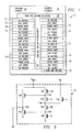
- FIGURE 8 is a flow chart of a programming algorithm common in the industry.
- the algorithm starts at 250.
- V cc the read voltage
- Vpp the programming voltage
- An address pointer is initially set to a first memory location at step 254.
- a counter X is set at zero at step 256.
- the contents of one word are verified. If however the cells in the word which are to be programmed to a "0" fail to correctly register a zero, the word fails and the algorithm passes to step 264. X is incremented at this step.
- the counter X is compared to a predetermined number, such as 10, to determine if this number of programming attempts have been made.
- step 268 determines whether the device has failed. If X is now equal to 10, a determination is made that the device has failed at step 268. If X is not yet equal to 10 or some other predetermined number, the program proceeds to step 269, which programs the selected cells in the word with a one millisecond pulse. This loop continues until the word passes or until 10 has been reached by the counter X.
- the algorithm asks whether the current address is equal to the last address. If not, the address is incremented at step 272 and the program loops back to step 256, where the counter X is again set to "0" for a next programming cycle. If the last address has been reached, then V pp is set back to five volts plus or minus ten percent at step 274. At step 276, all bytes are compared to the original data to be programmed. It is at this point that pattern sensitivity has been detected in some instances, wherein some cells have been thought to pass a "0" but later have been determined to fail. This will be explained in more detail below. Finally, if all of the bytes of the original data have passed, the device passes at step 278.
- Transistor 214 will be considered nonconductive where it cannot pass enough current to pull BL1 down.
- the voltage at node BL1 is replenished by i220 from the source V bias and i216 (running in a direction opposite from that shown) from the array source AS2.
- the leakage current through transistor 214 may be higher in the presence of a large i216, and the sense amplifier will still "see” a high level at BL1. Therefore, the amount of charge on the floating gate 238 of transistor 214, in order for the sense amplifier to sense a "0" on BL1, need not be as great as if there were no contribution from i216.
- the conventional programming algorithm as shown in FIGURE 8 steps from one cell to the next cell in the same row.
- transistors 214 and 216 require to be programmed with "zeros". If transistor 216 is programmed with a zero, the current i216 will decrease. Therefore, in reading cell 214, the voltage on BL1 will not be replenished sufficiently by i216, and i220 will not be able to keep up with the leakage current through the current path of transistor 214. The voltage on BL1 will be drained off to a low state. The sense amplifier, when reading BL1, will sense a "1", which is error.
- One solution to this pattern sensitivity problem is to program each cell that is to receive a "0" state with one pulse. This significantly increases the resistance of the current path of the cells so programmed, such that there will not be as significant a current contribution from a neighboring, zero-programmed cell as there was in the conventional algorithm. After all zero-programmed cells have received one pulse, the program loops back and programs each "zero" cell with a remaining number of pulses to bring the charge up on that cell's floating gate until a "0" is read.
- the conventional algorithm as shown in FIGURE 8 has been accepted as an industry standard, and this alternative programming method is therefore not always available as a choice for solving the pattern sensitivity problem.
- a solution to this pattern sensitivity problem is to turn off all inverse virtual ground signals for the array as described in FIGURE 7.
- VG1 and VG2 are turned off only in the program verify mode, or step 262 in FIGURE 8. This isolates AS1, AS2... from the voltage bias source.
- VG1 is turned on, rendering the current path of transistor 230 conductive and connecting AS1 to a ground path.
- the state of BL1 is then sensed. Because VG2 has been turned off, AS2 will no longer be high. The current i216 will therefore be negligible and a correct reading at node BL1 will be had.
- the true virtual ground signals, VG1, VG2... are still independently selectable, such that a selected one of the virtual ground signals is turned on while the rest are turned off.
- Signal Z a decoded signal, is on in both read and verify states.
- the inverse program enable signal PE is also high in both read and verify states, while signal Z is low in both of these states.
- the signal SAT is at VCCRB in a read state, while the signal SAT is in a nonzero, impedance-reducing state in the verify mode.
- node 140 Since, in the verify mode, transistor 135 is off and the impedance of transistor 133 has been reduced, the voltage level at node 134 causes p-channel transistor 138 to be rendered nonconductive. Node 140 therefore is not a source of current for the array source node or the current path of the nonselected cell associated with it.
- FIGURES 4-6 are signal generating circuits which together partially comprise a circuit for sensing the presence of a read or a verify state, among other states.
- the program enable signal PE is low while its inverse is high.
- the D signal is set at RB, a nonzero voltage bias source, while in the verify state, the signal is low.
- RB is in both read and verify states equivalent to V bias V t .
- the signal WE is low, while in the verify state, WE is high, and the reverse states are true for its inverse, WE .
- the receipt of the DATA and WE signals by the circuitry shown in FIGURES 4 and 6 allow the differentiation of read and program verify states.
Landscapes
- Read Only Memory (AREA)
- For Increasing The Reliability Of Semiconductor Memories (AREA)
Applications Claiming Priority (2)
| Application Number | Priority Date | Filing Date | Title |
|---|---|---|---|
| US45071389A | 1989-12-14 | 1989-12-14 | |
| US450713 | 1989-12-14 |
Publications (2)
| Publication Number | Publication Date |
|---|---|
| EP0432481A2 true EP0432481A2 (fr) | 1991-06-19 |
| EP0432481A3 EP0432481A3 (en) | 1992-04-29 |
Family
ID=23789204
Family Applications (1)
| Application Number | Title | Priority Date | Filing Date |
|---|---|---|---|
| EP19900121675 Withdrawn EP0432481A3 (en) | 1989-12-14 | 1990-11-13 | Methods and apparatus for verifying the state of a plurality of electrically programmable memory cells |
Country Status (3)
| Country | Link |
|---|---|
| US (1) | US5124945A (fr) |
| EP (1) | EP0432481A3 (fr) |
| JP (1) | JPH03230400A (fr) |
Cited By (3)
| Publication number | Priority date | Publication date | Assignee | Title |
|---|---|---|---|---|
| US5270131A (en) * | 1990-12-11 | 1993-12-14 | Sulzer Brothers Limited | Module for a fuel cell battery |
| GB2296589A (en) * | 1994-12-29 | 1996-07-03 | Hyundai Electronics Ind | Sensing circuit for a memory cell |
| EP0782148A3 (fr) * | 1995-12-29 | 1999-04-14 | STMicroelectronics S.r.l. | Méthode pour prévenir des perturbations pendant la programmation et l'effacementd'une mémoire non-volatile |
Families Citing this family (21)
| Publication number | Priority date | Publication date | Assignee | Title |
|---|---|---|---|---|
| JPH04188498A (ja) * | 1990-11-22 | 1992-07-07 | Fujitsu Ltd | 書き換え可能な不揮発性半導体記憶装置 |
| DE4205061C2 (de) * | 1991-02-19 | 2000-04-06 | Toshiba Kawasaki Kk | Nichtflüchtige Halbleiter-Speicheranordnung |
| US5457696A (en) * | 1991-08-08 | 1995-10-10 | Matsushita Electric Industrial Co., Ltd. | Semiconductor memory having internal test circuit |
| US5224070A (en) * | 1991-12-11 | 1993-06-29 | Intel Corporation | Apparatus for determining the conditions of programming circuitry used with flash EEPROM memory |
| US5361227A (en) | 1991-12-19 | 1994-11-01 | Kabushiki Kaisha Toshiba | Non-volatile semiconductor memory device and memory system using the same |
| US6781895B1 (en) * | 1991-12-19 | 2004-08-24 | Kabushiki Kaisha Toshiba | Non-volatile semiconductor memory device and memory system using the same |
| JP2812039B2 (ja) * | 1992-02-28 | 1998-10-15 | 日本電気株式会社 | 電気的に書込み・消去可能な不揮発性半導体記憶装置 |
| US5347489A (en) * | 1992-04-21 | 1994-09-13 | Intel Corporation | Method and circuitry for preconditioning shorted rows in a nonvolatile semiconductor memory incorporating row redundancy |
| JPH06139786A (ja) * | 1992-10-27 | 1994-05-20 | Fujitsu Ltd | 電気的消去及び書込み可能rom |
| JP3737525B2 (ja) * | 1994-03-11 | 2006-01-18 | 株式会社東芝 | 半導体記憶装置 |
| KR0142364B1 (ko) * | 1995-01-07 | 1998-07-15 | 김광호 | 소거된 메모리 쎌의 임계전압 마아진 확보를 위한 공통 소오스라인 구동회로 |
| JP3200012B2 (ja) * | 1996-04-19 | 2001-08-20 | 株式会社東芝 | 記憶システム |
| FR2756658B1 (fr) * | 1996-11-29 | 1999-01-22 | Sgs Thomson Microelectronics | Memoire electronique non volatile et son procede de gestion |
| US6999345B1 (en) | 2002-11-06 | 2006-02-14 | Halo Lsi, Inc. | Method of sense and program verify without a reference cell for non-volatile semiconductor memory |
| WO2007069322A1 (fr) * | 2005-12-15 | 2007-06-21 | Spansion Llc | Dispositif a semi-conducteurs et procede associe pour le commander |
| US7440331B2 (en) * | 2006-06-01 | 2008-10-21 | Sandisk Corporation | Verify operation for non-volatile storage using different voltages |
| US7457163B2 (en) * | 2006-06-01 | 2008-11-25 | Sandisk Corporation | System for verifying non-volatile storage using different voltages |
| US7450421B2 (en) * | 2006-06-02 | 2008-11-11 | Sandisk Corporation | Data pattern sensitivity compensation using different voltage |
| US7310272B1 (en) * | 2006-06-02 | 2007-12-18 | Sandisk Corporation | System for performing data pattern sensitivity compensation using different voltage |
| KR102124209B1 (ko) * | 2014-04-14 | 2020-06-18 | 삼성전자주식회사 | 반도체 메모리 장치 |
| CN116959544B (zh) * | 2023-09-20 | 2023-12-15 | 上海芯存天下电子科技有限公司 | 校验电流的设置方法、操作校验方法及相关设备 |
Family Cites Families (13)
| Publication number | Priority date | Publication date | Assignee | Title |
|---|---|---|---|---|
| US4021781A (en) * | 1974-11-19 | 1977-05-03 | Texas Instruments Incorporated | Virtual ground read-only-memory for electronic calculator or digital processor |
| US4301535A (en) * | 1979-07-02 | 1981-11-17 | Mostek Corporation | Programmable read only memory integrated circuit with bit-check and deprogramming modes and methods for programming and testing said circuit |
| IT1224062B (it) * | 1979-09-28 | 1990-09-26 | Ates Componenti Elettron | Metodo di programmazione per una memoria a semiconduttore non volatile elettricamente alterabile |
| US4281397A (en) * | 1979-10-29 | 1981-07-28 | Texas Instruments Incorporated | Virtual ground MOS EPROM or ROM matrix |
| US4301518A (en) * | 1979-11-01 | 1981-11-17 | Texas Instruments Incorporated | Differential sensing of single ended memory array |
| US4460981A (en) * | 1981-12-24 | 1984-07-17 | Intel Corporation | Virtual ground memory |
| US4460982A (en) * | 1982-05-20 | 1984-07-17 | Intel Corporation | Intelligent electrically programmable and electrically erasable ROM |
| JPH051040Y2 (fr) * | 1985-04-09 | 1993-01-12 | ||
| US4722075A (en) * | 1985-10-15 | 1988-01-26 | Texas Instruments Incorporated | Equalized biased array for PROMS and EPROMS |
| US4723225A (en) * | 1985-10-15 | 1988-02-02 | Texas Instruments Incorporated | Programming current controller |
| JPS62229600A (ja) * | 1986-03-31 | 1987-10-08 | Toshiba Corp | 不揮発性半導体記憶装置 |
| JPH0715799B2 (ja) * | 1987-06-30 | 1995-02-22 | 日本電気株式会社 | 半導体記憶装置 |
| US4868790A (en) * | 1988-04-28 | 1989-09-19 | Texas Instruments Incorporated | Reference circuit for integrated memory arrays having virtual ground connections |
-
1990
- 1990-11-13 EP EP19900121675 patent/EP0432481A3/en not_active Withdrawn
- 1990-11-30 JP JP2337032A patent/JPH03230400A/ja active Pending
-
1991
- 1991-07-29 US US07/737,830 patent/US5124945A/en not_active Expired - Lifetime
Cited By (5)
| Publication number | Priority date | Publication date | Assignee | Title |
|---|---|---|---|---|
| US5270131A (en) * | 1990-12-11 | 1993-12-14 | Sulzer Brothers Limited | Module for a fuel cell battery |
| GB2296589A (en) * | 1994-12-29 | 1996-07-03 | Hyundai Electronics Ind | Sensing circuit for a memory cell |
| GB2296589B (en) * | 1994-12-29 | 1999-06-23 | Hyundai Electronics Ind | Sensing circuit to enhance sensing margin |
| EP0782148A3 (fr) * | 1995-12-29 | 1999-04-14 | STMicroelectronics S.r.l. | Méthode pour prévenir des perturbations pendant la programmation et l'effacementd'une mémoire non-volatile |
| US6195290B1 (en) | 1995-12-29 | 2001-02-27 | Stmicroelectronics S.R.L. | Method of avoiding disturbance during the step of programming and erasing an electrically programmable, semiconductor non-volatile storage device |
Also Published As
| Publication number | Publication date |
|---|---|
| US5124945A (en) | 1992-06-23 |
| JPH03230400A (ja) | 1991-10-14 |
| EP0432481A3 (en) | 1992-04-29 |
Similar Documents
| Publication | Publication Date | Title |
|---|---|---|
| US5124945A (en) | Method and apparatus for verifying the state of a plurality of electrically programmable memory cells | |
| US4779272A (en) | Testable variable-threshold non-volatile semiconductor memory | |
| KR0172408B1 (ko) | 다수상태 불휘발성 반도체 메모리 및 그의 구동방법 | |
| KR100284916B1 (ko) | 반도체 기억 장치 및 그 기입 제어 방법 | |
| US5790459A (en) | Memory circuit for performing threshold voltage tests on cells of a memory array | |
| EP0480752B1 (fr) | Dispositif de mémoire à semiconducteur comprenant des moyens d'identification de court circuits | |
| US5748545A (en) | Memory device with on-chip manufacturing and memory cell defect detection capability | |
| US5742615A (en) | Non-volatile semiconductor memory | |
| US6859401B2 (en) | Fail number detecting circuit of flash memory | |
| US6525960B2 (en) | Nonvolatile semiconductor memory device including correction of erratic memory cell data | |
| US5954828A (en) | Non-volatile memory device for fault tolerant data | |
| USRE44350E1 (en) | Nonvolatile semiconductor memory including multi-threshold voltage memory cells including voltage ranges indicating either an erase state or a two or more program state | |
| EP0662692B1 (fr) | Dispositif de mémoire à semi-conducteurs non volatile | |
| EP0239968A2 (fr) | Dispositif de mémoire semi-conductrice non volatile | |
| US5684741A (en) | Auto-verification of programming flash memory cells | |
| US5959890A (en) | Non-volatile semiconductor memory device | |
| EP0436814A2 (fr) | Méthode et appareil pour lire et programmer des cellules de mémoire électriquement programmables | |
| US5491662A (en) | Microcontroller memory cell current reading method | |
| US7564724B2 (en) | Flash memory device | |
| KR19980071781A (ko) | 모든 메모리셀에 대해 소거 베리파이 동작이 일괄적으로 정확히 행해질 수 있는 반도체기억장치 | |
| KR20000005054A (ko) | 테스트 회로를 갖춘 회로장치 | |
| US20030095438A1 (en) | Nonvolatile semiconductor memory device having function of determining good sector | |
| US5812460A (en) | Nonvolatile semiconductor memory device having test circuit for testing erasing function thereof | |
| JP3346850B2 (ja) | 不揮発性半導体メモリ | |
| KR0172440B1 (ko) | 테스트 시간을 감소시킨 불휘발성 반도체 메모리 장치 |
Legal Events
| Date | Code | Title | Description |
|---|---|---|---|
| PUAI | Public reference made under article 153(3) epc to a published international application that has entered the european phase |
Free format text: ORIGINAL CODE: 0009012 |
|
| AK | Designated contracting states |
Kind code of ref document: A2 Designated state(s): DE FR GB IT NL |
|
| PUAL | Search report despatched |
Free format text: ORIGINAL CODE: 0009013 |
|
| AK | Designated contracting states |
Kind code of ref document: A3 Designated state(s): DE FR GB IT NL |
|
| 17P | Request for examination filed |
Effective date: 19930108 |
|
| 17Q | First examination report despatched |
Effective date: 19940801 |
|
| STAA | Information on the status of an ep patent application or granted ep patent |
Free format text: STATUS: THE APPLICATION IS DEEMED TO BE WITHDRAWN |
|
| 18D | Application deemed to be withdrawn |
Effective date: 19950214 |