EP0432963A2 - Méthode et appareil pour l'évaluation de niveaux de dopage par implantation d'ions dans des semi-conducteurs - Google Patents
Méthode et appareil pour l'évaluation de niveaux de dopage par implantation d'ions dans des semi-conducteurs Download PDFInfo
- Publication number
- EP0432963A2 EP0432963A2 EP90313222A EP90313222A EP0432963A2 EP 0432963 A2 EP0432963 A2 EP 0432963A2 EP 90313222 A EP90313222 A EP 90313222A EP 90313222 A EP90313222 A EP 90313222A EP 0432963 A2 EP0432963 A2 EP 0432963A2
- Authority
- EP
- European Patent Office
- Prior art keywords
- material layer
- dosage level
- thickness
- probe
- radiation
- Prior art date
- Legal status (The legal status is an assumption and is not a legal conclusion. Google has not performed a legal analysis and makes no representation as to the accuracy of the status listed.)
- Granted
Links
- 239000004065 semiconductor Substances 0.000 title claims description 32
- 238000000034 method Methods 0.000 title claims description 19
- 239000007943 implant Substances 0.000 title claims description 14
- 239000011248 coating agent Substances 0.000 claims abstract 6
- 238000000576 coating method Methods 0.000 claims abstract 6
- 239000000523 sample Substances 0.000 claims description 100
- 238000005259 measurement Methods 0.000 claims description 33
- 229910021417 amorphous silicon Inorganic materials 0.000 claims description 31
- 239000000463 material Substances 0.000 claims description 19
- 230000005855 radiation Effects 0.000 claims description 19
- 238000002513 implantation Methods 0.000 claims description 7
- 229910021419 crystalline silicon Inorganic materials 0.000 claims description 5
- 230000002596 correlated effect Effects 0.000 claims description 4
- IJGRMHOSHXDMSA-UHFFFAOYSA-N Atomic nitrogen Chemical compound N#N IJGRMHOSHXDMSA-UHFFFAOYSA-N 0.000 abstract 12
- 239000002904 solvent Substances 0.000 abstract 7
- 229910052757 nitrogen Inorganic materials 0.000 abstract 6
- 239000007788 liquid Substances 0.000 abstract 3
- 238000011084 recovery Methods 0.000 abstract 3
- 239000012530 fluid Substances 0.000 abstract 2
- 239000006200 vaporizer Substances 0.000 abstract 2
- 238000007599 discharging Methods 0.000 abstract 1
- 238000001704 evaporation Methods 0.000 abstract 1
- 239000002808 molecular sieve Substances 0.000 abstract 1
- URGAHOPLAPQHLN-UHFFFAOYSA-N sodium aluminosilicate Chemical compound [Na+].[Al+3].[O-][Si]([O-])=O.[O-][Si]([O-])=O URGAHOPLAPQHLN-UHFFFAOYSA-N 0.000 abstract 1
- 239000012808 vapor phase Substances 0.000 abstract 1
- 150000002500 ions Chemical class 0.000 description 13
- 238000002310 reflectometry Methods 0.000 description 13
- 230000003287 optical effect Effects 0.000 description 11
- 238000013459 approach Methods 0.000 description 10
- 230000000694 effects Effects 0.000 description 10
- 238000005468 ion implantation Methods 0.000 description 9
- XKRFYHLGVUSROY-UHFFFAOYSA-N Argon Chemical compound [Ar] XKRFYHLGVUSROY-UHFFFAOYSA-N 0.000 description 8
- 238000013178 mathematical model Methods 0.000 description 5
- XUIMIQQOPSSXEZ-UHFFFAOYSA-N Silicon Chemical compound [Si] XUIMIQQOPSSXEZ-UHFFFAOYSA-N 0.000 description 4
- 229910052786 argon Inorganic materials 0.000 description 4
- 229910052710 silicon Inorganic materials 0.000 description 4
- 239000010703 silicon Substances 0.000 description 4
- 238000012360 testing method Methods 0.000 description 4
- 235000012431 wafers Nutrition 0.000 description 4
- 238000004364 calculation method Methods 0.000 description 3
- 229910052785 arsenic Inorganic materials 0.000 description 2
- 229910052796 boron Inorganic materials 0.000 description 2
- -1 boron ions Chemical class 0.000 description 2
- 230000007547 defect Effects 0.000 description 2
- 238000001514 detection method Methods 0.000 description 2
- CPBQJMYROZQQJC-UHFFFAOYSA-N helium neon Chemical compound [He].[Ne] CPBQJMYROZQQJC-UHFFFAOYSA-N 0.000 description 2
- 238000002955 isolation Methods 0.000 description 2
- 230000007246 mechanism Effects 0.000 description 2
- 238000012544 monitoring process Methods 0.000 description 2
- 230000010287 polarization Effects 0.000 description 2
- 230000008569 process Effects 0.000 description 2
- 230000004044 response Effects 0.000 description 2
- JBRZTFJDHDCESZ-UHFFFAOYSA-N AsGa Chemical compound [As]#[Ga] JBRZTFJDHDCESZ-UHFFFAOYSA-N 0.000 description 1
- ZOXJGFHDIHLPTG-UHFFFAOYSA-N Boron Chemical compound [B] ZOXJGFHDIHLPTG-UHFFFAOYSA-N 0.000 description 1
- 238000002441 X-ray diffraction Methods 0.000 description 1
- 238000010521 absorption reaction Methods 0.000 description 1
- 238000005280 amorphization Methods 0.000 description 1
- 238000000137 annealing Methods 0.000 description 1
- RQNWIZPPADIBDY-UHFFFAOYSA-N arsenic atom Chemical compound [As] RQNWIZPPADIBDY-UHFFFAOYSA-N 0.000 description 1
- HAYXDMNJJFVXCI-UHFFFAOYSA-N arsenic(5+) Chemical compound [As+5] HAYXDMNJJFVXCI-UHFFFAOYSA-N 0.000 description 1
- 230000008859 change Effects 0.000 description 1
- 239000002178 crystalline material Substances 0.000 description 1
- 230000001419 dependent effect Effects 0.000 description 1
- 238000010586 diagram Methods 0.000 description 1
- 239000012776 electronic material Substances 0.000 description 1
- 238000011156 evaluation Methods 0.000 description 1
- BHEPBYXIRTUNPN-UHFFFAOYSA-N hydridophosphorus(.) (triplet) Chemical compound [PH] BHEPBYXIRTUNPN-UHFFFAOYSA-N 0.000 description 1
- 238000003384 imaging method Methods 0.000 description 1
- 238000004519 manufacturing process Methods 0.000 description 1
- 238000012986 modification Methods 0.000 description 1
- 230000004048 modification Effects 0.000 description 1
- 230000003534 oscillatory effect Effects 0.000 description 1
- 238000012552 review Methods 0.000 description 1
- 230000035945 sensitivity Effects 0.000 description 1
- 239000000758 substrate Substances 0.000 description 1
- 230000001360 synchronised effect Effects 0.000 description 1
Images

Classifications
-
- G—PHYSICS
- G01—MEASURING; TESTING
- G01N—INVESTIGATING OR ANALYSING MATERIALS BY DETERMINING THEIR CHEMICAL OR PHYSICAL PROPERTIES
- G01N21/00—Investigating or analysing materials by the use of optical means, i.e. using sub-millimetre waves, infrared, visible or ultraviolet light
- G01N21/17—Systems in which incident light is modified in accordance with the properties of the material investigated
- G01N21/1717—Systems in which incident light is modified in accordance with the properties of the material investigated with a modulation of one or more physical properties of the sample during the optical investigation, e.g. electro-reflectance
-
- G—PHYSICS
- G01—MEASURING; TESTING
- G01N—INVESTIGATING OR ANALYSING MATERIALS BY DETERMINING THEIR CHEMICAL OR PHYSICAL PROPERTIES
- G01N21/00—Investigating or analysing materials by the use of optical means, i.e. using sub-millimetre waves, infrared, visible or ultraviolet light
- G01N21/17—Systems in which incident light is modified in accordance with the properties of the material investigated
- G01N21/1702—Systems in which incident light is modified in accordance with the properties of the material investigated with opto-acoustic detection, e.g. for gases or analysing solids
-
- G—PHYSICS
- G01—MEASURING; TESTING
- G01N—INVESTIGATING OR ANALYSING MATERIALS BY DETERMINING THEIR CHEMICAL OR PHYSICAL PROPERTIES
- G01N21/00—Investigating or analysing materials by the use of optical means, i.e. using sub-millimetre waves, infrared, visible or ultraviolet light
- G01N21/84—Systems specially adapted for particular applications
- G01N21/88—Investigating the presence of flaws or contamination
- G01N21/95—Investigating the presence of flaws or contamination characterised by the material or shape of the object to be examined
- G01N21/9501—Semiconductor wafers
- G01N21/9505—Wafer internal defects, e.g. microcracks
-
- G—PHYSICS
- G01—MEASURING; TESTING
- G01R—MEASURING ELECTRIC VARIABLES; MEASURING MAGNETIC VARIABLES
- G01R31/00—Arrangements for testing electric properties; Arrangements for locating electric faults; Arrangements for electrical testing characterised by what is being tested not provided for elsewhere
- G01R31/28—Testing of electronic circuits, e.g. by signal tracer
- G01R31/302—Contactless testing
- G01R31/308—Contactless testing using non-ionising electromagnetic radiation, e.g. optical radiation
Definitions
- the subject apparatus is for evaluating the ion implant dosage level in semiconductor samples.
- the apparatus is particularly suited for evaluating samples having high dosage levels.
- Most semiconductor fabrication techniques include one or more ion implantation process steps. In order to maintain high yields, the ion implantation must be accurately controlled.
- a number of different approaches have been developed for measuring the dosage level in a semiconductor sample. One particularly advantageous approach is based upon the measurement of a modulated reflectance signal which can be related to the dosage level.
- a modulated reflectance signal is obtained by periodically exciting the semiconductor sample with a focused, intensity modulated, pump laser beam. A probe beam is then reflected off the surface of the sample within the periodically excited area. The reflected power of the probe beam is measured to yield the modulated reflectance signal. This measurement is then correlated with the dosage level.
- Therma-Probe device is being widely used by the semiconductor industry to monitor all types of ion implant processes. Up until now, this device has been limited to monitoring dosage levels up to 1014 to 1015 ions/cm2. Some semiconductor manufacturers are now using higher doses, up to 1016 ions/cm2.
- the difficulty in extending the sensitivity of the device to the highest dosage levels is due principally to the fact that the rise in the measured modulated reflectance signal, which is monotonic below 1014 ions/cm2 and can therefore be directly correlated with dosage level, becomes oscillatory at higher dosage levels.
- the reason for this change in behavior in the modulated reflected signal has been attributed to the fact that the high level of ion implantation transforms the crystalline material into amorphous silicon.
- Amorphous silicon is created when more than ten percent of the atoms in the lattice structure are displaced.
- Amorphous silicon is characterized by the fact that no x-ray diffraction patterns can be generated since the lattice has been so severely disturbed.
- a layer of amorphous silicon is created which lies just below an upper layer of less damaged silicon.
- the reason there is a layer of damaged (but still crystalline) silicon above the amorphous silicon layer depends upon the type of ions which are being implanted. For example, implantation using the arsenic ion requires relatively high energies. Some of this implantation energy is transferred to the material near the upper surface of the sample creating a dynamic annealing effect which recreates the crystalline structure.
- a different scenario occurs in boron implantation. More specifically, the boron ions are implanted with very high speed and literally pass through the upper layer before they have slowed down enough to interact with the lattice in an amount sufficient to create amorphous silicon. In either case, the result of high dosage implantation is to create an upper layer of damaged, crystalline silicon and an intermediate layer of amorphous silicon below.
- the latter article also describes how the thickness of the amorphous silicon layer can be related to the level of ion implantation. More specifically, as the level of ion implantation increases to high dosages, the thickness of the amorphous silicon layer will increase.
- the latter article also includes calculations indicating how both the modulated and non-modulated reflectance signals of a probe beam will behave as the thickness of the amorphous silicon layer increases. [See also “Modulated Optical Reflectance Measurements on Amorphous Silicon Layers and Detection of Residual Defects", S. Wurm, P. Alpern, D. Savignac, and R. Kakoschke, Appl. Phys. A 47 , 147-155 (1988).]
- a typical implanted semiconductor sample consists of a number of layers each having an unknown thickness.
- a typical sample includes an upper damaged crystalline layer and a lower layer of amorphous silicon.
- the subject apparatus and method provides for the measurement of three independent reflectivities.
- the first measurement is defined by the above described modulated reflectance signal of a probe beam.
- the second measurement is of the non-modulated reflectance signal of the probe beam.
- the third measurement is defined by the non-modulated reflectance of a separate beam, having a wavelength different than the probe beam.
- the principal components of the subject apparatus are similar to those found in the above mentioned Therma-Probe device and described in the above cited patents which discuss the measurement of thermal and plasma waves in semiconductors. The principal difference is that the measurements which can be obtained are now utilized in a novel manner to produce a new result not heretofore disclosed or contemplated.
- the subject apparatus includes an intensity modulated pump laser for exciting the semiconductor sample.
- a probe beam having a different wavelength than the pump beam is focussed with the pump beam to a substantially coincident spot on the surface of the sample.
- a first photodetector is providing for measuring the modulated reflected power of the probe beam.
- the modulated reflected power is based on the signal which is in phase with the intensity modulated pump beam.
- the second independent measurement taken is the non-modulated reflected power of the probe beam.
- this second measurement can be made using the same photodetector element which measured the modulated reflected power of the probe beam.
- a third independent reflectivity measurement is also made.
- This third reflectance signal consists of the non-modulated power of the pump beam.
- a separate photodetector is used for this purpose. As noted above, these three independent measurements can be used to evaluate the dosage level in the semiconductor sample.
- the non-modulated reflected power of both the pump and probe beams have been measured. These measurements were taken in order to normalize the modulated reflectance signal. More specifically, the non-modulated pump and probe beam reflected powers must be measured to normalize the modulated probe beam reflectance signal so that any effects of absorption of the pump and probe beam wavelengths in the sample can be cancelled. In certain models of the prior art Therma-Probe device, the non-modulated reflected power of the pump beam is also used to help locate areas of interest on the semiconductor sample. This approach is described in U.S. Patent No. 4,795,260 issued January 3, 1989 and also assigned to the assignee of the subject invention. While the non-modulated reflective pump and probe beam powers have been measured and utilized in the prior art, there has never been any effort to utilize those measurements in combination to derive information about ion implantation levels as described in greater detail below.
- Figure 1 is a block diagram of the subject invention.
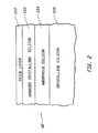
- Figure 2 is a cross-sectional, schematic view of a sample semiconductor.
- the device 10 includes a pump laser 20 which may be an argon laser with a 488 nm, 35 Mw output beam 22.
- An acousto-optic modulator 24 is provided for intensity modulating the output beam 22 of pump laser 20.
- the modulation frequency is on the order of 1-10 MHz.
- the intensity modulated beam 22 is then passed through a beam expander 26 and an isolator 28 for preventing feedback into the pump laser cavity.
- the beam then passes through splitter 32 discussed below.
- a turning mirror 33 is illustrated for convenience.
- the beam 22 is then passed through a quarter waveplate optical rotator 30.
- a dichroic mirror 34 which reflects the argon radiation is then used to redirect the beam downwardly through a second dichroic mirror 36 which is transparent to the argon radiation.
- the beam is then focussed by a microscope objective 40 onto the surface of a semiconductor sample 42 with an incident power of about 10 mW.
- An autofocus mechanism 44 is provided to maintain a spot size resolution of about 1 micron in diameter.
- the intensity modulated pump laser beam functions to periodically excite the sample creating plasma and thermal waves.
- the sample rests on a movable stage.
- the upper stage level 50 provides rotation about an angle ⁇ and the lower two stages 52 and 54 provide x and y motion respectively.
- the subject apparatus 10 further includes a probe laser 60 for emitting a beam 62.
- Probe laser 60 is preferably a linearly polarized helium neon laser generating a 633 nm beam 62 having a 5 mW power output.
- Beam 62 is passed through a beam expander 64 and a splitter element 66.
- the beam is then passed through a quarter waveplate 68 and is reflected downwardly to the sample surface by dichroic mirror 36 with an incident power of about 3 mW.
- the pump and probe beams are focussed in a substantially coincident manner on the surface of the sample to maximize the reflectivity signal.
- a vision system is provided to help view the sample.
- the vision system includes a white light source 70 which is directed to the sample by turning mirror 72 through a splitter 74 and through the dichroic mirrors 34 and 36. The returning light is redirected by the splitter 74 to a camera 76.
- three independent reflectivity measurements are made in order to derive information about the ion implantation dosage level of the sample 42. These measurements include the modulated and non-modulated reflected power of the probe beam 62 as well as the non-modulated reflected power of the pump beam 22. The elements utilized to obtain these measurements are disclosed below.
- the reflected probe beam is redirected by mirror 36 through quarter waveplate 68.
- the second pass through the quarter waveplate 68 functions to rotate the polarization of the beam a full 90° so that when the beam reaches splitter 66 it is redirected upwardly towards photodetector 80.
- the reflected probe beam 62 Prior to reaching photodetector 80, the reflected probe beam 62 will pass through a splitter 82 and an isolation filter 84.
- Isolation filter 84 is designed to shield photodetector 80 from any stray argon pump radiation.
- Splitter 82 functions to pick off a small portion of the beam and redirect it to an autofocus mechanism 86.
- Photodetector 80 is designed to measure the reflected power of the probe beam. This result is achieved by making sure that the probe beam underfills the surface of the photodetector. In this manner, photodetector 80 measures only the modulations in the reflected power and is insensitive to any small variations in probe beam diameter or position that are induced by thermal lens effects or thermo-elastic deformations at the sample surface. The photodetector functions to generate a voltage proportional to the power of the beam falling on its surface. This signal is then supplied to a processor 90. The DC component of the voltage signal supplied to the processor defines the non-modulated probe beam reflectance.
- Processor 90 is connected to modulator 24 so that a phase-sensitive synchronous detection system can be used to measure modulated reflectance changes at 1-10 Mhz frequencies as small as 10 ⁇ 7/ ⁇ Hz.
- the output from photodetector 80 is used by the processor to derive both the modulated and non-modulated reflected powers of the probe beam.
- the third remaining independent reflectivity measurement is of the non-modulated pump beam power.
- the reflected pump beam 22 is redirected back through quarterwaveplate 30 by dichroic mirror 34.
- the second pass through the quarter waveplate 30 functions to rotate the polarization of the beam a full 90° so that the bulk of the reflected pump power can be reflected out of the system by isolator 28.
- Splitter 32 is provided to pick-off a small portion (approximately 4%) of the reflected pump beam radiation.
- This pump beam radiation is passed through a filter 94 for isolating the helium neon probe radiation prior to reaching detector 96.
- the pump beam is arranged to underfill the surface of photodetector 96 for the reasons discussed above.
- the output voltage from detector 96 is supplied to processor 90 and the DC component of that voltage is used to derive the non-modulated power of the reflected pump beam.
- two additional photodetectors and optical pick-offs are provided for measuring the incident powers of the pump and probe beams.
- the incident beam power is measured to correct for variations in the power of the lasers.
- the processor can then determine the thickness of the amorphous silicon layer which, in turn, can be related to the dosage level in the sample.
- the mathematical approach can best be understood by referring to Figure 2 which shows a cross-section of the upper surface of a semiconductor sample 42. As shown in Figure 2, the upper surface of the sample includes a thin oxide layer 110. Just below the oxide layer is a layer 112 of damaged crystalline silicon. Below that crystalline layer is a layer of amorphous silicon 114. The remainder of the sample is shown as 116.
- each of the layers 110, 112, and 114 is unknown.
- a mathematical model can be developed which relates the reflectivity of the sample to the thickness of these layers using well-known Fresnel equations. The equations which are utilized for this specific approach are set forth below.
- r n is a characteristic reflection coefficient defined by where k n is the optical wave vector ⁇ is the probe beam wavelength and d n is the thickness of the n th layer and where N n and K n are, respectively, the real and imaginary parts of the complex refractive index.
- the reflectance R is simply the square of the magnitude of ⁇ o .
- the first term in Eq. (2) describes the modulation in the optical contrast at the layer boundaries.
- the second term is essentially the thermal lens effect known to occur anywhere in which there is a gradient in the optical properties of the material.
- the last term describes the effect of modulating the layer thickness either through thermal or plasma wave-induced expansion.
- the modulation of the reflectance ⁇ R is obtained by taking twice the real part of ⁇ o .
- the optimum solution for the thickness of the three unknown layers can be derived with a straight-forward least squares fitting technique. As noted above, if the thickness of the amorphous silicon layer is calculated, the dosage level can be derived.
- the actual dosage level of the sample is derived through calibration techniques.
- a plurality of test wafers are manufactured having various known dosage levels such as 1015, 2 x 10¹⁵, 5 x 10¹⁵ and 1016 ions/cm2.
- the measurements described above are taken on the test wafers. These measurements are used to calculate the thickness of the amorphous silicon layers formed in the test wafers. In practice, it has been found that the thickness of the amorphous silicon layer is roughly proportional to the ⁇ log Dose.
- the thickness of the ion-implantation-induced damaged layer is fixed in the model and the optical properties of the damaged layer are allowed to increase monotonically with dose over a range of values bounded by those of crystalline silicon and amorphous silicon.
- the subject approach can also be used to determine implant dosage levels of non-silicon based semiconductors such as the more recently developed gallium-arsenic semiconductors.
Landscapes
- Physics & Mathematics (AREA)
- General Physics & Mathematics (AREA)
- Health & Medical Sciences (AREA)
- Engineering & Computer Science (AREA)
- Immunology (AREA)
- Biochemistry (AREA)
- General Health & Medical Sciences (AREA)
- Analytical Chemistry (AREA)
- Chemical & Material Sciences (AREA)
- Pathology (AREA)
- Life Sciences & Earth Sciences (AREA)
- Computer Vision & Pattern Recognition (AREA)
- Electromagnetism (AREA)
- Toxicology (AREA)
- General Engineering & Computer Science (AREA)
- Testing Or Measuring Of Semiconductors Or The Like (AREA)
- Lasers (AREA)
Applications Claiming Priority (2)
| Application Number | Priority Date | Filing Date | Title |
|---|---|---|---|
| US07/448,882 US5074669A (en) | 1989-12-12 | 1989-12-12 | Method and apparatus for evaluating ion implant dosage levels in semiconductors |
| US448882 | 1989-12-12 |
Publications (3)
| Publication Number | Publication Date |
|---|---|
| EP0432963A2 true EP0432963A2 (fr) | 1991-06-19 |
| EP0432963A3 EP0432963A3 (en) | 1992-06-03 |
| EP0432963B1 EP0432963B1 (fr) | 1996-10-30 |
Family
ID=23782020
Family Applications (1)
| Application Number | Title | Priority Date | Filing Date |
|---|---|---|---|
| EP90313222A Expired - Lifetime EP0432963B1 (fr) | 1989-12-12 | 1990-12-05 | Méthode et appareil pour l'évaluation de niveaux de dopage par implantation d'ions dans des semi-conducteurs |
Country Status (4)
| Country | Link |
|---|---|
| US (1) | US5074669A (fr) |
| EP (1) | EP0432963B1 (fr) |
| JP (1) | JPH06101505B2 (fr) |
| DE (1) | DE69029027T2 (fr) |
Cited By (6)
| Publication number | Priority date | Publication date | Assignee | Title |
|---|---|---|---|---|
| WO1999001747A1 (fr) * | 1997-07-03 | 1999-01-14 | Therma-Wave, Inc. | Appareil d'analyse des couches metallisees de semiconducteurs |
| EP1007942A4 (fr) * | 1996-11-22 | 2000-06-14 | Perceptron Inc | Appareil de mesure d'un parametre physique et procede associe |
| US6128081A (en) * | 1996-11-22 | 2000-10-03 | Perceptron, Inc. | Method and system for measuring a physical parameter of at least one layer of a multilayer article without damaging the article and sensor head for use therein |
| EP1092123A4 (fr) * | 1998-06-30 | 2002-03-20 | Lockheed Corp | Technique et appareil permettant de detecter des deplacements supersoniques de surface par amplification optique post-detection |
| US6657733B1 (en) | 1998-06-30 | 2003-12-02 | Lockheed Martin Corporation | Method and apparatus for detecting ultrasonic surface displacements using post-collection optical amplification |
| WO2004048943A1 (fr) * | 2002-11-27 | 2004-06-10 | Optical Metrology Patents Limited | Spectrometre optique |
Families Citing this family (74)
| Publication number | Priority date | Publication date | Assignee | Title |
|---|---|---|---|---|
| US5172191A (en) * | 1991-08-06 | 1992-12-15 | The United States Of America As Represented By The Secretary Of The Army | Sweeping photoreflectance spectroscopy |
| US5185273A (en) * | 1991-09-30 | 1993-02-09 | Motorola, Inc. | Method for measuring ions implanted into a semiconductor substrate |
| JP3462272B2 (ja) * | 1994-09-07 | 2003-11-05 | 浜松ホトニクス株式会社 | アレイ電極基板の検査装置 |
| US5574562A (en) * | 1994-12-19 | 1996-11-12 | The Board Of Trustees Of The Leland Stanford Junior University | Method and apparatus for evaluation of high temperature superconductors |
| US5706094A (en) * | 1995-08-25 | 1998-01-06 | Brown University Research Foundation | Ultrafast optical technique for the characterization of altered materials |
| US6008906A (en) * | 1995-08-25 | 1999-12-28 | Brown University Research Foundation | Optical method for the characterization of the electrical properties of semiconductors and insulating films |
| US6321601B1 (en) | 1996-08-06 | 2001-11-27 | Brown University Research Foundation | Optical method for the characterization of laterally-patterned samples in integrated circuits |
| US5748318A (en) * | 1996-01-23 | 1998-05-05 | Brown University Research Foundation | Optical stress generator and detector |
| US6175416B1 (en) | 1996-08-06 | 2001-01-16 | Brown University Research Foundation | Optical stress generator and detector |
| US5844684A (en) * | 1997-02-28 | 1998-12-01 | Brown University Research Foundation | Optical method for determining the mechanical properties of a material |
| DE19781728B4 (de) * | 1996-04-26 | 2007-10-18 | Brown University Research Foundation | Optisches Verfahren und System zum Bestimmen mechanischer Eigenschaften eines Materials |
| US5748317A (en) * | 1997-01-21 | 1998-05-05 | Brown University Research Foundation | Apparatus and method for characterizing thin film and interfaces using an optical heat generator and detector |
| US5864393A (en) * | 1997-07-30 | 1999-01-26 | Brown University Research Foundation | Optical method for the determination of stress in thin films |
| WO1999013318A1 (fr) * | 1997-09-05 | 1999-03-18 | Brown University Research Foundation | Procede optique de caracterisation des proprietes electriques de semi-conducteurs et pellicules isolantes |
| US6049220A (en) | 1998-06-10 | 2000-04-11 | Boxer Cross Incorporated | Apparatus and method for evaluating a wafer of semiconductor material |
| US6054868A (en) * | 1998-06-10 | 2000-04-25 | Boxer Cross Incorporated | Apparatus and method for measuring a property of a layer in a multilayered structure |
| US6122060A (en) * | 1998-06-30 | 2000-09-19 | Lockheed Martin Corporation | Method and apparatus for detecting ultrasonic surface displacements using post-collection optical amplification |
| US6038026A (en) | 1998-07-07 | 2000-03-14 | Brown University Research Foundation | Apparatus and method for the determination of grain size in thin films |
| US6025918A (en) * | 1998-07-07 | 2000-02-15 | Brown University Research Foundation | Apparatus and method for measurement of the mechanical properties and electromigration of thin films |
| WO2000020841A1 (fr) | 1998-10-05 | 2000-04-13 | Kla-Tencor Corporation | Systeme interferometrique de mesure de perturbation d'un echantillon |
| US6595685B2 (en) * | 1998-10-13 | 2003-07-22 | National Research Laboratory Of Metrology | Method and apparatus for measuring thermophysical properties |
| US6323951B1 (en) | 1999-03-22 | 2001-11-27 | Boxer Cross Incorporated | Apparatus and method for determining the active dopant profile in a semiconductor wafer |
| US6268916B1 (en) | 1999-05-11 | 2001-07-31 | Kla-Tencor Corporation | System for non-destructive measurement of samples |
| US6317216B1 (en) | 1999-12-13 | 2001-11-13 | Brown University Research Foundation | Optical method for the determination of grain orientation in films |
| AU2884401A (en) * | 2000-01-28 | 2001-08-07 | Asahi Kasei Kabushiki Kaisha | Photothermic transducing spectroscopic analyzer |
| US6535285B1 (en) | 2000-02-08 | 2003-03-18 | Therma-Wave, Inc. | Combination thermal wave and optical spectroscopy measurement system |
| US6812047B1 (en) * | 2000-03-08 | 2004-11-02 | Boxer Cross, Inc. | Evaluating a geometric or material property of a multilayered structure |
| US6408048B2 (en) | 2000-03-14 | 2002-06-18 | Therma-Wave, Inc. | Apparatus for analyzing samples using combined thermal wave and X-ray reflectance measurements |
| US6462817B1 (en) | 2000-05-12 | 2002-10-08 | Carlos Strocchia-Rivera | Method of monitoring ion implants by examination of an overlying masking material |
| US6532070B1 (en) | 2000-07-17 | 2003-03-11 | Therma-Wave, Inc. | Method for determining ion concentration and energy of shallow junction implants |
| US6812045B1 (en) | 2000-09-20 | 2004-11-02 | Kla-Tencor, Inc. | Methods and systems for determining a characteristic of a specimen prior to, during, or subsequent to ion implantation |
| US6919957B2 (en) | 2000-09-20 | 2005-07-19 | Kla-Tencor Technologies Corp. | Methods and systems for determining a critical dimension, a presence of defects, and a thin film characteristic of a specimen |
| US6694284B1 (en) | 2000-09-20 | 2004-02-17 | Kla-Tencor Technologies Corp. | Methods and systems for determining at least four properties of a specimen |
| US6673637B2 (en) | 2000-09-20 | 2004-01-06 | Kla-Tencor Technologies | Methods and systems for determining a presence of macro defects and overlay of a specimen |
| US7106425B1 (en) | 2000-09-20 | 2006-09-12 | Kla-Tencor Technologies Corp. | Methods and systems for determining a presence of defects and a thin film characteristic of a specimen |
| US6633831B2 (en) | 2000-09-20 | 2003-10-14 | Kla Tencor Technologies | Methods and systems for determining a critical dimension and a thin film characteristic of a specimen |
| US7349090B2 (en) | 2000-09-20 | 2008-03-25 | Kla-Tencor Technologies Corp. | Methods and systems for determining a property of a specimen prior to, during, or subsequent to lithography |
| US6782337B2 (en) | 2000-09-20 | 2004-08-24 | Kla-Tencor Technologies Corp. | Methods and systems for determining a critical dimension an a presence of defects on a specimen |
| US6891627B1 (en) | 2000-09-20 | 2005-05-10 | Kla-Tencor Technologies Corp. | Methods and systems for determining a critical dimension and overlay of a specimen |
| US7130029B2 (en) | 2000-09-20 | 2006-10-31 | Kla-Tencor Technologies Corp. | Methods and systems for determining an adhesion characteristic and a thickness of a specimen |
| US6911349B2 (en) * | 2001-02-16 | 2005-06-28 | Boxer Cross Inc. | Evaluating sidewall coverage in a semiconductor wafer |
| US6812717B2 (en) * | 2001-03-05 | 2004-11-02 | Boxer Cross, Inc | Use of a coefficient of a power curve to evaluate a semiconductor wafer |
| US6940592B2 (en) * | 2001-10-09 | 2005-09-06 | Applied Materials, Inc. | Calibration as well as measurement on the same workpiece during fabrication |
| US6971791B2 (en) * | 2002-03-01 | 2005-12-06 | Boxer Cross, Inc | Identifying defects in a conductive structure of a wafer, based on heat transfer therethrough |
| US6958814B2 (en) * | 2002-03-01 | 2005-10-25 | Applied Materials, Inc. | Apparatus and method for measuring a property of a layer in a multilayered structure |
| US6989899B2 (en) * | 2002-03-18 | 2006-01-24 | Therma-Wave, Inc. | Ion implant monitoring through measurement of modulated optical response |
| US6825933B2 (en) | 2002-06-07 | 2004-11-30 | N&K Technology, Inc. | Computer-implemented reflectance system and method for non-destructive low dose ion implantation monitoring |
| US7106446B2 (en) * | 2002-06-21 | 2006-09-12 | Therma-Wave, Inc. | Modulated reflectance measurement system with multiple wavelengths |
| US7126690B2 (en) * | 2002-09-23 | 2006-10-24 | Therma-Wave, Inc. | Modulated reflectance measurement system using UV probe |
| US6878559B2 (en) * | 2002-09-23 | 2005-04-12 | Applied Materials, Inc. | Measurement of lateral diffusion of diffused layers |
| US6963393B2 (en) * | 2002-09-23 | 2005-11-08 | Applied Materials, Inc. | Measurement of lateral diffusion of diffused layers |
| FR2849195B1 (fr) * | 2002-12-20 | 2005-01-21 | Commissariat Energie Atomique | Biocapteur a substrat quelconque pouvant etre caracterise en deflexion photothermique |
| KR100538092B1 (ko) * | 2003-02-27 | 2005-12-21 | 삼성전자주식회사 | 불순물 농도의 수직 분포 모니터링 방법 및 장치 |
| US7075058B2 (en) * | 2003-03-28 | 2006-07-11 | The United States Of America As Represented By The United States Department Of Energy | Photothermal imaging scanning microscopy |
| US20040253751A1 (en) * | 2003-06-16 | 2004-12-16 | Alex Salnik | Photothermal ultra-shallow junction monitoring system with UV pump |
| US7212288B2 (en) * | 2003-08-14 | 2007-05-01 | Therma-Wave, Inc. | Position modulated optical reflectance measurement system for semiconductor metrology |
| US7280215B2 (en) * | 2003-09-24 | 2007-10-09 | Therma-Wave, Inc. | Photothermal system with spectroscopic pump and probe |
| US7045798B2 (en) * | 2004-02-20 | 2006-05-16 | Applied Materials, Inc. | Characterizing an electron beam treatment apparatus |
| US7026175B2 (en) * | 2004-03-29 | 2006-04-11 | Applied Materials, Inc. | High throughput measurement of via defects in interconnects |
| US7029933B2 (en) * | 2004-06-22 | 2006-04-18 | Tech Semiconductor Singapore Pte. Ltd. | Method for monitoring ion implant doses |
| US7379185B2 (en) | 2004-11-01 | 2008-05-27 | Applied Materials, Inc. | Evaluation of openings in a dielectric layer |
| US7499168B2 (en) * | 2006-02-14 | 2009-03-03 | Kla-Tencor Corp. | Combined modulated optical reflectance and electrical system for ultra-shallow junctions applications |
| US7502104B2 (en) * | 2006-08-10 | 2009-03-10 | Kla-Tencor Corporation | Probe beam profile modulated optical reflectance system and methods |
| US20080074668A1 (en) * | 2006-09-21 | 2008-03-27 | Alex Salnik | Modulated optical reflectance measurement system with enhanced sensitivity |
| US7705977B2 (en) * | 2006-12-21 | 2010-04-27 | Kla-Tencor Corporation | Methods for depth profiling in semiconductors using modulated optical reflectance technology |
| US7660686B1 (en) | 2008-04-07 | 2010-02-09 | Kla-Tencor Corporation | Ion implant metrology system with fault detection and identification |
| US7755752B1 (en) | 2008-04-07 | 2010-07-13 | Kla-Tencor Corporation | Combined modulated optical reflectance and photoreflectance system |
| US7920265B1 (en) * | 2008-07-29 | 2011-04-05 | Kla-Tencor Corporation | Apparatus and method for noise reduction in modulated optical reflectance metrology system |
| US8535957B1 (en) * | 2010-06-30 | 2013-09-17 | Kla-Tencor Corporation | Dopant metrology with information feedforward and feedback |
| US9772297B2 (en) * | 2014-02-12 | 2017-09-26 | Kla-Tencor Corporation | Apparatus and methods for combined brightfield, darkfield, and photothermal inspection |
| US9746310B2 (en) * | 2015-11-06 | 2017-08-29 | Taiwan Semiconductor Manufacturing Co., Ltd. | Metrology system and measurement method using the same |
| DE102021127596A1 (de) | 2021-10-22 | 2023-04-27 | Linseis Messgeräte Gesellschaft mit beschränkter Haftung | Temperaturleitfähigkeitsmessgerät |
| CN114739903A (zh) * | 2022-04-01 | 2022-07-12 | 上海精测半导体技术有限公司 | 测量装置及其调节方法、光斑尺寸的获取方法 |
| US20250226266A1 (en) * | 2024-01-10 | 2025-07-10 | Axcelis Technologies, Inc. | In-situ, pre-implant wafer characterization system and method |
Family Cites Families (4)
| Publication number | Priority date | Publication date | Assignee | Title |
|---|---|---|---|---|
| US4636088A (en) * | 1984-05-21 | 1987-01-13 | Therma-Wave, Inc. | Method and apparatus for evaluating surface conditions of a sample |
| US4579463A (en) * | 1984-05-21 | 1986-04-01 | Therma-Wave Partners | Detecting thermal waves to evaluate thermal parameters |
| EP0200301A1 (fr) * | 1985-03-01 | 1986-11-05 | Therma-Wave Inc. | Procédé et appareil d'évaluation de caractères de la surface et de l'intérieur d'un semi-conducteur |
| US4755049A (en) * | 1986-12-02 | 1988-07-05 | Ford Motor Company | Method and apparatus for measuring the ion implant dosage in a semiconductor crystal |
-
1989
- 1989-12-12 US US07/448,882 patent/US5074669A/en not_active Expired - Lifetime
-
1990
- 1990-12-05 DE DE69029027T patent/DE69029027T2/de not_active Expired - Fee Related
- 1990-12-05 EP EP90313222A patent/EP0432963B1/fr not_active Expired - Lifetime
- 1990-12-12 JP JP2409840A patent/JPH06101505B2/ja not_active Expired - Lifetime
Cited By (13)
| Publication number | Priority date | Publication date | Assignee | Title |
|---|---|---|---|---|
| EP1007942A4 (fr) * | 1996-11-22 | 2000-06-14 | Perceptron Inc | Appareil de mesure d'un parametre physique et procede associe |
| US6128081A (en) * | 1996-11-22 | 2000-10-03 | Perceptron, Inc. | Method and system for measuring a physical parameter of at least one layer of a multilayer article without damaging the article and sensor head for use therein |
| US6836338B2 (en) | 1997-07-03 | 2004-12-28 | Therma-Wave, Inc. | Apparatus for evaluating metalized layers on semiconductors |
| US5978074A (en) * | 1997-07-03 | 1999-11-02 | Therma-Wave, Inc. | Apparatus for evaluating metalized layers on semiconductors |
| US6191846B1 (en) | 1997-07-03 | 2001-02-20 | Therma-Wave, Inc. | Apparatus for evaluating metalized layers on semiconductors |
| US6320666B1 (en) | 1997-07-03 | 2001-11-20 | Therma-Wave, Inc. | Apparatus for evaluating metalized layers on semiconductors |
| WO1999001747A1 (fr) * | 1997-07-03 | 1999-01-14 | Therma-Wave, Inc. | Appareil d'analyse des couches metallisees de semiconducteurs |
| US6452685B2 (en) | 1997-07-03 | 2002-09-17 | Therma-Wave, Inc. | Apparatus for evaluating metalized layers on semiconductors |
| US6522413B2 (en) | 1997-07-03 | 2003-02-18 | Therma-Wave, Inc. | Apparatus for evaluating metalized layers on semiconductors |
| US6882424B2 (en) | 1997-07-03 | 2005-04-19 | Therma-Wave, Inc. | Systems and methods for evaluating semiconductor layers |
| EP1092123A4 (fr) * | 1998-06-30 | 2002-03-20 | Lockheed Corp | Technique et appareil permettant de detecter des deplacements supersoniques de surface par amplification optique post-detection |
| US6657733B1 (en) | 1998-06-30 | 2003-12-02 | Lockheed Martin Corporation | Method and apparatus for detecting ultrasonic surface displacements using post-collection optical amplification |
| WO2004048943A1 (fr) * | 2002-11-27 | 2004-06-10 | Optical Metrology Patents Limited | Spectrometre optique |
Also Published As
| Publication number | Publication date |
|---|---|
| JPH03252152A (ja) | 1991-11-11 |
| JPH06101505B2 (ja) | 1994-12-12 |
| EP0432963A3 (en) | 1992-06-03 |
| DE69029027T2 (de) | 1997-05-28 |
| DE69029027D1 (de) | 1996-12-05 |
| US5074669A (en) | 1991-12-24 |
| EP0432963B1 (fr) | 1996-10-30 |
Similar Documents
| Publication | Publication Date | Title |
|---|---|---|
| US5074669A (en) | Method and apparatus for evaluating ion implant dosage levels in semiconductors | |
| US4999014A (en) | Method and apparatus for measuring thickness of thin films | |
| US5978074A (en) | Apparatus for evaluating metalized layers on semiconductors | |
| US4826321A (en) | Thin dielectric film measuring system | |
| US6665071B2 (en) | Method for determining ion concentration and energy of shallow junction implants | |
| US4807994A (en) | Method of mapping ion implant dose uniformity | |
| US6671047B2 (en) | Combination thermal wave and optical spectroscopy measurement systems | |
| US5042951A (en) | High resolution ellipsometric apparatus | |
| JPH0347704B2 (fr) | ||
| EP1212580B1 (fr) | Execution de mesures optiques pour couches et caracteristiques superficielles | |
| JPH07208937A (ja) | 膜厚及び誘電率の測定装置及びその測定方法 | |
| Chow et al. | Absorptance measurements of transmissive optical components by the surface thermal lensing technique | |
| Fournier et al. | Thermal wave probing of the optical electronic and thermal properties of semiconductors | |
| Xu et al. | Transient heating and melting transformations in argon‐ion laser irradiation of polysilicon films | |
| JPH06160028A (ja) | 自然酸化膜の測定方法 | |
| JPH08248005A (ja) | 光熱変位測定装置 |
Legal Events
| Date | Code | Title | Description |
|---|---|---|---|
| PUAI | Public reference made under article 153(3) epc to a published international application that has entered the european phase |
Free format text: ORIGINAL CODE: 0009012 |
|
| AK | Designated contracting states |
Kind code of ref document: A2 Designated state(s): DE FR GB NL |
|
| PUAL | Search report despatched |
Free format text: ORIGINAL CODE: 0009013 |
|
| AK | Designated contracting states |
Kind code of ref document: A3 Designated state(s): DE FR GB NL |
|
| 17P | Request for examination filed |
Effective date: 19920930 |
|
| 17Q | First examination report despatched |
Effective date: 19940119 |
|
| RAP1 | Party data changed (applicant data changed or rights of an application transferred) |
Owner name: THERMA-WAVE, INC. (A DELAWARE CORPORATION) |
|
| GRAH | Despatch of communication of intention to grant a patent |
Free format text: ORIGINAL CODE: EPIDOS IGRA |
|
| GRAH | Despatch of communication of intention to grant a patent |
Free format text: ORIGINAL CODE: EPIDOS IGRA |
|
| GRAA | (expected) grant |
Free format text: ORIGINAL CODE: 0009210 |
|
| AK | Designated contracting states |
Kind code of ref document: B1 Designated state(s): DE FR GB NL |
|
| REF | Corresponds to: |
Ref document number: 69029027 Country of ref document: DE Date of ref document: 19961205 |
|
| ET | Fr: translation filed | ||
| PLBE | No opposition filed within time limit |
Free format text: ORIGINAL CODE: 0009261 |
|
| STAA | Information on the status of an ep patent application or granted ep patent |
Free format text: STATUS: NO OPPOSITION FILED WITHIN TIME LIMIT |
|
| 26N | No opposition filed | ||
| PGFP | Annual fee paid to national office [announced via postgrant information from national office to epo] |
Ref country code: GB Payment date: 19971126 Year of fee payment: 8 |
|
| PGFP | Annual fee paid to national office [announced via postgrant information from national office to epo] |
Ref country code: FR Payment date: 19971209 Year of fee payment: 8 |
|
| PGFP | Annual fee paid to national office [announced via postgrant information from national office to epo] |
Ref country code: DE Payment date: 19971212 Year of fee payment: 8 |
|
| PGFP | Annual fee paid to national office [announced via postgrant information from national office to epo] |
Ref country code: NL Payment date: 19971223 Year of fee payment: 8 |
|
| PG25 | Lapsed in a contracting state [announced via postgrant information from national office to epo] |
Ref country code: GB Free format text: LAPSE BECAUSE OF NON-PAYMENT OF DUE FEES Effective date: 19981205 |
|
| PG25 | Lapsed in a contracting state [announced via postgrant information from national office to epo] |
Ref country code: NL Free format text: LAPSE BECAUSE OF NON-PAYMENT OF DUE FEES Effective date: 19990701 |
|
| GBPC | Gb: european patent ceased through non-payment of renewal fee |
Effective date: 19981205 |
|
| PG25 | Lapsed in a contracting state [announced via postgrant information from national office to epo] |
Ref country code: FR Free format text: LAPSE BECAUSE OF NON-PAYMENT OF DUE FEES Effective date: 19990831 |
|
| NLV4 | Nl: lapsed or anulled due to non-payment of the annual fee |
Effective date: 19990701 |
|
| REG | Reference to a national code |
Ref country code: FR Ref legal event code: ST |
|
| PG25 | Lapsed in a contracting state [announced via postgrant information from national office to epo] |
Ref country code: DE Free format text: LAPSE BECAUSE OF NON-PAYMENT OF DUE FEES Effective date: 19991001 |
|
| P01 | Opt-out of the competence of the unified patent court (upc) registered |
Effective date: 20230525 |