EP0433023B1 - Suppression d'interférences améliorée dans des systèmes de communication optiques - Google Patents
Suppression d'interférences améliorée dans des systèmes de communication optiques Download PDFInfo
- Publication number
- EP0433023B1 EP0433023B1 EP90313461A EP90313461A EP0433023B1 EP 0433023 B1 EP0433023 B1 EP 0433023B1 EP 90313461 A EP90313461 A EP 90313461A EP 90313461 A EP90313461 A EP 90313461A EP 0433023 B1 EP0433023 B1 EP 0433023B1
- Authority
- EP
- European Patent Office
- Prior art keywords
- electrical
- signal
- optical
- electrical signal
- niu
- Prior art date
- Legal status (The legal status is an assumption and is not a legal conclusion. Google has not performed a legal analysis and makes no representation as to the accuracy of the status listed.)
- Expired - Lifetime
Links
- 230000003287 optical effect Effects 0.000 title claims description 41
- 238000004891 communication Methods 0.000 title description 7
- 230000001629 suppression Effects 0.000 title 1
- 230000005540 biological transmission Effects 0.000 claims description 26
- 238000000034 method Methods 0.000 claims description 14
- 230000008878 coupling Effects 0.000 claims description 2
- 238000010168 coupling process Methods 0.000 claims description 2
- 238000005859 coupling reaction Methods 0.000 claims description 2
- 230000036039 immunity Effects 0.000 claims 1
- 230000001902 propagating effect Effects 0.000 claims 1
- 238000001914 filtration Methods 0.000 description 10
- 239000000835 fiber Substances 0.000 description 8
- 230000002452 interceptive effect Effects 0.000 description 6
- 238000001228 spectrum Methods 0.000 description 4
- 238000005516 engineering process Methods 0.000 description 3
- 208000036758 Postinfectious cerebellitis Diseases 0.000 description 2
- 238000010586 diagram Methods 0.000 description 2
- 239000013307 optical fiber Substances 0.000 description 1
- 238000010561 standard procedure Methods 0.000 description 1
Images


Classifications
-
- H—ELECTRICITY
- H04—ELECTRIC COMMUNICATION TECHNIQUE
- H04B—TRANSMISSION
- H04B10/00—Transmission systems employing electromagnetic waves other than radio-waves, e.g. infrared, visible or ultraviolet light, or employing corpuscular radiation, e.g. quantum communication
- H04B10/80—Optical aspects relating to the use of optical transmission for specific applications, not provided for in groups H04B10/03 - H04B10/70, e.g. optical power feeding or optical transmission through water
- H04B10/85—Protection from unauthorised access, e.g. eavesdrop protection
-
- H—ELECTRICITY
- H04—ELECTRIC COMMUNICATION TECHNIQUE
- H04B—TRANSMISSION
- H04B10/00—Transmission systems employing electromagnetic waves other than radio-waves, e.g. infrared, visible or ultraviolet light, or employing corpuscular radiation, e.g. quantum communication
- H04B10/25—Arrangements specific to fibre transmission
- H04B10/2589—Bidirectional transmission
Definitions
- This invention relates to optical transmission systems, and more particularly, to a technique for suppressing mutually induced interference between closely spaced electrical signals on a Photonic Integrated Circuit (PIC).
- PIC Photonic Integrated Circuit
- Optical transmission media have emerged as the preferred transmission media. Relatively large bandwidth, low cost and ease of implementation are just a few of the reasons which have contributed to making optical media so preferable.
- optical transmission media usually requires utilization of electro-optical (E/O) converters to convert an electrical input signal into an optical signal for transmission over an optical medium.
- E/O electro-optical
- the optical medium may comprise a separate fiber for each direction, or alternatively, may utilize a single fiber and some multiplexing scheme.
- One such system is described in "Two Fibers or One? (A Comparison of Two-Fiber and One-Fiber Star Architectures for Fiber-to-the Home Applications)" by Loria Baskerville in Journal of Lightwave Technology, Vol. 7, No. 11, Nov. 1989, and is shown in block diagram form in FIG. 1. The system of FIG.
- E/O converters 101-102 Electro-optical (E/O) converters 101-102, (b) Optical-Electro (O/E) converters 103-104, (c) optical transmission medium 105, (d) directional couplers 106-107, and (e) shielding 108-109, which is not shown in the above reference but is normally utilized in such systems.
- E/O convener 101 and O/E converter 104 are normally implemented on a single circuit card, as shown in FIG. 1.
- E/O converter 102 and O/E converter 103 are also normally implemented on a single circuit card.
- the system of FIG. 1 is intended to provide full duplex communications between end users.
- an electrical input signal arrives at E/O converter 101 and is used to drive a laser having an optical output frequency band centered at F1.
- the optical output signal is then transmitted over optical medium 105 and received at O/E converter 103, which converts it back to an electrical signal and forwards the electrical signal to an end user equipment.
- E/O converter 102 receives an electrical input signal which it converts to an optical output signal having a frequency band centered at F2.
- the optical output signal is then transmitted over optical medium 105 from E/O converter 102 to O/E converter 104, where it is converted back to an electrical signal.
- FIG. 1 shows, light which is transmitted from E/O converter 101 enters optical medium 105 by means of directional coupler 107. However, a portion of this light is reflected back toward O/E converter 104 due to imperfect splicing in the fiber, Rayleigh scattering, imperfections in the directional couplers, or other imperfections in the system. These reflections cause interference in O/E converter 104.
- This problem has been solved in the prior art by, for example, employing an optical filter between directional coupler 107 and O/E converter 104 which suppresses F1 and passes F2.
- a wavelength selective directional coupler could be employed.
- shielding 108 and 109 is disadvantageous for several reasons.
- PIC Photonic Integrated Circuit
- PICs provide significant cost and space savings.
- alignment of optical waveguides on a PIC can be done photolithographically, rather than manually, thereby making exact alignment easier.
- space constraints on the PIC however, it is extremely difficult to implement proper shielding.
- the shielding used in current systems does not provide the desired amount of attenuation, and thus, there always remains some crosstalk and interference.
- the shielding problem is extremely severe on a PIC because the O/E converter and the E/O converter are so closely located, and space is not available to apply the shielding.
- standard techniques for eliminating crosstalk between the electrical signals work only in the prior art technology, e.g., on a circuit card, and are of little value in state of the art PIC technology. This problem has greatly hindered the development of PICs.
- the problem that remains in the prior art is to provide a method of reducing the interference between the electrical signals entering the E/O converter and the electrical signals exiting the O/E converter, where extreme space limitations exist, such as on a PIC.
- EP-A-0 058 764 discloses a system for duplex communication over an optical fibre.
- input electrical signals are modulated by a 10 MHz FM modulator before being converted to optical signals by an electro-optical converter and applied to the fibre via an optical splice.
- the optical signals received from the fibre via the respective optical splices are converted to electrical signals and demodulated.
- the basebands of the electrical signals are separate (e.g. 6-54kHz and 60-108kHz respectively), so interference caused by optical reflection at the splices can be reduced by appropriate band-pass filters after demodulation.
- the electrical signal used to drive the E/O converter is first electrically modulated before entering the PIC to produce a new electrical signal in a different frequency band from the original electrical signal.
- the new electrical signal is then supplied to the PIC and used to drive the E/O converter.
- This technique guarantees that the signal exiting from the O/E converter and the signal entering the E/O converter are in separate frequency bands, at least while they are both on the PIC. Any crosstalk can then be eliminated with electrical filtering techniques which can be implemented external to the PIC.
- the electrical modulator is replaced with an encoder, and the interference is suppressed using a selective decoder, rather than the filtering techniques referred to above.
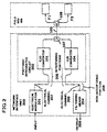
- FIG. 2 shows a block diagram of an exemplary optical communication system, utilizing a Network Interface Unit (NIU) 203 in accordance with the present invention.
- the NIU 203 includes (a) Electro-Optical (E/O) converter 101, (b) O/E converter 104, (c) filtering means 204, and (d) electrical modulator 201.
- E/O Electro-Optical
- O/E converter 104 O/E converter 104
- filtering means 204 filtering means 204
- electrical modulator 201 electrical modulator
- an input electrical signal is received at electrical modulator 201 which modulates the input electrical signal to a first predetermined frequency band to create a new electrical output signal.
- the new electrical output signal is then sent to E/O converter 101, via electrical channel 207, where it is converted to an optical signal centered at the exemplary frequency band F1, for transmission over optical waveguide 105.
- Optical signals to be received by NIU 203 which are transmitted from other NIUs in the system, are first received in frequency band F2 from optical transmission medium 105 and directional coupler 107 by O/E converter 104 and are converted into electrical output signals.
- the electrical output signal s are then transmitted over electrical channel 206 to filtering means 204.
- Interference in channel 206 is caused by the electrical signal in channel 207 in two ways. First, while traveling along portion 205 of electrical channel 206, the electrical signal in channel 206 picks up interference from the other electrical signal, previously discussed, which is traveling on portion 205 of electrical channel 207.
- Filtering means 204 is tuned to suppress substantially all energy in the first predetermined frequency band and, ideally, should be disposed anywhere along the non-interfering portion 208 of electrical channel 206. Therefore, filtering means 204 outputs an electrical signal on output 209 which is substantially free from interference caused by the signal on electrical path 207.
- PIC Photonic Integrated Circuit
- FIG. 3 shows an NIU 300 comprising similar components as those already discussed in FIG. 2.
- the NIU of FIG. 3 is suitable for use with the NIU of FIG. 2. More particularly, optical signals transmitted by E/O converter 101 of FIG. 2 are received by O/E converter 103 of FIG. 3 and are converted to an electrical signal, which is output by O/E converter 103 onto electrical channel 303. The frequency band of this output electrical signal will be determined by electrical modulator 201 of FIG. 2. Filtering means 301 then suppresses energy picked up from the electrical signal being used to drive E/O converter 102. Finally, electrical demodulator 302 demodulates the signal, thereby providing an output signal substantially free from interference.
- E/O converter 102 is used to convert an electrical signal to an optical signal for transmission to O/E converter 104 of FIG. 2.
- O/E converter 104 of FIG. 2 then converts the received optical signal to an electrical signal for transmission over electrical channel 206 as previously described.
- electrical modulator 201 could be replaced with an encoder, such as a spread spectrum encoder.
- the spread spectrum encoder would distribute the energy in the electrical input signal over a large bandwidth, thereby reducing the amount of energy present in the original bandwidth.
- filtering means 204 would be required to suppress all energy which was outside the original bandwidth, and thus, would suppress most of the energy from the interfering signal.
- Filtering means 204 may also include a spread spectrum decoder for decoding a spread spectrum signal being received by NIU 203. Analogous changes to other NIUs in the system, such as NIU 300 of FIG.
- any technique that distinguishes the energy in the two electrical signals and subsequently suppresses a larger fraction of the energy in the interfering signal than in the desired signal will suffice. It is also possible to include two modulators, one for each direction, and to convert the electrical signals into two different states rather than converting one of the electrical signals and leaving the second alone as was described previously herein.
- Filtering means 204 is understood to be any device capable of reducing the ratio of interfering energy to desired energy. Again, analogous changes to other NIUs in the system would have to be made. Both F1 and F2 could even be made equal to each other, as is the case in some systems.
- the electrical modulator of FIG. 2 could even be eliminated if the incoming electrical signal to the NIU was already in a state that was distinguishable from the electrical signal output from O/E converter 104.
Landscapes
- Engineering & Computer Science (AREA)
- Physics & Mathematics (AREA)
- Electromagnetism (AREA)
- Computer Networks & Wireless Communication (AREA)
- Signal Processing (AREA)
- Computer Security & Cryptography (AREA)
- Optical Communication System (AREA)
- Cable Transmission Systems, Equalization Of Radio And Reduction Of Echo (AREA)
Claims (10)
- Unité d'interface de réseau (UIR) destinée à former une interface entre un dispositif électrique et un réseau optique, cet UIR comportant:des première et seconde lignes (206, 207) de transmission électrique;des moyens (101) de conversion électro-optiques connectés à la première ligne de transmission électrique destinés à recevoir un premier signal électrique et à convertir le premier signal électrique en un premier signal optique pour être transmis au réseau optique;des moyens (104) de conversion optique-électriques destinés (a) à recevoir un second signal optique du réseau optique, (b) à convertir ce second signal optique en un second signal électrique, et (c) à transmettre le second signal électrique par l'intermédiaire de la seconde ligne de transmission électrique; caractérisée en ce queles lignes de transmission sont disposées de manière à obtenir un couplage électromagnétique notable entre elles; etle UIR comporte des moyens (204) connectés à la seconde ligne de transmission électrique destinée à augmenter un rapport de l'énergie dans le second signal électrique sur l'énergie qui est couplée électromagnétiquement de la première ligne de transmission électrique à la seconde ligne de transmission électrique.
- UIR suivant la revendication 1, dans lequel chacune des première et seconde lignes de transmission électriques comporte:
une première partie (205) et une deuxième partie (208), les premières parties étant positionnées les unes par rapport aux autres de manière qu'un signal électrique présent dans la première partie de l'une des lignes de transmission électriques est couplée par interférence à la première partie de l'autre des lignes de transmission électriques, et les secondes parties sont disposées les unes par rapport aux autres de sorte qu'un signal électrique présent dans la seconde partie de l'une des lignes de transmission électriques est sensiblement non couplé à l'autre ligne de transmission, et les moyens destinés à augmenter un rapport sont connectés à la seconde partie de la seconde ligne de transmission électrique. - UIR suivant la revendication 1 ou la revendication 2 qui comporte en outre des moyens de conversion électriques connectés à au moins l'une des lignes de transmission électriques pour convertir un signal électrique d'un premier état prédéterminé à un second état prédéterminé.
- UIR suivant la revendication 3, dans laquelle les moyens de conversion électriques comportent un modulateur destiné à recevoir un signal dans une première bande de fréquence prédéterminée et à convertir le signal à une seconde bande de fréquence prédéterminée.
- UIR suivant la revendication 3, dans laquelle les moyens de conversion électriques comportent un codeur destiné à recevoir le premier signal électrique et à coder le premier signal électrique en un signal codé suivant un code prédéterminé.
- UIR suivant l'une quelconque des revendications précédentes, dans laquelle les moyens de conversion électro-optiques et les moyens de conversion optique-électriques sont fabriqués en étant adjacents l'un à l'autre sur un circuit intégré photonique (PIC).
- UIR suivant l'une quelconque des revendications précédentes, connectée à un coupleur directionnel optique.
- Procédé pour obtenir une immunité contre les interférences dans deux canaux distincts spatialement, comportant les étapes qui consistent à:(a) convertir toute l'énergie dans un signal destiné à être transmis sur un premier de canaux distincts spatialement en un premier état prédéterminé, pour produire un signal électrique converti,(b)transmettre le signal électrique converti par le premier canal distinct spatialement,(c) augmenter, dans le second des canaux distincts spatialement, un rapport de l'énergie dans un second état prédéterminé qui se propage par le second des deux canaux distincts spatialement sur les interférences dues à l'énergie dans le premier état prédéterminé provenant du signal électrique converti couplé électromagnétiquement dans le second des canaux distincts spatialement.
- Procédé suivant la revendication 8, dans lequel à l'étape (a), le premier état prédéterminé est obtenu en décalant l'énergie dans une première bande de fréquence prédéterminée.
- Procédé suivant la revendication 8, dans lequel à l'étape (a), le premier état prédéterminé est obtenu en codant le signal électrique suivant un code prédéterminé.
Applications Claiming Priority (2)
| Application Number | Priority Date | Filing Date | Title |
|---|---|---|---|
| US449039 | 1989-12-12 | ||
| US07/449,039 US5005212A (en) | 1989-12-12 | 1989-12-12 | Interference suppression in optical communication systems |
Publications (3)
| Publication Number | Publication Date |
|---|---|
| EP0433023A2 EP0433023A2 (fr) | 1991-06-19 |
| EP0433023A3 EP0433023A3 (en) | 1992-05-13 |
| EP0433023B1 true EP0433023B1 (fr) | 1997-03-05 |
Family
ID=23782631
Family Applications (1)
| Application Number | Title | Priority Date | Filing Date |
|---|---|---|---|
| EP90313461A Expired - Lifetime EP0433023B1 (fr) | 1989-12-12 | 1990-12-11 | Suppression d'interférences améliorée dans des systèmes de communication optiques |
Country Status (5)
| Country | Link |
|---|---|
| US (1) | US5005212A (fr) |
| EP (1) | EP0433023B1 (fr) |
| JP (1) | JP2854146B2 (fr) |
| CA (1) | CA2031966C (fr) |
| DE (1) | DE69030064T2 (fr) |
Families Citing this family (10)
| Publication number | Priority date | Publication date | Assignee | Title |
|---|---|---|---|---|
| DE69114414T2 (de) * | 1990-08-27 | 1996-04-18 | Canon Kk | Optisches Kommunikationsnetz. |
| JPH053458A (ja) * | 1990-10-26 | 1993-01-08 | Nec Corp | 光双方向伝送方法と装置 |
| EP0509500A3 (en) * | 1991-04-19 | 1993-04-21 | Ascom Tech Ag | Device for bidirectional simultaneous transmission of digital information |
| FR2682239B1 (fr) * | 1991-10-04 | 1994-11-04 | Cit Alcatel | Systeme de transmission bidirectionnelle, notamment par fibre optique, avec une porteuse unique pour les deux sens de transmission. |
| FI100074B (fi) * | 1992-06-17 | 1997-09-15 | Nokia Telecommunications Oy | Menetelmä tilaajayhteyden toteuttamiseksi sekä tilaajaverkko |
| US5535968A (en) * | 1992-07-27 | 1996-07-16 | Union Switch & Signal Inc. | Vital railway signal link |
| US5661585A (en) * | 1995-02-27 | 1997-08-26 | Lucent Technologies Inc. | Passive optical network having amplified LED transmitters |
| US5623363A (en) * | 1995-02-27 | 1997-04-22 | Lucent Technologies Inc. | Semiconductor light source having a spectrally broad, high power optical output |
| US20050089326A1 (en) * | 2003-10-03 | 2005-04-28 | Zvi Regev | Cancellation of transmitted signal crosstalk in optical receivers of diplexer-based fiber optic transceivers |
| US7451384B2 (en) * | 2004-07-15 | 2008-11-11 | Honeywell International Inc. | Error recovery in asynchronous combinational logic circuits |
Family Cites Families (7)
| Publication number | Priority date | Publication date | Assignee | Title |
|---|---|---|---|---|
| JPS5784149A (en) * | 1980-11-14 | 1982-05-26 | Hitachi Ltd | Semiconductor integrated circuit device |
| DE3106682A1 (de) * | 1981-02-23 | 1982-09-09 | Siemens AG, 1000 Berlin und 8000 München | Nachrichtenuebertragungssystem fuer duplex-betrieb ueber eine lichtleitfaser |
| JPS5819878U (ja) * | 1981-07-31 | 1983-02-07 | 株式会社クボタ | 作業車の屋根板取付構造 |
| JPS60263590A (ja) * | 1984-06-11 | 1985-12-27 | Sumitomo Electric Ind Ltd | 画像信号伝送方式 |
| CA1235185A (fr) * | 1985-06-12 | 1988-04-12 | Northern Telecom Limited | Ligne de service a fibres optiques |
| JPH0191350U (fr) * | 1987-12-09 | 1989-06-15 | ||
| US4893300A (en) * | 1988-08-01 | 1990-01-09 | American Telephone And Telegraph Company | Technique for reducing distortion characteristics in fiber-optic links |
-
1989
- 1989-12-12 US US07/449,039 patent/US5005212A/en not_active Expired - Lifetime
-
1990
- 1990-12-11 CA CA002031966A patent/CA2031966C/fr not_active Expired - Fee Related
- 1990-12-11 DE DE69030064T patent/DE69030064T2/de not_active Expired - Fee Related
- 1990-12-11 EP EP90313461A patent/EP0433023B1/fr not_active Expired - Lifetime
- 1990-12-12 JP JP2410202A patent/JP2854146B2/ja not_active Expired - Fee Related
Also Published As
| Publication number | Publication date |
|---|---|
| DE69030064D1 (de) | 1997-04-10 |
| JPH04100332A (ja) | 1992-04-02 |
| DE69030064T2 (de) | 1997-08-07 |
| EP0433023A3 (en) | 1992-05-13 |
| CA2031966C (fr) | 1995-02-14 |
| EP0433023A2 (fr) | 1991-06-19 |
| JP2854146B2 (ja) | 1999-02-03 |
| US5005212A (en) | 1991-04-02 |
Similar Documents
| Publication | Publication Date | Title |
|---|---|---|
| US4761833A (en) | Optical fibre network | |
| US10848246B2 (en) | Method and system for an optical connection service interface | |
| JP3293565B2 (ja) | 光増幅中継器 | |
| US4957339A (en) | Optical communication system, particularly in the subscriber area | |
| EP0433023B1 (fr) | Suppression d'interférences améliorée dans des systèmes de communication optiques | |
| RU2138913C1 (ru) | Способ передачи сигналов в пассивной оптической системе дальней связи | |
| KR940009440B1 (ko) | 장거리 양방향 광섬유 통신링크 | |
| CN214480625U (zh) | 量子通信系统及其发送端和接收端 | |
| US5189544A (en) | Bidirectional light waveguide telecommunication system | |
| US4709414A (en) | Optical fiber order wire system | |
| CA1297950C (fr) | Systeme de communication optique, particulierement pour abonnes | |
| KR102060987B1 (ko) | 5g 통신용 광파 회로와 이를 이용한 단일 채널의 전이중 광통신 시스템 | |
| JPS6135031A (ja) | 双方向光通信方式 | |
| WO2002093221A2 (fr) | Dispositif et procede pour recevoir, traiter et emettre des signaux optiques et electriques, et procede de fabrication d'un tel dispositif | |
| AU623467B2 (en) | Optical transmission system | |
| JP3054167B2 (ja) | 双方向光伝送方式および光受信装置 | |
| JP3258038B2 (ja) | 光通信方式 | |
| JP3156345B2 (ja) | 双方向光伝送装置 | |
| JPS59216336A (ja) | 光伝送方式 | |
| CN121603107A (zh) | 一种单纤双向相干光模块和光通信设备与网络 | |
| Bell et al. | Communications: Coherent optical communication shows promise, the FCC continues on its path of deregulation, and satellite communications go high-frequency | |
| JPH0897772A (ja) | 光伝送装置 | |
| Stern et al. | Short-wavelength transmission on 1300 nm optimized single-mode fiber | |
| EP1056232A2 (fr) | Système de communication d'informations et procédé de transfert d'informations | |
| Williams et al. | Maximum utilisation of an existing optical trunk network |
Legal Events
| Date | Code | Title | Description |
|---|---|---|---|
| PUAI | Public reference made under article 153(3) epc to a published international application that has entered the european phase |
Free format text: ORIGINAL CODE: 0009012 |
|
| AK | Designated contracting states |
Kind code of ref document: A2 Designated state(s): DE GB |
|
| PUAL | Search report despatched |
Free format text: ORIGINAL CODE: 0009013 |
|
| AK | Designated contracting states |
Kind code of ref document: A3 Designated state(s): DE GB |
|
| 17P | Request for examination filed |
Effective date: 19921023 |
|
| RAP3 | Party data changed (applicant data changed or rights of an application transferred) |
Owner name: AT&T CORP. |
|
| 17Q | First examination report despatched |
Effective date: 19940921 |
|
| GRAG | Despatch of communication of intention to grant |
Free format text: ORIGINAL CODE: EPIDOS AGRA |
|
| GRAH | Despatch of communication of intention to grant a patent |
Free format text: ORIGINAL CODE: EPIDOS IGRA |
|
| GRAH | Despatch of communication of intention to grant a patent |
Free format text: ORIGINAL CODE: EPIDOS IGRA |
|
| GRAA | (expected) grant |
Free format text: ORIGINAL CODE: 0009210 |
|
| AK | Designated contracting states |
Kind code of ref document: B1 Designated state(s): DE GB |
|
| REF | Corresponds to: |
Ref document number: 69030064 Country of ref document: DE Date of ref document: 19970410 |
|
| PLBE | No opposition filed within time limit |
Free format text: ORIGINAL CODE: 0009261 |
|
| STAA | Information on the status of an ep patent application or granted ep patent |
Free format text: STATUS: NO OPPOSITION FILED WITHIN TIME LIMIT |
|
| 26N | No opposition filed | ||
| REG | Reference to a national code |
Ref country code: GB Ref legal event code: IF02 |
|
| PGFP | Annual fee paid to national office [announced via postgrant information from national office to epo] |
Ref country code: GB Payment date: 20021126 Year of fee payment: 13 |
|
| PGFP | Annual fee paid to national office [announced via postgrant information from national office to epo] |
Ref country code: DE Payment date: 20021205 Year of fee payment: 13 |
|
| PG25 | Lapsed in a contracting state [announced via postgrant information from national office to epo] |
Ref country code: GB Free format text: LAPSE BECAUSE OF NON-PAYMENT OF DUE FEES Effective date: 20031211 |
|
| PG25 | Lapsed in a contracting state [announced via postgrant information from national office to epo] |
Ref country code: DE Free format text: LAPSE BECAUSE OF NON-PAYMENT OF DUE FEES Effective date: 20040701 |
|
| GBPC | Gb: european patent ceased through non-payment of renewal fee |
Effective date: 20031211 |