EP0433087A2 - Multiplex-Lumineszenzdiode-Druckkopf - Google Patents
Multiplex-Lumineszenzdiode-Druckkopf Download PDFInfo
- Publication number
- EP0433087A2 EP0433087A2 EP90313677A EP90313677A EP0433087A2 EP 0433087 A2 EP0433087 A2 EP 0433087A2 EP 90313677 A EP90313677 A EP 90313677A EP 90313677 A EP90313677 A EP 90313677A EP 0433087 A2 EP0433087 A2 EP 0433087A2
- Authority
- EP
- European Patent Office
- Prior art keywords
- light emitting
- die
- emitting diode
- data
- dice
- Prior art date
- Legal status (The legal status is an assumption and is not a legal conclusion. Google has not performed a legal analysis and makes no representation as to the accuracy of the status listed.)
- Withdrawn
Links
Images
Classifications
-
- G—PHYSICS
- G06—COMPUTING OR CALCULATING; COUNTING
- G06K—GRAPHICAL DATA READING; PRESENTATION OF DATA; RECORD CARRIERS; HANDLING RECORD CARRIERS
- G06K15/00—Arrangements for producing a permanent visual presentation of the output data, e.g. computer output printers
- G06K15/02—Arrangements for producing a permanent visual presentation of the output data, e.g. computer output printers using printers
- G06K15/12—Arrangements for producing a permanent visual presentation of the output data, e.g. computer output printers using printers by photographic printing, e.g. by laser printers
- G06K15/1238—Arrangements for producing a permanent visual presentation of the output data, e.g. computer output printers using printers by photographic printing, e.g. by laser printers simultaneously exposing more than one point
- G06K15/1242—Arrangements for producing a permanent visual presentation of the output data, e.g. computer output printers using printers by photographic printing, e.g. by laser printers simultaneously exposing more than one point on one main scanning line
- G06K15/1247—Arrangements for producing a permanent visual presentation of the output data, e.g. computer output printers using printers by photographic printing, e.g. by laser printers simultaneously exposing more than one point on one main scanning line using an array of light sources, e.g. a linear array
Definitions
- non-impact electrophotographic printers for text and graphics.
- an electrostatic charge is formed on a photo-receptive surface of a moving drum or belt, and selected areas of the surface are discharged by exposure to light.
- a printing toner is applied to the drum and adheres to the areas having an electrostatic charge and does not adhere to the discharged areas. This method is referred to a "writing white”.
- the toner is then transferred to a sheet of plain paper and is heat- and/or pressure-fused to the paper.
- characters, lines and other images may be produced on the paper.
- Other types of printers may use similar exposure, such as "writing black” which is essentially the reverse of the charging and discharging just mentioned, or for exposing photographic or other photosensitive materials.
- One type of nonimpact printer employs an array of light emitting diodes (commonly referred to herein as LEDs) for exposing the photoreceptive surface.
- LEDs light emitting diodes
- a row, or several closely spaced rows, of minute LEDs are positioned near an elongated lens array so that their images are arrayed across the surface to be illuminated.
- they are selectively activated to either emit light or not, thereby exposing or not exposing, the photoreceptive surface in a pattern corresponding to the LEDs activated.
- the light output of each LED is controlled to obtained the appropriate density of image.
- an adjustable constant current source for each LED junction is used to obtain a desired light output as a function of current. LEDs are switched on or off as appropriate for the data being printed. If used in a gray scale printer, the total exposure on a pixel by an LED depends on the time interval when it is turned on and on the current through the LED. Data for driving the individual LEDs across a printhead is, therefore, often in the form of pulse width modulation, but may also be in the form of current modulation.
- Light emitting diodes for print heads are formed on wafers of gallium arsenide or the like, suitably doped to conduct current and emit light. Long arrays of LEDs are formed on a wafer which is cut into separated dice, each having an array of LEDs. A row of such dice are assembled end-to-end to form a print head array.
- each integrated circuit chip has adjustable means for setting a reference voltage for the current sources.
- each current source comprises a field effect transistor (FET) gated by the reference voltage.
- FET field effect transistor
- each current source also includes a data FET in series with the constant current FET which, in response to a data signal at its gate, interconnects the constant current FET to an individual LED on the chip connected to that integrated circuit.
- each constant current driver for an LED is on only a small fraction of the time.
- This invention therefore, employs time multiplexing so that each current source can be shared among many LEDs, thereby resulting in very substantial cost reductions for an LED printhead.
- a multiplexed set of current sources for a light emitting diode print head having a row of LED dice, each die having a row of LEDs.
- Each LED die substrate forms a common cathode for the LEDs on that die.
- a switch selectively connects the substrate of each die to ground, and at the same time, data for a selected die is applied in parallel to the anodes of corresponding LEDs on all the dice for enabling the LEDs on only the die having its substrate switched to ground.
- a time multiplex driver for a plurality of dice comprising a plurality of current driver FETs connected to a common gate bias voltage, and a plurality of data FETs, each data FET being in series with a current driver FET.
- Each data FET is connected to the anodes of the corresponding light emitting diodes on all of the dice, respectively.
- FET or bipolar switches selectively connect the substrate of each die to ground.
- Means are provided for applying data for a selected die to the anodes of corresponding LEDs on all the dies and at the same time selectively connecting the substrate of the selected die to ground. This enables only the light emitting diodes on the selected die for illuminating the desired pixels.
- the exposure data are loaded into a shift register and latched.
- a block of the latched pixel data and a block of latched current drive data for enabling the LEDs on a selected die are applied to the respective data FETs at the same time the switch for the selected die is closed.
- Transmission gates may be used for connecting the selected block of the shift register to the data FETs.
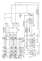
- An exemplary LED print head has a row of light emitting diode (LED) dice 10 placed end-to-end to stretch across the width of a photoreceptive surface. Each die has a row of LEDs 11 n along its length.
- LED light emitting diode
- each die has 64 LEDs along its length. Eight such LED dice 101, 102 . . . 108 are in a row for control by circuits on one integrated circuit chip. It will be recognized that this is merely exemplary and there are many other arrangements to which this invention may be applicable. For example, the odd numbered LEDs on a die may be controlled by circuits on one integrated circuit chip and the even numbered LEDs on the die may be controlled by circuits on another integrated circuit chip. clearly, other numbers of LEDs and/or dice may be involved. The LEDs are also assumed to be on dice where the cathodes of all of the LEDs are common and separate electrical connections are made to the anodes of each LED. Other types of LEDs (e.g. AlGaAs) may have common connections for the anodes and individual connections for the cathodes. Reference to cathodes herein is a matter of convenience, and it will be understood that the reverse electrical connection is included as equivalent.
- AlGaAs AlGaAs
- the multiplexed current supply for the LED dice is on a silicon integrated circuit chip which may be adjacent to the row of LED dice.
- the integrated circuit chip is not separately identified in the drawing, but includes essentially everything in the drawing except the LED dice and some connections.
- the integrated circuit chip may also included additional circuit features, such as a reference voltage source, data processing gates and error compensation features.
- the integrated circuit includes a plurality of LED current sources corresponding to the number of LEDs on an LED die, thus, in the exemplary embodiment there are 64 current sources.
- Each current source comprises a p-channel output driver field effect transistor (FET) 13.
- a chip reference voltage V r is connected to the gate of each of the plurality of similar p-channel output driver FETs 131, 132 . . . 1364, which provide current for corresponding light emitting diodes 111, 112 . . . 1164 on respective dice.
- the current for each driver is substantially identical. These can be thought of as current mirrors with the same current flow as in a reference constant current cell (not shown).
- the light output, rise time and the like is substantially identical for all of the LEDs.
- the current from each driver FET, and the respective rise and fall time, for each LED is substantially independent of the number of LEDs enabled.
- Each of the output driver FETs 13 is in series with a p-channel data FET 151, 152 . . . 1564.
- the data FETs 15 act as switches in response to presence or absence of a data signal applied to the gate of the respective data FET.
- each data FET is applied to the anode of the corresponding LED on each of the eight LED dice 101, 102...108. That is, the output of the first data FET is connected in parallel to the anodes of the corresponding LED's.
- the output of the first data FET 151 is applied in parallel to the corresponding LED 111 on each of the eight dice.
- the output of the second data FET 152 is connected in parallel to the corresponding LED's 112, on all of the eight dice, and so on across the full plurality of current sources and LEDs.
- Data for switching the data FETs is loaded serially into eight shift registers 19, each register having 64 bits.
- the shift registers can also be considered as a 512 bit shift register divided into eight blocks of 64 bits each.
- the data for 512 LEDs has been loaded into the shift register, the data are latched and the register can then be used to receive the next line of 512 bits of data.
- Data for each LED determines whether an LED is lighted during printing of a line.
- the latched data in each bit of the register may be sampled with a transmission gate 21.
- the control input to all of the transmission gates in each of the eight shift registers are connected in parallel to a respective output of a decoder/counter 23.
- all of the control inputs for the transmission gates for the first shift register 191 are connected in parallel to the l output of the decoder/counter.
- all of the control inputs for the transmission gates connected to the second shift register 192 are connected in parallel to the 2 output of the decoder/counter, and so on for all eight shift registers.
- the data latch signals are used to increment the counter 23 and transmission gates need not be used.
- Other loading and reading arrangements will be apparent. For example, one may load data for dice 1, 9, 17, 25, etc. and when these dice are turned on, one may load data for dice 2, 10, 18, 26, etc. Such multiplexing arrangements can be provided in the data source circuitry.
- the output terminals of the first transmission gates in all of the eight shift registers are connected in parallel to the gate of the first data FET 151.
- the output terminals of all of the transmission gates for the second bit in each of the eight registers are connected in parallel to the gate of the second data FET 152, and so on across the array until the last transmission gates for all the registers are connected to the last data FET 1564.
- the respective outputs of the decoder/counter 23 are also applied to the gates of the cathode switching transistors 17.
- the 1 output of the decoder/counter is connected to the gate of the first cathode switching transistor 171 which is connected to the substrate of the first LED die 101.
- the rest of the eight outputs of the decoder/counter are similarly connected to the gates of the other cathode switching transistors 17 for selectively connecting the substrate of each die to ground.
- the LEDs on a die are enabled according to the data latched in a respective shift register in response to clock counting in the decoder/counter.
- the signal applied to the control inputs of the transmission gates in the first register 191 applies the 64 signals latched in the first shift register to the 64 data FETs 15, respectively.
- the data FET conducts so that current is available from the respective current source 13 to all of the corresponding LEDs on the eight dice.
- the 1 output of the decoder/counter is also applied to the gate of the first cathode switching transistor 171, thereby permitting the LEDs on the first die 101 to conduct and illuminate the corresponding pixels.
- each shift register and corresponding cathode switching transistor are enabled in turn for sequentially enabling the LEDs on each of the eight LED dice in turn.
- An LED printhead exposes the photoreceptive surface of a drum or belt in a series of rows of dots extending across the drum.
- a separate line of data is used for each line of illumination by the LEDs.
- the decoder/counter may scan all the shift registers in the time required to illuminate one line on the drum. On the other hand, it may be desirable to count two or four times across the decoder/counter during the time one line is exposed, thereby integrating the illumination of smaller areas on the moving drum in response to repeated shorter pulses of current on the LEDs. Other sequences of multiplexing may be used as well.
- the cathode switching transistors 17 carry appreciable current since connected in parallel to the cathodes of numerous LEDs.
- they may preferably be located on a separate chip so that bipolar transistors or large area vertical MOSFETs may be used, and that heat generated can be dissipated separately from the chip with other integrated circuits and thereby minimize heating of the balance of the electronics.
- this example of multiplexing reduces the number of current sources from 512 to only 64.
- the two FETs 13, 15 in each of these sources are relatively high-current devices (as much as 100 milliamps).
- the greatest savings come about from the substantial reduction in the number of current drivers. The extent of such savings will of course depend on the number of chips and LEDs multiplexed.
- Parallel connections can be made using a variety of fine line circuit techniques, such as TAB bonding film, fine lines deposited on a ceramic substrate, a ceramic filled epoxy or fiber glass substrate with printed lines, etc., or a fine line metal on glass system with the LEDs inverted for illumination through the glass substrate.
- fine line circuit techniques such as TAB bonding film, fine lines deposited on a ceramic substrate, a ceramic filled epoxy or fiber glass substrate with printed lines, etc., or a fine line metal on glass system with the LEDs inverted for illumination through the glass substrate.
- conventional wire bonding may be used between metal connection lines on the substrate and LED connection pads as is conventional.
- multiplexed current source for an LED print head has been described and illustrated herein, many modifications and variations will be apparent to those skilled in the art.
- FETs are particularly suitable for switching as described herein, equivalent devices may be substituted.
- p-channel FETs are used in the drivers, the circuits can be modified to use n-channel FETs , MOSFETs, or bipolar transistors to accomplish the same purposes.
- discrete components may be used. Either multiple or single transistor transmission gates or tri-state logic may be used for applying data from the registers to the data FETs.
Landscapes
- Physics & Mathematics (AREA)
- Engineering & Computer Science (AREA)
- Optics & Photonics (AREA)
- General Engineering & Computer Science (AREA)
- General Physics & Mathematics (AREA)
- Theoretical Computer Science (AREA)
- Printers Or Recording Devices Using Electromagnetic And Radiation Means (AREA)
Applications Claiming Priority (2)
| Application Number | Priority Date | Filing Date | Title |
|---|---|---|---|
| US07/451,319 US4998119A (en) | 1989-12-15 | 1989-12-15 | Multiplexed light emitting diode printhead |
| US451319 | 1995-05-26 |
Publications (2)
| Publication Number | Publication Date |
|---|---|
| EP0433087A2 true EP0433087A2 (de) | 1991-06-19 |
| EP0433087A3 EP0433087A3 (en) | 1992-03-04 |
Family
ID=23791742
Family Applications (1)
| Application Number | Title | Priority Date | Filing Date |
|---|---|---|---|
| EP19900313677 Withdrawn EP0433087A3 (en) | 1989-12-15 | 1990-12-14 | Multiplexed light emitting diode printhead |
Country Status (2)
| Country | Link |
|---|---|
| US (1) | US4998119A (de) |
| EP (1) | EP0433087A3 (de) |
Cited By (1)
| Publication number | Priority date | Publication date | Assignee | Title |
|---|---|---|---|---|
| WO1994004994A1 (de) * | 1992-08-24 | 1994-03-03 | Siemens Aktiengesellschaft | Anordnung zur gleichzeitigen steuerung von einer vielzahl von leuchtdioden |
Families Citing this family (7)
| Publication number | Priority date | Publication date | Assignee | Title |
|---|---|---|---|---|
| US5163760A (en) * | 1991-11-29 | 1992-11-17 | Eastman Kodak Company | Method and apparatus for driving a thermal head to reduce parasitic resistance effects |
| JPH07223337A (ja) * | 1994-01-14 | 1995-08-22 | Xerox Corp | デジタルプリンター、及びledプリントバーにおけるled画素の光電変換効率の補正方法 |
| US7385574B1 (en) | 1995-12-29 | 2008-06-10 | Cree, Inc. | True color flat panel display module |
| JPH10235935A (ja) * | 1997-02-27 | 1998-09-08 | Oki Data:Kk | ドライバicとledプリントヘッド |
| JP4086343B2 (ja) * | 1997-06-30 | 2008-05-14 | 沖電気工業株式会社 | プリントヘッド |
| US7561118B2 (en) * | 2004-11-12 | 2009-07-14 | Hewlett-Packard Development Company, L.P. | Multiplexing |
| US8576183B2 (en) * | 2009-09-23 | 2013-11-05 | Infineon Technologies Ag | Devices and methods for controlling both LED and touch sense elements via a single IC package pin |
Family Cites Families (4)
| Publication number | Priority date | Publication date | Assignee | Title |
|---|---|---|---|---|
| EP0026452A3 (de) * | 1979-09-26 | 1981-07-22 | Siemens Aktiengesellschaft | Vorrichtung zur Erzeugung von Ladungsbildern auf einem fotoleitenden Bildträger |
| US4427275A (en) * | 1982-07-22 | 1984-01-24 | Pitney Bowes Inc. | Xerographic electronic printer |
| US4689694A (en) * | 1983-01-12 | 1987-08-25 | Canon Kabushiki Kaisha | Image recording apparatus utilizing linearly arranged recording elements |
| JPH02274570A (ja) * | 1989-04-17 | 1990-11-08 | Tokyo Electric Co Ltd | 端面発光型elプリンタ及びその印刷方法 |
-
1989
- 1989-12-15 US US07/451,319 patent/US4998119A/en not_active Expired - Lifetime
-
1990
- 1990-12-14 EP EP19900313677 patent/EP0433087A3/en not_active Withdrawn
Cited By (1)
| Publication number | Priority date | Publication date | Assignee | Title |
|---|---|---|---|---|
| WO1994004994A1 (de) * | 1992-08-24 | 1994-03-03 | Siemens Aktiengesellschaft | Anordnung zur gleichzeitigen steuerung von einer vielzahl von leuchtdioden |
Also Published As
| Publication number | Publication date |
|---|---|
| US4998119A (en) | 1991-03-05 |
| EP0433087A3 (en) | 1992-03-04 |
Similar Documents
| Publication | Publication Date | Title |
|---|---|---|
| US4734714A (en) | Optical print head with LED diode array | |
| US5138310A (en) | Light-emitting element array driver circuit | |
| US5815025A (en) | Intensity controlling circuit device for LED-array head having a plurality of LED-array chips | |
| US8258723B2 (en) | Light-emitting element array, driving device, and image forming apparatus | |
| EP0936509B1 (de) | Treiberschaltung und LED-Kopf mit konstanter Einschaltzeit | |
| EP0419255A2 (de) | Verfahren und Vorrichtung zur Kontrolle der sichtbaren Gleichförmigkeit von LED-Druckköpfen | |
| JP3308801B2 (ja) | 記録素子アレイ | |
| JP2816147B2 (ja) | 発光ダイオードアレイ用駆動回路 | |
| CN101734021B (zh) | 发光元件头、图像形成装置以及信号供给方法 | |
| US6172701B1 (en) | Light emitting element array chip, light emitting element array drive IC and print head | |
| US5892532A (en) | Non-impact printer and a print head thereof | |
| US4998119A (en) | Multiplexed light emitting diode printhead | |
| CN102244071B (zh) | 发光装置及阵列单元、打印头、成像设备及发光控制方法 | |
| US6683638B2 (en) | Print head and image forming apparatus using multiplexed compensation data | |
| US5734406A (en) | Driver IC, a print head having the driver IC and a printer including the print head | |
| WO1992000196A1 (en) | L.e.d. array printer | |
| CN102709305B (zh) | 发光芯片、打印头和图像形成设备 | |
| US7330204B2 (en) | Self-scanning light-emitting element array and driving method of the same | |
| US5166702A (en) | LED printhead with improved current mirror driver and driver chip therefor | |
| US6750895B1 (en) | Optical printer head with integrated drive circuitry | |
| US6022155A (en) | Driver IC and print head | |
| US6351278B1 (en) | Circuit for controlling current for driving printing dot array | |
| JP2001284653A (ja) | 発光素子アレイ | |
| US8587628B2 (en) | Driver apparatus, print head, and image forming apparatus | |
| US7242416B2 (en) | Optical head |
Legal Events
| Date | Code | Title | Description |
|---|---|---|---|
| PUAI | Public reference made under article 153(3) epc to a published international application that has entered the european phase |
Free format text: ORIGINAL CODE: 0009012 |
|
| AK | Designated contracting states |
Kind code of ref document: A2 Designated state(s): DE FR GB |
|
| PUAL | Search report despatched |
Free format text: ORIGINAL CODE: 0009013 |
|
| AK | Designated contracting states |
Kind code of ref document: A3 Designated state(s): DE FR GB |
|
| STAA | Information on the status of an ep patent application or granted ep patent |
Free format text: STATUS: THE APPLICATION IS DEEMED TO BE WITHDRAWN |
|
| 18D | Application deemed to be withdrawn |
Effective date: 19920905 |