EP0433142A1 - Multiprozessor-Datenverarbeitungssystem mit einem rekonfigurierbaren aktiven Bus - Google Patents
Multiprozessor-Datenverarbeitungssystem mit einem rekonfigurierbaren aktiven Bus Download PDFInfo
- Publication number
- EP0433142A1 EP0433142A1 EP90403481A EP90403481A EP0433142A1 EP 0433142 A1 EP0433142 A1 EP 0433142A1 EP 90403481 A EP90403481 A EP 90403481A EP 90403481 A EP90403481 A EP 90403481A EP 0433142 A1 EP0433142 A1 EP 0433142A1
- Authority
- EP
- European Patent Office
- Prior art keywords
- data processing
- data
- bus
- input
- module
- Prior art date
- Legal status (The legal status is an assumption and is not a legal conclusion. Google has not performed a legal analysis and makes no representation as to the accuracy of the status listed.)
- Ceased
Links
Images
Classifications
-
- G—PHYSICS
- G06—COMPUTING OR CALCULATING; COUNTING
- G06F—ELECTRIC DIGITAL DATA PROCESSING
- G06F15/00—Digital computers in general; Data processing equipment in general
- G06F15/16—Combinations of two or more digital computers each having at least an arithmetic unit, a program unit and a register, e.g. for a simultaneous processing of several programs
- G06F15/163—Interprocessor communication
- G06F15/173—Interprocessor communication using an interconnection network, e.g. matrix, shuffle, pyramid, star, snowflake
- G06F15/17337—Direct connection machines, e.g. completely connected computers, point to point communication networks
- G06F15/17343—Direct connection machines, e.g. completely connected computers, point to point communication networks wherein the interconnection is dynamically configurable, e.g. having loosely coupled nearest neighbor architecture
Definitions
- the field of the invention is that of multiprocessor data processing systems.
- the invention relates to a multiprocessor data processing system with a reconfigurable active bus.
- processor-to-processor connection networks as in hypercubes, "Tansputers”, systolic arrays.
- the interprocessor communication channel typically consists of a parallel bus, the data transfers taking place from the storage unit associated with a processor to the storage unit associated with a remote processor.
- Interprocessor data transfers can consist of a movement of large blocks of data but also in a movement of a multiplicity of small blocks.
- patent US-0 234182 discloses the use of a dual-access memory enabling the data to be transferred to be transferred via the communication channel to be stored in a first memory area while the communicating processor continues processing in association with a second memory area.
- multiprocessor machines with parallel processing resides in their irregularity of computing power with respect to the various fields of application.
- multiprocessor machines generally include high-performance but expensive processors.
- Massively parallel machines include a multiplicity of modest processors.
- the fields of application of these machines being most often heterogeneous, as well as the algorithms used, in particular in terms of arithmetic calculations, we therefore obtain non-regular computing power for one or the other of these two categories of machines.
- the structural rigidity of current multiprocessor data processing systems is completely unsuited to the considerable number of algorithms which must be implemented where only the number of calculation units is a determining factor and it is advantageous to have '' a system intrinsically combining the qualities of multiprocessor machines and parallel processing machines.
- the multiprocessor data processing system disclosed in the patent cited above includes an inert interprocessor bus which does not provide any improvement in the computing power of the entire system.
- this type of known system has temporally fixed characteristics and does not allow flexible interprocessor coupling.
- the objective of the invention is to solve these various problems.
- a first objective of the invention is to provide a multiprocessor data processing system with reconfigurable active bus making it possible to distribute between the processors and the active bus, classes of data processing algorithms so as to constitute a modular system having two distinct layers, a first layer consisting of cascaded data processing units of the type with multiple instructions, multiple data, for example, inducing medium grain parallelism and a second layer consisting of circuits controlled by data flows integrating functions communication, synchronization and parallel fine grain calculations, this layer forming the reconfigurable active bus.
- Another objective of the invention is to provide a reconfigurable active bus data processing system, in which the communication protocol is managed directly at the level of the communication channel, that is to say at the level of the bus.
- Another object of the invention is to provide a reconfigurable active bus data processing system in which the data processing functions managed by the processors of the system have been decoupled from the functions for managing the interprocessor communication protocol managed by the active bus enabling very high communication speed and computing power in parallel.
- a reconfigurable active bus multiprocessor data processing system comprising at least two interconnectable modules connected by a module interconnect bus, an interconnectable module comprising a processing unit. data, an addressable storage unit and controllable by the data processing unit via a system bus,
- said module further comprises a configurable and reconfigurable base constituting a node of the module interconnection bus, said base comprising a first input / output interface means connected to the system bus and operating with the data processing unit and the storage unit, second input / output interface means connected to the module interconnection bus for operating respectively with the second input / output interface means of the adjacent module, means for synthesizing a plurality of operating circuits receiving input data from said interface means and restoring resulting data to said interface means, means for creating and switching data paths between said input / output interface means, said base being configured and reconfigured by the unit data processing by means of configuration information via the system bus.
- the means of synthesis of operating circuits in the base allow a distribution of the internal computing power of the module between the data processing unit or processor and the base or node of the communication bus.
- the input / output interface means in association with the means for creating and switching configurable data paths allow flexible routing of data on the bus regardless of the activity of the data processing unit.
- As the base is configurable or reconfigurable by loading configuration information, it behaves like an intelligent node for intermodule communication. This results in a significant gain in terms of control, test or distribution operations. data previously managed by the processors of the system.
- the storage unit comprises a first storage area and a second storage area, means for transferring data between the two storage areas, the first storage area and the transfer means being addressable and controllable via the system bus by the data processing unit, the second storage area and the transfer means being accessible and controllable via a communication channel by the base further comprising a third input interface means / output operating with the means for creating and switching data paths.
- a real loopback is made between the data processing unit, the base and the storage unit. In this way we obtain an overlap of the tasks carried out at the level of the data processing unit and the base.
- the dual access partitioned memory allows gain in bandwidth and control operations.
- the loopback ensures data dissemination through the internal channels of the module without interrupting the local processing in progress.
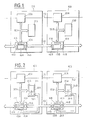
- FIG. 1 schematically represents a reconfigurable active bus multiprocessor data processing system comprising interconnectable modules according to the invention
- FIG. 2 schematically shows the multiprocessor bus data processing system reconfigurable asset according to the invention in which each module comprises a dual-access memory.
- the multiprocessor data processing system illustrated in FIG. 1, comprises two interconnectable modules 10A, 10B.
- the first module typically comprises a data processing unit 20A or processor, a data storage and program unit 30A connected to the unit 20A by a system bus 50A comprising in known manner, address and control so that the data processing unit is able to address and control the storage unit.
- the second module 10B comprises a data processing unit 20B connected to a data and program storage unit 30B via a system bus 50B.
- the two data processing units 20A, 20B are cascaded and connected by a communication network 70 so as to ensure weak coupling between them.
- provision may be made for the cascade connection of other data processing units, so as to produce a system comprising a plurality of processors.
- the processors can be compared to Transputers inducing a parallel with medium grain.
- the module 10A also comprises a base 40A placed at a node of an intermodule interconnection bus 60. It is the same for the module 10B and we will describe below only the module 10A.
- the base 40A is based on the technology of an array of logic cells commonly called LCA (Logic Cells Array).
- LCA contains three types of elements; an input / output block perimeter, a central table of configurable logic blocks and block interconnection resources.
- the configuration of the three types of elements is determined by configuration information previously loaded in the LCA, which is toggled for this purpose in a configuration mode.
- Such circuits are commercially available under the reference AMD 3090 for example.
- a plurality of input / output blocks of the LCA are used to constitute a first parallel input / output interface 41A preferably comprising 32 data input / output blocks and 4 input / output blocks assigned to control lines, the first parallel input / output interface 41A being directly connected to the system bus 50A so that the base 40A can be addressable and controllable via the system bus 50A by the data processing unit 20A.
- a plurality of other input / output blocks of the LCA are similarly used to constitute two second parallel input / output interface means 42A, 44A for example twice 36 blocks for connecting at least one adjacent module 10B to the module 10A via the module interconnection bus 60 and operate respectively with the second input / output interface means 42B, 44B associated with the second adjacent module.
- the module interconnection bus 60 has 32 data transmission lines and 4 control lines. However, provision may be made for different organization and use of the different lines of the interconnection bus depending on the configuration of the input / output blocks of the LCA.
- the central table of configurable logic blocks allows the synthesis of operating circuits 43A for example of logical or arithmetic functions defined by the loading of internal LCA scan tables.
- the operating circuits implement algorithms for parallel processing.
- the routing of data through the synthesized operating circuits and between the various input / output interface means 41A, 42A, 44A is obtained by the configuration of the interconnection resources 43A of the LCA allowing the creation or modification of links between the blocks LCA logic.
- the operating circuits are controlled by the data flow coming from the input interface means 41A, 42A, 44A and the results of the processing are routed to the output interface means 41A, 42A, 44A so that the base 40A constitutes in itself a pseudo processor has fine grain parallel data processing.
- the routing of data from and to the input / output interface means 41A, 42A, 44A and the constitution of the operating circuits are defined by information on the configuration of the base 40A.
- the configuration information previously stored in the storage unit 30A is loaded into the base 40A in a known manner via the system bus 50A on the initiative of the data processing unit 20A and is modified in the same way to reconfigure the base 40A depending on the processing or the data switches to be performed.
- the multiprocessor data processing system is initialized, it will be possible to load all of the configuration information respectively into the storage units 30A, 30B associated with each module 10A, 10B from an external site via the interprocessor network 70.
- each processing unit 20A can configure its associated base 40A to, firstly logically establish the data transfer paths via the interconnection bus of modules 60, and secondly share, synthesize the operating circuits parallel operation or not in order to deport part of their computing power
- the base 40A thus plays the role of an accelerator of the data processing unit 20A and makes it possible to flexibly establish a path for the dissemination of global data to all of the data processing units of the system.
- the base 40A requisitions access from the system bus 50A and consequently affects the processing capacity of the unit data processing unit 20A which shares the system bus 50A. It is therefore advantageous to directly supply the synthesized operating circuits of the base 40A without requisitioning the system bus 50A.
- the storage unit 30A is a video memory (VRAM) of the TMS44 C251 type from Texas Instruments and comprises a first storage area 31A, a second storage area 32A and means 33A data transfer characteristic of video RAM allowing data exchange between the two storage areas.
- VRAM video memory
- the first storage area 31A consists of a RAM area associated with a parallel input / output port accessed and controlled by the data processing unit 20A, via the system bus 50A.
- the second storage area 32A consists of an assembly of serial registers associated with a serial input / output port accessed and controlled by the base 40A via a communication channel 75A connecting the input / output port associated with the second storage area 32A to a third input / output interface means 45A corresponding to the base 40A constituted by a plurality of input / output blocks of the LCA.
- the base 40A can use a request line to sequentially read the data stored in the serial input / output port of the RAM video or to store data there.
- the data processing unit 20A via the system bus 50A controls, in a known manner, the data transfer means 33A to transfer data stored in the first memory area 31A to the second memory area 32A to supply the base 40A and vice versa the base 40A controls the data transfer means 33A via the communication channel 75A, to transfer data stored in the second memory area 32A to the first memory area 31A to supply the data processing unit 20A.
- the data processing unit 20A transfers in parallel from the first storage area 31A of the unit memory 30A, four operands to the first interface means configured at input 41A of the base 40A.
- the means for synthesizing operating circuits 43A being configured to perform four operations in parallel, the four operands are respectively sent to the synthesized operating circuits 43A which can simultaneously deliver four results to the second interface means configured at output 44A of the base 40A, which transfer them to the second interface means configured at input 42B of the base 40B of the module 10B.
- the base 40B previously configured to establish data communication links between the second input interface means 42B and the third interface means configured at output 45B transfers the resulting data to the second storage area 32B of the storage unit 30B of module 10B.
- the base 40B causes the transfer of data from the second zone of storage 32B to the first storage area 31B.
- the data processing unit 20B then accesses the data loaded in the first storage area 32B to complete the processing.
- the module interconnection bus according to the invention is both a processing channel and a communication channel allowing the establishment of a parallelism which can be very fine or of distributed algorithms.
- the system according to the invention can be considered as a layer of conventional processors (MIMD) controlling a layer of combinational or sequential circuits reconfigurable according to the needs of the application.
- MIMD conventional processors
- the reconfigurable active bus multiprocessor data processing system has the advantage of being easily extensible. By interconnecting a plurality of modules according to the invention, it is easy, for example, to implement algorithms for broadcasting messages via the interconnection bus or to configure the base of each module as a crossbar as in systolic machines.
Landscapes
- Engineering & Computer Science (AREA)
- Computer Hardware Design (AREA)
- Physics & Mathematics (AREA)
- Theoretical Computer Science (AREA)
- Mathematical Physics (AREA)
- Software Systems (AREA)
- General Engineering & Computer Science (AREA)
- General Physics & Mathematics (AREA)
- Multi Processors (AREA)
Applications Claiming Priority (2)
| Application Number | Priority Date | Filing Date | Title |
|---|---|---|---|
| FR8916334A FR2655750B1 (fr) | 1989-12-11 | 1989-12-11 | Systeme de traitement de donnees multiprocesseur a bus actif reconfigurable. |
| FR8916334 | 1989-12-11 |
Publications (1)
| Publication Number | Publication Date |
|---|---|
| EP0433142A1 true EP0433142A1 (de) | 1991-06-19 |
Family
ID=9388351
Family Applications (1)
| Application Number | Title | Priority Date | Filing Date |
|---|---|---|---|
| EP90403481A Ceased EP0433142A1 (de) | 1989-12-11 | 1990-12-06 | Multiprozessor-Datenverarbeitungssystem mit einem rekonfigurierbaren aktiven Bus |
Country Status (2)
| Country | Link |
|---|---|
| EP (1) | EP0433142A1 (de) |
| FR (1) | FR2655750B1 (de) |
Cited By (2)
| Publication number | Priority date | Publication date | Assignee | Title |
|---|---|---|---|---|
| US5465375A (en) * | 1992-01-14 | 1995-11-07 | France Telecom | Multiprocessor system with cascaded modules combining processors through a programmable logic cell array |
| WO1996041274A1 (en) * | 1995-06-07 | 1996-12-19 | Advanced Micro Devices, Inc. | Dynamically reconfigurable data bus |
Citations (2)
| Publication number | Priority date | Publication date | Assignee | Title |
|---|---|---|---|---|
| FR2352340A1 (fr) * | 1976-05-17 | 1977-12-16 | Honeywell Inf Systems | Appareil de reconfiguration automatique pour processeur d'entree/sortie |
| FR2411443A1 (fr) * | 1977-12-07 | 1979-07-06 | Cii Honeywell Bull | Module de reconfiguration pour systeme de traitement de donnees |
-
1989
- 1989-12-11 FR FR8916334A patent/FR2655750B1/fr not_active Expired - Lifetime
-
1990
- 1990-12-06 EP EP90403481A patent/EP0433142A1/de not_active Ceased
Patent Citations (2)
| Publication number | Priority date | Publication date | Assignee | Title |
|---|---|---|---|---|
| FR2352340A1 (fr) * | 1976-05-17 | 1977-12-16 | Honeywell Inf Systems | Appareil de reconfiguration automatique pour processeur d'entree/sortie |
| FR2411443A1 (fr) * | 1977-12-07 | 1979-07-06 | Cii Honeywell Bull | Module de reconfiguration pour systeme de traitement de donnees |
Non-Patent Citations (2)
| Title |
|---|
| COMPUTER TECHNOLOGY REVIEW. vol. VII, no. 13, 1987, LOS ANGELES US pages 24 - 29; R. FINGER: "The Interconnect Space Of Multibus II Simplifies Hardware/Software Use" * |
| IBM TECHNICAL DISCLOSURE BULLETIN. vol. 29, no. 6, novembre 1986, NEW YORK US pages 2519 - 2523; "DYNAMICALLY RECONFIGURABLE MICROPROCESSING SYSTEM" * |
Cited By (3)
| Publication number | Priority date | Publication date | Assignee | Title |
|---|---|---|---|---|
| US5465375A (en) * | 1992-01-14 | 1995-11-07 | France Telecom | Multiprocessor system with cascaded modules combining processors through a programmable logic cell array |
| WO1996041274A1 (en) * | 1995-06-07 | 1996-12-19 | Advanced Micro Devices, Inc. | Dynamically reconfigurable data bus |
| US5901332A (en) * | 1995-06-07 | 1999-05-04 | Advanced Micro Devices Inc. | System for dynamically reconfiguring subbusses of data bus according to system needs based on monitoring each of the information channels that make up data bus |
Also Published As
| Publication number | Publication date |
|---|---|
| FR2655750A1 (fr) | 1991-06-14 |
| FR2655750B1 (fr) | 1992-02-14 |
Similar Documents
| Publication | Publication Date | Title |
|---|---|---|
| EP0597028B1 (de) | Vorrichtung mit paralleler prozessor matrix | |
| EP0463721A2 (de) | Digitalsignalprozessor | |
| US5886537A (en) | Self-reconfigurable parallel processor made from regularly-connected self-dual code/data processing cells | |
| FR2865818A1 (fr) | Systeme informatique, dispositif de commande, systeme de memorisation et dispositif informatique | |
| US8086706B2 (en) | System and method for self configuration of reconfigurable systems | |
| US5546417A (en) | Semiconductor architecture and application thereof | |
| FR2824157A1 (fr) | Systeme de memoire evolutif avec interconnexions reconfigurables | |
| JPH02259866A (ja) | マルチプロセッサシステムのメモリ装置 | |
| US20200311017A1 (en) | Partitionable Networked Computer | |
| JP3206126B2 (ja) | 分散クロスバー・スイッチ・アーキテクチャにおけるスイッチング・アレイ | |
| GB2343281A (en) | Programmable logic base cell and array | |
| EP0433142A1 (de) | Multiprozessor-Datenverarbeitungssystem mit einem rekonfigurierbaren aktiven Bus | |
| EP0317413B1 (de) | Bildelementdatenverarbeitungsvorrichtung | |
| EP2310954B1 (de) | Datenverarbeitungsschaltung mit elementarem prozessor, datenverarbeitungsanordnung mit einer reihe aus derartigen schaltungen und matrixsensor mit einer derartigen anordnung | |
| EP1049018A1 (de) | Modulare Verbindungsarchitektur für expendierbare Mehrrechnermachine, die eine virtuelle Bushierarchie mit verchiedenen Stufen, wo in jeder Stufe das gleiche Grundelement enthalten ist, anwenden | |
| FR2627878A1 (fr) | Dispositif de traitement numerique de signaux | |
| EP0634724B1 (de) | Verarbeitungssystem mit gemeinschaftlichem Speicher | |
| FR2536186A1 (fr) | Dispositif informatique a multi micro-ordinateur pour le traitement d'images | |
| US11614946B2 (en) | Networked computer | |
| FR2619462A1 (fr) | Systeme de traitement numerique a bus multi-donnees | |
| EP1052575A1 (de) | Übertragungsverfahren, Empfänger und verbundenes Netz | |
| FR2707778A1 (fr) | NÓoeud de processeurs. | |
| FR2754924A1 (fr) | Circuit de memoire tampon d'entree/sortie capable de minimiser le transfert de donnees requis dans les operations de tamponnage d'entree et de sortie | |
| Eshaghian et al. | An optically interconnected reconfigurable mesh | |
| FI78995C (fi) | Foerdelat inkopplingssystem. |
Legal Events
| Date | Code | Title | Description |
|---|---|---|---|
| PUAI | Public reference made under article 153(3) epc to a published international application that has entered the european phase |
Free format text: ORIGINAL CODE: 0009012 |
|
| AK | Designated contracting states |
Kind code of ref document: A1 Designated state(s): DE FR GB |
|
| 17P | Request for examination filed |
Effective date: 19911125 |
|
| 17Q | First examination report despatched |
Effective date: 19930311 |
|
| STAA | Information on the status of an ep patent application or granted ep patent |
Free format text: STATUS: THE APPLICATION HAS BEEN REFUSED |
|
| 18R | Application refused |
Effective date: 19941023 |