EP0434121B1 - Cellule de mémoire rémanente EPROM à grille divisée et procédé d'isolation de champ auto-aligné pour obtenir cette cellule - Google Patents
Cellule de mémoire rémanente EPROM à grille divisée et procédé d'isolation de champ auto-aligné pour obtenir cette cellule Download PDFInfo
- Publication number
- EP0434121B1 EP0434121B1 EP90203252A EP90203252A EP0434121B1 EP 0434121 B1 EP0434121 B1 EP 0434121B1 EP 90203252 A EP90203252 A EP 90203252A EP 90203252 A EP90203252 A EP 90203252A EP 0434121 B1 EP0434121 B1 EP 0434121B1
- Authority
- EP
- European Patent Office
- Prior art keywords
- oxide
- gate
- cell
- strips
- field oxide
- Prior art date
- Legal status (The legal status is an assumption and is not a legal conclusion. Google has not performed a legal analysis and makes no representation as to the accuracy of the status listed.)
- Expired - Lifetime
Links
- 238000000034 method Methods 0.000 title claims description 14
- 230000008569 process Effects 0.000 title claims description 14
- 238000009413 insulation Methods 0.000 title description 4
- 229910021420 polycrystalline silicon Inorganic materials 0.000 claims description 26
- 229920005591 polysilicon Polymers 0.000 claims description 26
- 238000009792 diffusion process Methods 0.000 claims description 21
- 238000005530 etching Methods 0.000 claims description 11
- 239000007943 implant Substances 0.000 claims description 10
- 239000000758 substrate Substances 0.000 claims description 7
- 230000008021 deposition Effects 0.000 claims description 6
- 230000015572 biosynthetic process Effects 0.000 claims description 2
- 230000010261 cell growth Effects 0.000 claims description 2
- 230000012010 growth Effects 0.000 claims description 2
- 238000004519 manufacturing process Methods 0.000 claims description 2
- 239000004065 semiconductor Substances 0.000 claims description 2
- 230000008878 coupling Effects 0.000 description 5
- 238000010168 coupling process Methods 0.000 description 5
- 238000005859 coupling reaction Methods 0.000 description 5
- 230000003647 oxidation Effects 0.000 description 5
- 238000007254 oxidation reaction Methods 0.000 description 5
- 238000000151 deposition Methods 0.000 description 4
- 230000008901 benefit Effects 0.000 description 3
- 238000007789 sealing Methods 0.000 description 3
- 229910021332 silicide Inorganic materials 0.000 description 3
- FVBUAEGBCNSCDD-UHFFFAOYSA-N silicide(4-) Chemical compound [Si-4] FVBUAEGBCNSCDD-UHFFFAOYSA-N 0.000 description 3
- XUIMIQQOPSSXEZ-UHFFFAOYSA-N Silicon Chemical compound [Si] XUIMIQQOPSSXEZ-UHFFFAOYSA-N 0.000 description 2
- 238000010438 heat treatment Methods 0.000 description 2
- 229910052710 silicon Inorganic materials 0.000 description 2
- 239000010703 silicon Substances 0.000 description 2
- 238000009412 basement excavation Methods 0.000 description 1
- 238000007796 conventional method Methods 0.000 description 1
- 230000006870 function Effects 0.000 description 1
- 239000011521 glass Substances 0.000 description 1
- 239000011159 matrix material Substances 0.000 description 1
- 238000001465 metallisation Methods 0.000 description 1
- 230000000737 periodic effect Effects 0.000 description 1
- 230000009467 reduction Effects 0.000 description 1
- 238000010405 reoxidation reaction Methods 0.000 description 1
Images


Classifications
-
- H—ELECTRICITY
- H10—SEMICONDUCTOR DEVICES; ELECTRIC SOLID-STATE DEVICES NOT OTHERWISE PROVIDED FOR
- H10B—ELECTRONIC MEMORY DEVICES
- H10B41/00—Electrically erasable-and-programmable ROM [EEPROM] devices comprising floating gates
-
- H—ELECTRICITY
- H10—SEMICONDUCTOR DEVICES; ELECTRIC SOLID-STATE DEVICES NOT OTHERWISE PROVIDED FOR
- H10B—ELECTRONIC MEMORY DEVICES
- H10B69/00—Erasable-and-programmable ROM [EPROM] devices not provided for in groups H10B41/00 - H10B63/00, e.g. ultraviolet erasable-and-programmable ROM [UVEPROM] devices
-
- H—ELECTRICITY
- H10—SEMICONDUCTOR DEVICES; ELECTRIC SOLID-STATE DEVICES NOT OTHERWISE PROVIDED FOR
- H10D—INORGANIC ELECTRIC SEMICONDUCTOR DEVICES
- H10D30/00—Field-effect transistors [FET]
- H10D30/60—Insulated-gate field-effect transistors [IGFET]
- H10D30/68—Floating-gate IGFETs
- H10D30/681—Floating-gate IGFETs having only two programming levels
- H10D30/684—Floating-gate IGFETs having only two programming levels programmed by hot carrier injection
- H10D30/685—Floating-gate IGFETs having only two programming levels programmed by hot carrier injection from the channel
Definitions
- the present invention relates to a non-volatile split gate EPROM memory cell device and self-aligned field insulation process for obtaining the above cell device.
- non-volatile split gate EPROM memory cells In such cells the floating gate does not extend along the entire channel of the cell, but only covers a part of it to form the actual memory cell. The second part of the channel is governed directly by the control gate which thus goes to form a small transistor in series with the cell itself.
- Afirst advantage deriving from the use of the split gate memory cell consists in the fact that with such a structure the problem is highlighted of the partial raising of the floating gate voltage (with consequent current in the channel) due to the capacitive coupling between floating gate and drain (a problem known as « drain turn-on »), when the drain is biased at a high voltage and the control gate is grounded.
- « drain turn-on » a problem known as « drain turn-on »
- a second advantage deriving from the use of the above memory cell consists in the fact that, thanks to its asymmetry, it can be programmed starting from only one of the two diffusions (the one known as the drain, that is, that facing the floating gate). If the cell is read from the source side (that is, by raising above ground the diffusion from which writing is impossible), it is then possible to abolish completely the so-called soft-writing ? problem, that is, of the slow and undesired programming of the cell during its reading step.
- the voltage at which the bit-line diffusion is polarised during the reading step of the cell itself can be raised with respect to the typical value used (about 1 volt), thus obtaining both an increase in the cell's reading current and a drop in the capacity of the bit-line itself.
- a first example of a cell of this type is described in the US patent 4,328,565 and consists of a non self-aligned structure, in which the source and drain diffusions are implanted before the definition of the superimposed floating and control gates.
- a second problem related to this cell is connected with the fact of executing the diffusion implant before growing the subsequent oxide layers of gate and in- terpoles.
- the diffusions are subjected in this way to all the heat treatments connected with these oxidation steps and they are thus deperand more diffuse. This is the opposite of the current tendency towards new generations of processes characterised by an increasingly higher density.
- control gate passes over the gate and drain diffusions, it being insulated from them only by a thin layer of thermal oxide. It follows that the word-line capacity is raised with a corresponding reduction in the speed of the device.
- the drain diffusion is self-aligned with the floating gate; the source and drain implant is executed after defining the floating gate itself and, on the drain, it is self-aligned with it.
- the capacitive coupling of the floating gate with the drain thus becomes independent from the process misalignments.
- the distance between source and drain is subject to the misalignment between the mask which defines the floating gate and that used for the source and drain implant.
- control gate passes completely over the source and drain diffusion and it is insulated from it only by a thin oxide thermally grown simultaneously with the gate oxide and with the interpoly one.
- JP-A-58-209164 and EP-A-0 052 982 disclose the subject matter of the preamble of claim 1.
- the main object of the present invention is to provide a split gate EPROM memory cell device that does not have the above drawbacks.
- a further object of the present invention is to provide a process for obtaining the above cell device.
- an EPROM memory cell device in which the drain diffusion is self-aligned with the floating gate and with the control gate, in turn self-aligned with one another, and the source diffusion is self-aligned with the control gate, and wherein the distance between the source and drain diffusions is determined by the width of the mask defining the control gate and is thus independent of the misalignment between the masks.
- the source and drain junctions are not very diffused as they are not subjected to any of the oxidation heat treatments for the formation of the gate oxide and of the interpoly oxide.
- the presence of a thick dielectric allows the word-line, constituted by a third series of polysilicon or silicide strips perpendicular to those defining the control and floating gates, to be arranged very high up, thus avoiding the problem of the triple oxidation and of the high coupling capacity between the gates and the source and drain diffusions.
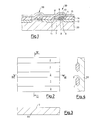
- each cell 30 comprises a semiconductor substrate 20 in which there are obtained diffusions of source 11 and drain 12 essentially of the type n+, between which there is a channel formed by adjacent portions 7, 8, preferably doped in a different way. Over the portions 8 and 7 there are superimposed a layer of cell gate oxide 3 and a transistor oxide layer 9', respectively. Over oxide 3 there is in turn superimposed a first polysilicon strip (perpendicular to the plane of the drawing) constituting a floating gate 4, over which there is an interpoly oxide 9 similar to the transistor oxide 9'. Over oxides 9 and 9' there is arranged a second polysilicon strip constituting a control gate 10. As shown, the floating gate 4 is aligned with the drain diffusion 12 and the control gate 10 is aligned with one edge of the floating gate 4 and with the source and drain diffusions 11 and 12.
- a dielectric 14 is used for sealing the spaces present between one cell and the other and lastly a further polysilicon or silicide strip 15, constituting a connection word-line between cells, extends perpendicularly to the gate strips 4 and 10.
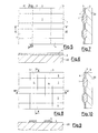
- the process according to the invention for the accomplishment of the pair of cells 30 of Fig. 1 comprises a first step in which on the silicon substrate 20 there are defined parallel insulations strips of field 1 and of active area 2 (Fig.s 2-4). During such step there is also executed the channel implant of the cell (portions 8 and 7 of Fig. 1), necessary for defining the threshold voltage.
- the layer of polysilicon 4 is made conductive (doped) using conventional techniques.
- the double layer of cell gate oxide 3 and polysilicon 4 is defined in strips perpendicular to the field oxide strips 1.
- an implant of transistor channel portion 7 of Fig. 1
- the control gate 10 is differentiated with respect to that in the portion of channel 8 under the floating gate 4.
- transistor gate oxide 9' and of interpoly oxide 9 overwhich there is deposited and made conductive a second layer of polysilicon 10 which shall constitute the control gate.
- a second layer of polysilicon 10 in strips that are parallel and partially superimposed over those of the first layer 4 and then the self-aligned etching of the multilayer constituted by the first and second layer of polysilicon 4, 10, by the interpoly oxide 9 and by the gate oxides 9' and 3 according to strips parallel to one another and perpendicular to the strips related to the field oxide 1 and to the active regions 2.
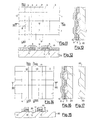
- the field oxide 1 there are uncovered side-by-side regions of source 11 and drain 12, constituting the bitlines, aligned with the control gate 10 and with the floating gate 14, respectively.
- the cell's asymmetry determines the creation of small excavations 30 in the silicon substrate 20 in the source areas 11.
- n+ implant in the regions of source 11 and of drain 12, after which a lateral sealing takes place with oxide 13 of the multistrate 3, 4, 9, 10.
- planarisation is executed, that is, the filling with dielectric 14 of the spaces between the cells 30.
- planarisation is executed by depositing a layer of deposed oxide and subsequently a layer of « spin-on-glass » (or resit) whose object is to make the surface planar.
- Planarisation is completed by partially removing the dielectric 14 and the covering oxide 13 over the second layer of polysilicon 10, so that the polysilicon surfaces 10 are not covered with oxide and may thus be contacted.
- a conductive layer 15 typically polysilicon or silicide, which shall constitute the word-lines.
- the self-aligned etching is executed of the multistrate 3, 4, 9, 10, 15 up to the field oxide 1, according to strips which are parallel to, but wider than, the active area strips 2, so as to obtain cells with lateral fins superimposed over the field oxide 1 (Fig. 32). In this way the fins of one cell are separated from those of the contiguous cell.
Landscapes
- Non-Volatile Memory (AREA)
- Semiconductor Memories (AREA)
Claims (5)
Applications Claiming Priority (2)
| Application Number | Priority Date | Filing Date | Title |
|---|---|---|---|
| IT2284489 | 1989-12-22 | ||
| IT02284489A IT1236980B (it) | 1989-12-22 | 1989-12-22 | Cella di memoria eprom non volatile a gate divisa e processo ad isolamento di campo autoallineato per l'ottenimento della cella suddetta |
Publications (2)
| Publication Number | Publication Date |
|---|---|
| EP0434121A1 EP0434121A1 (fr) | 1991-06-26 |
| EP0434121B1 true EP0434121B1 (fr) | 1995-03-15 |
Family
ID=11201080
Family Applications (1)
| Application Number | Title | Priority Date | Filing Date |
|---|---|---|---|
| EP90203252A Expired - Lifetime EP0434121B1 (fr) | 1989-12-22 | 1990-12-11 | Cellule de mémoire rémanente EPROM à grille divisée et procédé d'isolation de champ auto-aligné pour obtenir cette cellule |
Country Status (5)
| Country | Link |
|---|---|
| US (2) | US5241499A (fr) |
| EP (1) | EP0434121B1 (fr) |
| JP (1) | JP2824702B2 (fr) |
| DE (1) | DE69017863T2 (fr) |
| IT (1) | IT1236980B (fr) |
Families Citing this family (24)
| Publication number | Priority date | Publication date | Assignee | Title |
|---|---|---|---|---|
| US5477068A (en) * | 1992-03-18 | 1995-12-19 | Rohm Co., Ltd. | Nonvolatile semiconductor memory device |
| US5231299A (en) * | 1992-03-24 | 1993-07-27 | International Business Machines Corporation | Structure and fabrication method for EEPROM memory cell with selective channel implants |
| US5508955A (en) * | 1993-05-20 | 1996-04-16 | Nexcom Technology, Inc. | Electronically erasable-programmable memory cell having buried bit line |
| DE69427532T2 (de) * | 1994-02-17 | 2002-04-18 | National Semiconductor Corp., Sunnyvale | Verfahren zur reduzierung den abstandes zwischen den horizontalen benachbarten schwebenden gates einer flash eprom anordnung |
| US5604141A (en) * | 1994-03-15 | 1997-02-18 | National Semiconductor Corporation | Method for forming virtual-ground flash EPROM array with reduced cell pitch in the X direction |
| US5409854A (en) * | 1994-03-15 | 1995-04-25 | National Semiconductor Corporation | Method for forming a virtual-ground flash EPROM array with floating gates that are self aligned to the field oxide regions of the array |
| US5429969A (en) * | 1994-05-31 | 1995-07-04 | Motorola, Inc. | Process for forming electrically programmable read-only memory cell with a merged select/control gate |
| US5712177A (en) * | 1994-08-01 | 1998-01-27 | Motorola, Inc. | Method for forming a reverse dielectric stack |
| US5466624A (en) * | 1994-09-30 | 1995-11-14 | Intel Corporation | Isolation between diffusion lines in a memory array |
| US5445984A (en) * | 1994-11-28 | 1995-08-29 | United Microelectronics Corporation | Method of making a split gate flash memory cell |
| US5597751A (en) * | 1995-12-20 | 1997-01-28 | Winbond Electronics Corp. | Single-side oxide sealed salicide process for EPROMs |
| US5714412A (en) * | 1996-12-02 | 1998-02-03 | Taiwan Semiconductor Manufacturing Company, Ltd | Multi-level, split-gate, flash memory cell and method of manufacture thereof |
| DE69637095D1 (de) * | 1996-12-24 | 2007-07-05 | St Microelectronics Srl | Selbstjustiertes Ätzverfahren zur verwirklichung der Wortleitungen integrierter Halbleiterspeicherbauelemente |
| US5783473A (en) * | 1997-01-06 | 1998-07-21 | Mosel Vitelic, Inc. | Structure and manufacturing process of a split gate flash memory unit |
| DE69731625D1 (de) * | 1997-08-08 | 2004-12-23 | St Microelectronics Srl | Herstellungsprozess von Kreuzpunktspeicherbauelementen mit Zellen, die einen zur Bitleitung und zum Feldoxyd selbstjustierten Source-Kanal aufweisen |
| US6093607A (en) * | 1998-01-09 | 2000-07-25 | Taiwan Semiconductor Manufacturing Company | Method of forming sharp beak of poly by oxygen/fluorine implant to improve erase speed for split-gate flash |
| US6087695A (en) * | 1999-08-20 | 2000-07-11 | Worldwide Semiconductor Mfg | Source side injection flash EEPROM memory cell with dielectric pillar and operation |
| DE10008002C2 (de) * | 2000-02-22 | 2003-04-10 | X Fab Semiconductor Foundries | Split-gate-Flash-Speicherelement, Anordnung von Split-gate-Flash-Speicherelementen und Methode zum Löschen derselben |
| US6403494B1 (en) | 2000-08-14 | 2002-06-11 | Taiwan Semiconductor Manufacturing Company | Method of forming a floating gate self-aligned to STI on EEPROM |
| US6297099B1 (en) | 2001-01-19 | 2001-10-02 | Taiwan Semiconductor Manufacturing Company | Method to free control tunneling oxide thickness on poly tip of flash |
| US7078349B2 (en) * | 2003-07-31 | 2006-07-18 | Taiwan Semiconductor Manufacturing Co., Ltd. | Method to form self-aligned floating gate to diffusion structures in flash |
| KR100525005B1 (ko) * | 2004-05-06 | 2005-10-31 | 삼성전자주식회사 | 스플릿 게이트형 플래쉬 메모리 소자 및 그 제조방법 |
| KR100663344B1 (ko) * | 2004-06-17 | 2007-01-02 | 삼성전자주식회사 | 적어도 두 개의 다른 채널농도를 갖는 비휘발성 플래시메모리 소자 및 그 제조방법 |
| CN108109966B (zh) * | 2018-01-30 | 2021-09-17 | 德淮半导体有限公司 | 静态随机存取存储器及其制造方法 |
Family Cites Families (14)
| Publication number | Priority date | Publication date | Assignee | Title |
|---|---|---|---|---|
| JPS59702B2 (ja) * | 1978-10-18 | 1984-01-07 | トヨタ自動車株式会社 | 燃料噴射式内燃機関の吸気装置 |
| US4274012A (en) * | 1979-01-24 | 1981-06-16 | Xicor, Inc. | Substrate coupled floating gate memory cell |
| JPS5713772A (en) * | 1980-06-30 | 1982-01-23 | Hitachi Ltd | Semiconductor device and manufacture thereof |
| EP0052982B1 (fr) * | 1980-11-20 | 1986-08-13 | Kabushiki Kaisha Toshiba | Dispositif semiconducteur à mémoire et procédé de fabrication |
| JPS5892869A (ja) * | 1981-11-27 | 1983-06-02 | Hitachi Ltd | 配線パターンの欠陥判定方法およびその装置 |
| JPS58206165A (ja) * | 1982-05-26 | 1983-12-01 | Toshiba Corp | 不揮発性半導体メモリ装置 |
| JPS62229982A (ja) * | 1986-03-31 | 1987-10-08 | Toshiba Corp | 半導体記憶装置 |
| GB2200795B (en) * | 1987-02-02 | 1990-10-03 | Intel Corp | Eprom cell with integral select transistor |
| US4785375A (en) * | 1987-06-11 | 1988-11-15 | Tam Ceramics, Inc. | Temperature stable dielectric composition at high and low frequencies |
| FR2626401B1 (fr) * | 1988-01-26 | 1990-05-18 | Sgs Thomson Microelectronics | Memoire eeprom a grille flottante avec transistor de selection de ligne de source |
| JP2844475B2 (ja) * | 1989-07-21 | 1999-01-06 | セイコーインスツルメンツ株式会社 | 半導体不揮発性メモリ |
| IT1235690B (it) * | 1989-04-07 | 1992-09-21 | Sgs Thomson Microelectronics | Procedimento di fabbricazione per una matrice di celle eprom organizzate a tovaglia. |
| JPH02295169A (ja) * | 1989-05-09 | 1990-12-06 | Nec Corp | 不揮発性半導体記憶装置 |
| JPH088313B2 (ja) * | 1989-07-25 | 1996-01-29 | 株式会社東芝 | 不揮発性半導体記憶装置及びその製造方法 |
-
1989
- 1989-12-22 IT IT02284489A patent/IT1236980B/it active IP Right Grant
-
1990
- 1990-12-11 DE DE69017863T patent/DE69017863T2/de not_active Expired - Fee Related
- 1990-12-11 EP EP90203252A patent/EP0434121B1/fr not_active Expired - Lifetime
- 1990-12-19 US US07/631,008 patent/US5241499A/en not_active Expired - Lifetime
- 1990-12-21 JP JP2405095A patent/JP2824702B2/ja not_active Expired - Lifetime
-
1993
- 1993-06-18 US US08/077,934 patent/US5330938A/en not_active Expired - Lifetime
Also Published As
| Publication number | Publication date |
|---|---|
| US5241499A (en) | 1993-08-31 |
| IT8922844A0 (it) | 1989-12-22 |
| IT1236980B (it) | 1993-05-12 |
| EP0434121A1 (fr) | 1991-06-26 |
| JPH0536986A (ja) | 1993-02-12 |
| DE69017863D1 (de) | 1995-04-20 |
| IT8922844A1 (it) | 1991-06-22 |
| US5330938A (en) | 1994-07-19 |
| JP2824702B2 (ja) | 1998-11-18 |
| DE69017863T2 (de) | 1995-08-03 |
Similar Documents
| Publication | Publication Date | Title |
|---|---|---|
| EP0434121B1 (fr) | Cellule de mémoire rémanente EPROM à grille divisée et procédé d'isolation de champ auto-aligné pour obtenir cette cellule | |
| JP2694618B2 (ja) | フラッシュeepromセルアレイとそのアレイの形成方法 | |
| US5923976A (en) | Nonvolatile memory cell and method of fabricating the same | |
| US5411905A (en) | Method of making trench EEPROM structure on SOI with dual channels | |
| US5021848A (en) | Electrically-erasable and electrically-programmable memory storage devices with self aligned tunnel dielectric area and the method of fabricating thereof | |
| US5120672A (en) | Fabricating a single level merged EEPROM cell having an ONO memory stack substantially spaced from the source region | |
| US5420060A (en) | Method of making contract-free floating-gate memory array with silicided buried bitlines and with single-step defined floating gates | |
| US5270240A (en) | Four poly EPROM process and structure comprising a conductive source line structure and self-aligned polycrystalline silicon digit lines | |
| US5019879A (en) | Electrically-flash-erasable and electrically-programmable memory storage devices with self aligned tunnel dielectric area | |
| US4975384A (en) | Erasable electrically programmable read only memory cell using trench edge tunnelling | |
| US4975383A (en) | Method for making an electrically erasable programmable read only memory cell having a three dimensional floating gate | |
| EP0430426A2 (fr) | Dispositif de mémoire semi-conducteur | |
| US5023680A (en) | Floating-gate memory array with silicided buried bitlines and with single-step-defined floating gates | |
| US5469383A (en) | Memory cell array having continuous-strip field-oxide regions | |
| EP0566187A2 (fr) | Dispositif de mémoire rémanente en forme de tranchée et méthode d'auto-alignement pour le fabriquer | |
| US5479036A (en) | Fieldless split-gate EPROM/Flash EPROM | |
| USRE35356E (en) | EEPROM cell array with tight erase distribution | |
| US5120571A (en) | Floating-gate memory array with silicided buried bitlines and with single-step-defined floating gates | |
| US6410957B1 (en) | Method of forming poly tip to improve erasing and programming speed in split gate flash | |
| US6124157A (en) | Integrated non-volatile and random access memory and method of forming the same | |
| US6429076B2 (en) | Flash EPROM memory cell having increased capacitive coupling and method of manufacture thereof | |
| US5365082A (en) | MOSFET cell array | |
| US5200350A (en) | Floating-gate memory array with silicided buried bitlines | |
| EP0731983B1 (fr) | Isolation amelioree entre les lignes de diffusion d'une memoire | |
| EP0368097A2 (fr) | Matrice de mémoires à porte flottante croisée sans contacts ayant des lignes de bit enterrées en siliciure |
Legal Events
| Date | Code | Title | Description |
|---|---|---|---|
| PUAI | Public reference made under article 153(3) epc to a published international application that has entered the european phase |
Free format text: ORIGINAL CODE: 0009012 |
|
| AK | Designated contracting states |
Kind code of ref document: A1 Designated state(s): DE FR GB SE |
|
| 17P | Request for examination filed |
Effective date: 19911210 |
|
| 17Q | First examination report despatched |
Effective date: 19931103 |
|
| GRAA | (expected) grant |
Free format text: ORIGINAL CODE: 0009210 |
|
| AK | Designated contracting states |
Kind code of ref document: B1 Designated state(s): DE FR GB SE |
|
| REF | Corresponds to: |
Ref document number: 69017863 Country of ref document: DE Date of ref document: 19950420 |
|
| ET | Fr: translation filed | ||
| PG25 | Lapsed in a contracting state [announced via postgrant information from national office to epo] |
Ref country code: SE Effective date: 19950615 |
|
| PLBE | No opposition filed within time limit |
Free format text: ORIGINAL CODE: 0009261 |
|
| STAA | Information on the status of an ep patent application or granted ep patent |
Free format text: STATUS: NO OPPOSITION FILED WITHIN TIME LIMIT |
|
| 26N | No opposition filed | ||
| REG | Reference to a national code |
Ref country code: FR Ref legal event code: D6 |
|
| PGFP | Annual fee paid to national office [announced via postgrant information from national office to epo] |
Ref country code: GB Payment date: 20011212 Year of fee payment: 12 Ref country code: FR Payment date: 20011212 Year of fee payment: 12 |
|
| REG | Reference to a national code |
Ref country code: GB Ref legal event code: IF02 |
|
| PGFP | Annual fee paid to national office [announced via postgrant information from national office to epo] |
Ref country code: DE Payment date: 20020109 Year of fee payment: 12 |
|
| PG25 | Lapsed in a contracting state [announced via postgrant information from national office to epo] |
Ref country code: GB Free format text: LAPSE BECAUSE OF NON-PAYMENT OF DUE FEES Effective date: 20021211 |
|
| PG25 | Lapsed in a contracting state [announced via postgrant information from national office to epo] |
Ref country code: DE Free format text: LAPSE BECAUSE OF NON-PAYMENT OF DUE FEES Effective date: 20030701 |
|
| GBPC | Gb: european patent ceased through non-payment of renewal fee | ||
| PG25 | Lapsed in a contracting state [announced via postgrant information from national office to epo] |
Ref country code: FR Free format text: LAPSE BECAUSE OF NON-PAYMENT OF DUE FEES Effective date: 20030901 |
|
| REG | Reference to a national code |
Ref country code: FR Ref legal event code: ST |