EP0430426A2 - Dispositif de mémoire semi-conducteur - Google Patents
Dispositif de mémoire semi-conducteur Download PDFInfo
- Publication number
- EP0430426A2 EP0430426A2 EP90311578A EP90311578A EP0430426A2 EP 0430426 A2 EP0430426 A2 EP 0430426A2 EP 90311578 A EP90311578 A EP 90311578A EP 90311578 A EP90311578 A EP 90311578A EP 0430426 A2 EP0430426 A2 EP 0430426A2
- Authority
- EP
- European Patent Office
- Prior art keywords
- oxide
- region
- gate
- junction
- floating gate
- Prior art date
- Legal status (The legal status is an assumption and is not a legal conclusion. Google has not performed a legal analysis and makes no representation as to the accuracy of the status listed.)
- Withdrawn
Links
Images
Classifications
-
- H—ELECTRICITY
- H10—SEMICONDUCTOR DEVICES; ELECTRIC SOLID-STATE DEVICES NOT OTHERWISE PROVIDED FOR
- H10B—ELECTRONIC MEMORY DEVICES
- H10B69/00—Erasable-and-programmable ROM [EPROM] devices not provided for in groups H10B41/00 - H10B63/00, e.g. ultraviolet erasable-and-programmable ROM [UVEPROM] devices
-
- H—ELECTRICITY
- H10—SEMICONDUCTOR DEVICES; ELECTRIC SOLID-STATE DEVICES NOT OTHERWISE PROVIDED FOR
- H10D—INORGANIC ELECTRIC SEMICONDUCTOR DEVICES
- H10D30/00—Field-effect transistors [FET]
- H10D30/60—Insulated-gate field-effect transistors [IGFET]
- H10D30/68—Floating-gate IGFETs
- H10D30/681—Floating-gate IGFETs having only two programming levels
- H10D30/684—Floating-gate IGFETs having only two programming levels programmed by hot carrier injection
- H10D30/685—Floating-gate IGFETs having only two programming levels programmed by hot carrier injection from the channel
Definitions
- the present invention relates to semiconductor memory cells in general and more particularly to a non-volatile memory cell including a programmable and erasable floating gate structure.
- MOS metal-oxide-semiconductor
- Non-volatile MOS memory utilized an application of radiation, typically ultraviolet light, to accomplish erasure of the memory cells.
- radiation typically ultraviolet light
- Flash EEPROM is an electrically-erasable, programmable ROM in which all or almost all of the cells may be erased simultaneously.
- non-volatile memory devices There remain, however, a variety of problems confronting designers of non-volatile memory devices.
- One almost universally desired goal is the achievement of small cell size. Compared to typical standard MOS transistors and even to various dynamic random access memory cells, non-volatile cells are rather large. For various reasons, non-volatile cells cannot always be easily scaled downward as semiconductor process linewidths and feature sizes decrease.
- the current trend in array design is toward the use of "virtual ground” arrays.
- the virtual ground array may be made locally “contactless.” There is no need to create space-consuming windows above the source/drain junctions because the junctions themselves may serve as buried bit lines.
- the present invention features a memory device with means for controlling current flow, for example, control, floating, and erase gates.
- One junction region of the device is "buried" in the substrate under a comparatively thick oxide, while the other junction reaches the substrate surface.
- the junction which reaches the surface may, if desired, be contacted via an opening in an overlying dielectric.
- the basic memory cell is small, and may be arranged into a compact non-virtual-ground-type array.
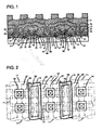
- FIG. 1 is a cross-sectional view of a typical pair of devices according to the presentinvention.
- Reference numeral 9 denotes a substrate which for purposes of the present discussion is assumed to be p-type. An n-type substrate may also be used, in which case, of course, the dopings of the various buried regions and all junction areas to be discussed in the following paragraphs must be changed from n to p and vice versa.
- Reference numeral 15 denotes a buried n+ region, while reference numerals 17 and 17′ denote p+ regions.
- Thick oxide region 13 (termed "buried n+ oxide”) overlies region 15.
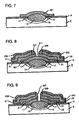
- FIGs. 4-6 indicate the manner in which buried n+ oxide region 13 together with buried n+ region 15 and p+ regions 17 and 17′ are fabricated.
- FIG. 4 there is shown a typical cross-section of a semiconductor wafer during the initial steps of fabrication.
- Reference numeral 101 denotes a pad oxide and reference numeral 103 denotes a patterned nitride layer formed by techniques well known to those skilled in the art.
- Patterned layer 103 has opening 105.
- a p-type ion implantation for example, with boron ions, is performed through opening 105, producing a buried p+ region 107.
- a thermal drive-in step is performed to further diffuse the p+ species.
- a second ion implantation with n-type ions, for example arsenic, is performed to produce a buried n+ region 109 as shown in FIG. 5.
- n+ and p+ regions are illustrated in FIG. 5 with the buried p+ region denoted by reference numeral 107 extending somewhat further laterally than the buried n+ region 109 because of the previously-mentioned thermal drive-in step.
- a thermal oxide 13 is grown in opening 105, as shown in FIG. 6, by conventional processes.
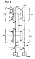
- Field oxide 11 shown in the top view of FIG. 2 may be grown at the same time. (Thus, when layers 103 and 101 are patterned, they may be patterned for both field oxide 11 and buried n+ oxide 13. Of course, the exposed silicon in the regions designated for subsequent field oxide growth must be shielded with a resist from the ion implantation steps described above.)
- the reference numerals of the buried ergions in FIG. 6 have been re-adjusted to conform to the reference numerals of the completely formed regions in FIG. 1.
- the reference numeral 107 has been changed to 17 and 17′ and reference numeral 109 has been changed to 15.
- FIGs. 4-6 have illusrated the manner in which buried n+ oxide 13 together with buried n+ region 15 and buried p+ regions 17 and 17′, all illustrated in FIG. 1, are formed.
- a highly desirable feature of the disclosed process is that no separate masking step is required to form buried p+ regions 17 and 17′.
- the buried p+ regions may extend laterally outward as far as the edge of floating gates 21 and 23.
- Oxide region 13 (“buried n+ oxide”) is not a field oxide (although it is grown by similar processes). Oxide region 13, as will be subsequently explained, does not serve to isolate two transistors in the way that a conventional field oxide isolates two transistors. As will be subsequently detailed, buried n+ region 15 is shared by two transistor-like cells. Furthermore, oxide region 13 provides a platform for the processing steps to be described below which create structures 23, 25, and 59 (FIG. 1). Such processing (which involves general etching and depositions) cannot reliably be carried out over a thin oxide region. Other features and advantages of oxide region 13 will be mentioned in later paragraphs. Typically, the total thickness of oxide region 13 is 3000 ⁇ although thickness between 1000 ⁇ and 6000 ⁇ are acceptable.
- dielectric preferably silicon oxide
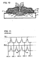
- FIGs. 7-10 illustrate some of the principal fabrication steps involved in forming floating gates 21 and 23.
- patterned polysilicon layer 201 (which will eventually become floating gates 21 and 23) has been deposited over buried n+ oxide 13 and oxide layer 19.
- Layer 201 has a stepped profile because it extends over buried n+ oxide 13.
- oxide layer 31 is grown over polysilicon layer 201. Then a second polysilicon layer is deposited, covered by an oxide layer, and subsequently patterned to form control gates 25 and 27 with overlying 203 and 205 respectively. After polysilicon layers 25 and 27 have been formed, an additional oxide layer is deposited on top (of layers 203 and 205) and anisotropically etched to produce spacers 207 and 209 and opening 211. If desired, a double spacer may be formed by deposition and subsequent etching of two different types of glass.
- polysilicon layer 201 has been cut or severed, forming floating gates 21 and 23 by anisotropic etching through opening 211 defined by spacers 207 and 209.
- the spacer technique illustrated in FIGs. 7-9 permits the self-alignment of, for example, floating gate 23 with control gate 25 and floating gate 21 with control gate 27.
- spacers 207 and 209 have been etched back somewhat to expose top surfaces 41 and 43 of floating gates 21 and 23 respectively.
- the outer spacer may be etched away to expose surfaces 41 and 43.
- An etch process which preferentially attacks the outer spacer without damaging the inner spacer may be used.
- an additional oxide layer (50 in FIG. 1) is formed over control gates 25 and 27.
- the additional oxide layer also covers surfaces 41 and 43, together with surfaces 45 and 47 (i.e., the sides of floating gates 21 and 23 respectively).
- the oxide is preferably grown in a manner which produces asperities in surfaces 41 and 43.
- windows 51 and 53 are lithographically defined and opened.
- the window opening exposes the bare upper surface of silicon substrate 9.
- a third layer of polysilicon is blanket-deposited and patterned.
- the patterned polysilicon produces structures 55, 57, and 59.
- Structure 59 is the erase gate whose operation will be described in greater detail later.
- Structures 55 and 57 are termed "landing pads.” It will be noted that the deposition of the third polysilicon layer conveniently forms erase gate 59 while simultaneously forming polysilicon landing pads 55 and 57.
- landing pads 55 and 57 have a flower-vase-like shape
- erase gate 59 has a shape somewhat reminiscent of an elongated trough.
- the landing pads have protrusions 81 and 83 which extend laterally beyond the original window dimensions.
- Junction regions 61 and 63 may be formed either by ion implantaton after windows 51 and 53 have been opened or by diffusion of dopant species from polysilicon landing pads 55 and 57 by techniques well known to those skilled in the art.
- passivation dielectric layer 71 is deposited.
- next steps in fabrication of the inventive device involve opening windows 73 and 75 in dielectric 71 and blanket deposition and patterning of metal layer 76 (which will form the column line in the about-to-be-discussed array).
- Dielectric layer 77 is then deposited over metal line 76.
- a subsequently deposited metal layer may be patterned and contacted through vias to control gates 25 and 27.
- the metal layer terms a "strap" may enhance the speed of the device.
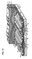
- FIGs. 1 and 12 will reveal a few salient features of the inventive device. It will be noted (and made clearer below) that the cross-section of FIG. 1 shows two back-to-back (or mirror image) devices. One device has junctions 15 and 61 with floating gate 23 and control gate 25. The other device has junctions 15 and 63 with floating gate 21 and control gate 27. Thus, junction 15 beneath buried n+ oxide 13 is shared by both devices. Furthermore, erase gate 59 is also shared by both devices.
- FIG. 12 illustrates that erase gate 59 extends to cover a multiplicity of pairs of devices (i.e., a pair of rows in the soon-to-be-described array). Similarly, control gates 25 and 27 extend to cover entire rows of devices. However, floating gates 23 and 21 do not extend continuously, as can be seen from the diagram in FIG. 2. There is one discrete floating gate per cell.
- each cell pair has one polysilicon landing pad, for example reference numeral 73 or 75.
- Each landing pad has an upper protrusion 81 or 83 which permits some misalignment of the window through which metal layer 76 is later deposited.
- FIG. 1 the reading, writing and erasing operations of an individual cell will be described.
- FIG. 1 essentially depicts two back-to-back or mirror-image transistors.
- the present discussion will focus on the right-hand transistor cell for convenience. Operation of the left-hand transistor is similar. It may be convenient to consider buried n+ region 15 and junction 61 as akin to drain/source regions. Approximately 12-15 volts is applied to the word-line of the array in which the inventive device is located (to be described later) which is connected to control gate 25. Buried n+ region 15 is at approximately 8-10 volts, while junction 61 is grounded. Under these conditions, electrons are injected into floating gate 23 by hot carrier injection. Buried p+ region 17 serves to enhance the efficiency of the hot carrier injection mechanism.
- Buried p+ region 17 essentially decreases the size of the depletion region created in the channel between junction 61 and buried n+ region 15, thus increasing the lateral electric field.
- the higher lateral electric field enhances hot carrier injection into floating gate 23.
- the threshold voltage of the cell transistor between regions 15 and 61 has been increased. This increase in threshold voltage may be subsequently detected and interpreted as a "1" or "0".
- Erasing essentially consists of removing the electronic charge from floating gate 23.
- a high voltage is applied to erase gate 59. Typically, the applied high voltage is between 12 and 24 volts.
- Control gate 25 is grounded, while regions 15 and 61 are also grounded. Charge tunnels from floating gate 23 through the oxide 50 between floating gate 23 and erase gate 59. Thus, the charge stored on control gate 23 has been removed and the threshold voltage of the transistor between regions 15 and 61 returns to its previous value.
- Reading is the operation by which the presence or absence of charge on the floating gate 23 is detected. Five volts is applied to control gate 25; buried n+ region 15 is grounded. If charge is stored on floating gate 23, the threshold voltage of the transistor device between regions 15 and 61 will be higher than five volts and no current will flow in the cell. If there is no charge stored on floating gate 23, then the cell will turn on and the current can be sensed by a sense amplifier to be described later.
- erase gate 59 not only has the ability to erase the right-hand transistor, but also the left-hand transistor at the same time.
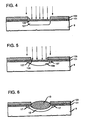
- FIG. 3 illustrates how the pair of mirror-image cells depicted in FIG. 1 may be combined into a memory array 400. Reading, writing, and erasing of an individual cell within array 400 will now be described.
- FIG. 3 illustrates transistor cell pairs 401, 403, 405, and 407. Each of the cell pairs has a cross-section similar to that shown in FIG. 1.
- the reference numerals employed in FIG. 3 suggest correspondence between various circuit schematic elements and the appropriate device physical regions illustrated in FIG. 1.
- erase gate 59 illustrated in FIG. 1 is shown schematically in FIG. 3; buried n+ region illustrated in FIG. 1 is shown schematically as node 15 in FIG. 3, etc.
- Control gate 25 is raised to 12-15 volts via "line" 525 (which is actually the continuous polysilicon sheet control gate 25 shown in cross-section in FIG.
- Erasing will next be descirbed. Erasing may be accomplished by erasing cell pairs, such as 401, 403, 405, or 407 by simply energizing the erase gate 59 in the manner previously described. Thus, entire row pairs may be erased in a "flash.” Of course, if desired, the entire array may be erased simultaneously or pair by pair.
- Control gate 25 of the selected row for example the row containing the transistor between junctions 15 and 61 is raised to 5 volts, while the control gate of non-selected rows is maintained at ground. Node 15 is grounded.
- sense amplifier 301 will sense current flow in the transistor between junctions 15 and 61, if there is no charge stored on floating gate 23 otherwise, no current will be sensed.
- Select transistor 601 and 603 select the column to be read by sense amplifiers 301 and 303 so that an entire word may be read at once. Of, if desired, separate select transistors may be used to read groups of bit lines at a time.
- Polysilicon landing pads 73 and 75 (which were formed in the same step as erase gate 59) have protrusions 81 and 83. Protrusions 81 and 83 extend outward beyond the extent of junction region 61 and permit some misalignment of the window 51, 53 opening. Thus, if the mask used to create windows 51 and 53 is slightly misaligned with respect to junctions 61 and 63 protrusions 81 and 83 will nevertheless permit effective contact to be made between metal layer 76 and junctions 61 and 63. The use of landing pads such as 55 and 57 is believed heretofore unknown in non-volatile memory cells.
- two transistor cells share a common erase gate, for example reference numeral 59 in FIG. 1, thus permitting a higher cell packing density.
- FIGs. 7-10 produces self-aligned floating gate 23 and control gate 25. Consequently, there is no chance of misalignment between the floating gate and control gate.
- Buried n+ oxide 13 serves to enhance the coupling ratio which is the ratio of the capacitance between floating gate 23 and control gate 25 divided by the total capacitance associated with floating gate 23. An improved coupling ratio increases the programming efficiency of the cell.
- FIG. 11 indicates a typical prior art virtual ground array.
- the figure illustrates five columns and two word lines.
- pattern sensitivity One problem exhibited by the virtual ground array is termeds "pattern sensitivity."
- the loading of a particular column depends upon the states of the neighboring transistors.
- the loading at node designated 700 in FIG. 11 depends upon the states of the transistors to the left of node 700, while the loading seen at node 701 depends upon the status of those cells to the right of 701. Consequently, the reading speed of a particular cell varies according to the pattern stored in the entire array.
- fault propagation Another difficulty with a typical virtual ground array is termed "fault propagation." Should any column, for example, column 2 be shorted to ground, then other columns will "see” the ground if a transistor (or series of transistors) between the two columns is turned on. Consequently, depending upon the pattern stored in the array, if one column line fails (i.e., becomes grounded), a variety of other column lines may also be similarly affected via a network of "turned on” transistors. This difficulty cannot be repaired by redundancy.
- each column is independent as can be seen from FIG. 3, and it may be replaced by a redundant column.
- the fault propagation problem can, of course, affect the manufacturing yield of wafers with virtual ground devices since a device with a defective column cannot be repaired and must be discarded.
- the array depicted in FIG. 3 is a NOR-type array which has fallen somewhat out of favor with non-volatile designers since it requires windowed contacts to individual cells although it does not exhibit the aforementioned problems of pattern sensitivity and fault propagation.
- field oxide 11 extends lengthwise between two cells. Consequently, if the cell size is shrunk lengthwise, the field oxide's critical dimension (i.e., width) is not affected. Designs with comparatively smaller field oxides (relative to total cell size) do not scale downward as easily because the field oxide structure, when shrunk tends to exhibit rounded corners and, because of the formation of long birds' beaks the field oxide maximum thickness is suppressed.
- the unique inventive cell design depicted in FIG. 1 permits incorporation into an array which avoids the disadvantages of the commonly used virtual ground array, thus permitting small cell size together with the attendant advantages of high yield, high speed, and high reliability.
Landscapes
- Non-Volatile Memory (AREA)
- Semiconductor Memories (AREA)
Applications Claiming Priority (2)
| Application Number | Priority Date | Filing Date | Title |
|---|---|---|---|
| US07/430,390 US5036378A (en) | 1989-11-01 | 1989-11-01 | Memory device |
| US430390 | 1989-11-01 |
Publications (2)
| Publication Number | Publication Date |
|---|---|
| EP0430426A2 true EP0430426A2 (fr) | 1991-06-05 |
| EP0430426A3 EP0430426A3 (en) | 1991-06-12 |
Family
ID=23707360
Family Applications (1)
| Application Number | Title | Priority Date | Filing Date |
|---|---|---|---|
| EP19900311578 Withdrawn EP0430426A3 (en) | 1989-11-01 | 1990-10-23 | Semiconductor memory device |
Country Status (3)
| Country | Link |
|---|---|
| US (1) | US5036378A (fr) |
| EP (1) | EP0430426A3 (fr) |
| JP (1) | JPH03155168A (fr) |
Cited By (2)
| Publication number | Priority date | Publication date | Assignee | Title |
|---|---|---|---|---|
| WO1994001892A1 (fr) * | 1992-07-03 | 1994-01-20 | Commissariat A L'energie Atomique | Memoire eeprom de type flash a triples grilles et son procede de fabrication |
| GB2299449A (en) * | 1995-03-22 | 1996-10-02 | Hyundai Electronics Ind | Flash EEPROM cell |
Families Citing this family (23)
| Publication number | Priority date | Publication date | Assignee | Title |
|---|---|---|---|---|
| US5196914A (en) * | 1989-03-15 | 1993-03-23 | Sgs-Thomson Microelectronics S.R.L. | Table cloth matrix of EPROM memory cells with an asymmetrical fin |
| JP2807304B2 (ja) * | 1990-02-19 | 1998-10-08 | 株式会社東芝 | 不揮発性半導体装置 |
| US5212541A (en) * | 1991-04-18 | 1993-05-18 | National Semiconductor Corporation | Contactless, 5v, high speed eprom/flash eprom array utilizing cells programmed using source side injection |
| US5138576A (en) * | 1991-11-06 | 1992-08-11 | Altera Corporation | Method and apparatus for erasing an array of electrically erasable EPROM cells |
| US5723888A (en) * | 1993-05-17 | 1998-03-03 | Yu; Shih-Chiang | Non-volatile semiconductor memory device |
| US5436480A (en) * | 1993-02-22 | 1995-07-25 | Yu; Shih-Chiang | Integrated circuit interconnection programmable and erasable by a plurality of intersecting control traces |
| US5702979A (en) * | 1994-05-31 | 1997-12-30 | Sgs-Thomson Microelectronics, Inc. | Method of forming a landing pad structure in an integrated circuit |
| US5956615A (en) * | 1994-05-31 | 1999-09-21 | Stmicroelectronics, Inc. | Method of forming a metal contact to landing pad structure in an integrated circuit |
| US5945738A (en) * | 1994-05-31 | 1999-08-31 | Stmicroelectronics, Inc. | Dual landing pad structure in an integrated circuit |
| US5455792A (en) * | 1994-09-09 | 1995-10-03 | Yi; Yong-Wan | Flash EEPROM devices employing mid channel injection |
| JP4156044B2 (ja) * | 1994-12-22 | 2008-09-24 | エスティーマイクロエレクトロニクス,インコーポレイテッド | 集積回路におけるランディングパッド構成体の製造方法 |
| US5705427A (en) * | 1994-12-22 | 1998-01-06 | Sgs-Thomson Microelectronics, Inc. | Method of forming a landing pad structure in an integrated circuit |
| US5579259A (en) * | 1995-05-31 | 1996-11-26 | Sandisk Corporation | Low voltage erase of a flash EEPROM system having a common erase electrode for two individually erasable sectors |
| US5597751A (en) * | 1995-12-20 | 1997-01-28 | Winbond Electronics Corp. | Single-side oxide sealed salicide process for EPROMs |
| US5719071A (en) * | 1995-12-22 | 1998-02-17 | Sgs-Thomson Microelectronics, Inc. | Method of forming a landing pad sturcture in an integrated circuit |
| KR100215883B1 (ko) | 1996-09-02 | 1999-08-16 | 구본준 | 플래쉬 메모리 소자 및 그 제조방법 |
| US5768186A (en) * | 1996-10-25 | 1998-06-16 | Ma; Yueh Yale | High density single poly metal-gate non-volatile memory cell |
| JPH1187539A (ja) | 1997-09-04 | 1999-03-30 | Mitsubishi Electric Corp | 不揮発性半導体記憶装置およびその製造方法 |
| TW434907B (en) * | 1998-12-09 | 2001-05-16 | Matsushita Electronics Corp | Semiconductor memory apparatus and its manufacturing method |
| US6153517A (en) * | 1999-03-12 | 2000-11-28 | Taiwan Semiconductor Manufacturing Company | Low resistance poly landing pad |
| US6483144B2 (en) | 1999-11-30 | 2002-11-19 | Agere Systems Guardian Corp. | Semiconductor device having self-aligned contact and landing pad structure and method of forming same |
| US7057928B2 (en) * | 2003-07-08 | 2006-06-06 | Hewlett-Packard Development Company, L.P. | System and method for erasing high-density non-volatile fast memory |
| US8844602B2 (en) * | 2008-11-21 | 2014-09-30 | Sumitomo Electric Industries, Ltd. | Method of processing terminus of optical fiber and terminus processing tool |
Family Cites Families (12)
| Publication number | Priority date | Publication date | Assignee | Title |
|---|---|---|---|---|
| US4409723A (en) * | 1980-04-07 | 1983-10-18 | Eliyahou Harari | Method of forming non-volatile EPROM and EEPROM with increased efficiency |
| US4361847A (en) * | 1980-04-07 | 1982-11-30 | Eliyahou Harari | Non-volatile EPROM with enhanced drain overlap for increased efficiency |
| JPS5743470A (en) * | 1980-08-29 | 1982-03-11 | Fujitsu Ltd | Semiconductor device |
| US4558344A (en) * | 1982-01-29 | 1985-12-10 | Seeq Technology, Inc. | Electrically-programmable and electrically-erasable MOS memory device |
| US4490900A (en) * | 1982-01-29 | 1985-01-01 | Seeq Technology, Inc. | Method of fabricating an MOS memory array having electrically-programmable and electrically-erasable storage devices incorporated therein |
| US4701776A (en) * | 1983-08-29 | 1987-10-20 | Seeq Technology, Inc. | MOS floating gate memory cell and process for fabricating same |
| US4750024A (en) * | 1986-02-18 | 1988-06-07 | Texas Instruments Incorporated | Offset floating gate EPROM memory cell |
| US4855800A (en) * | 1986-03-27 | 1989-08-08 | Texas Instruments Incorporated | EPROM with increased floating gate/control gate coupling |
| JPH0687500B2 (ja) * | 1987-03-26 | 1994-11-02 | 日本電気株式会社 | 半導体記憶装置およびその製造方法 |
| JP2735193B2 (ja) * | 1987-08-25 | 1998-04-02 | 株式会社東芝 | 不揮発性半導体装置及びその製造方法 |
| US4853895A (en) * | 1987-11-30 | 1989-08-01 | Texas Instruments Incorporated | EEPROM including programming electrode extending through the control gate electrode |
| US4844776A (en) * | 1987-12-04 | 1989-07-04 | American Telephone And Telegraph Company, At&T Bell Laboratories | Method for making folded extended window field effect transistor |
-
1989
- 1989-11-01 US US07/430,390 patent/US5036378A/en not_active Expired - Lifetime
-
1990
- 1990-10-23 EP EP19900311578 patent/EP0430426A3/en not_active Withdrawn
- 1990-11-01 JP JP2293783A patent/JPH03155168A/ja active Pending
Cited By (3)
| Publication number | Priority date | Publication date | Assignee | Title |
|---|---|---|---|---|
| WO1994001892A1 (fr) * | 1992-07-03 | 1994-01-20 | Commissariat A L'energie Atomique | Memoire eeprom de type flash a triples grilles et son procede de fabrication |
| GB2299449A (en) * | 1995-03-22 | 1996-10-02 | Hyundai Electronics Ind | Flash EEPROM cell |
| GB2299449B (en) * | 1995-03-22 | 1999-04-14 | Hyundai Electronics Ind | Flash eeprom cell and manufacturing methods thereof |
Also Published As
| Publication number | Publication date |
|---|---|
| EP0430426A3 (en) | 1991-06-12 |
| JPH03155168A (ja) | 1991-07-03 |
| US5036378A (en) | 1991-07-30 |
Similar Documents
| Publication | Publication Date | Title |
|---|---|---|
| US5036378A (en) | Memory device | |
| US5554553A (en) | Highly compact EPROM and flash EEPROM devices | |
| US5268318A (en) | Highly compact EPROM and flash EEPROM devices | |
| US5198380A (en) | Method of highly compact EPROM and flash EEPROM devices | |
| KR100217532B1 (ko) | 플래시 메모리를 위한 향상된 팩킹 밀도 | |
| US5168465A (en) | Highly compact EPROM and flash EEPROM devices | |
| US6849501B2 (en) | Methods for fabricating an improved floating gate memory cell | |
| US5464999A (en) | Method for programming an alternate metal/source virtual ground flash EPROM cell array | |
| US5150179A (en) | Diffusionless source/drain conductor electrically-erasable, electrically-programmable read-only memory and method for making and using the same | |
| EP0349774A2 (fr) | Dispositifs eprom et flash-eeprom hautement compacts | |
| US5962891A (en) | Nonvolatile semiconductor memory device | |
| US20030031068A1 (en) | Non-volatile memory cell array having discontinuous source and drain diffusions contacted by continuous bit line conductors and methods of forming | |
| EP0434121B1 (fr) | Cellule de mémoire rémanente EPROM à grille divisée et procédé d'isolation de champ auto-aligné pour obtenir cette cellule | |
| JPS639981A (ja) | 減少したトンネルエリアを有する電気的に変更できる持久記憶浮動ゲ−ト型メモリデバイスとその製造方法 | |
| US5168335A (en) | Electrically programmable, electrically erasable memory array cell with field plate | |
| EP0573728B1 (fr) | Procédé de fabrication d'EPROM sans contacts à haute densité d'intégration | |
| US6060358A (en) | Damascene NVRAM cell and method of manufacture | |
| US4994403A (en) | Method of making an electrically programmable, electrically erasable memory array cell | |
| US5086410A (en) | Non-erasable eprom cell for redundancy circuit | |
| EP0557754A2 (fr) | Contacts autoalignés pour circuits intégrés à dispositifs à effet de champ complémentaires | |
| US5340768A (en) | Method of fabricating self-aligned field-plate isolation between control electrodes | |
| EP1191597A2 (fr) | Procédé de fabrication de parois pour améliorant les performances d'un mémoire flash | |
| US5151760A (en) | Integrated circuit with improved capacitive coupling | |
| US6778438B2 (en) | Structure, fabrication method and operating method for flash memory | |
| EP0673071B1 (fr) | Mémoire flash EEPROM et matrices EPROM |
Legal Events
| Date | Code | Title | Description |
|---|---|---|---|
| PUAI | Public reference made under article 153(3) epc to a published international application that has entered the european phase |
Free format text: ORIGINAL CODE: 0009012 |
|
| PUAL | Search report despatched |
Free format text: ORIGINAL CODE: 0009013 |
|
| AK | Designated contracting states |
Kind code of ref document: A2 Designated state(s): DE FR GB IT |
|
| AK | Designated contracting states |
Kind code of ref document: A3 Designated state(s): DE FR GB IT |
|
| 17P | Request for examination filed |
Effective date: 19911203 |
|
| 17Q | First examination report despatched |
Effective date: 19930408 |
|
| RAP3 | Party data changed (applicant data changed or rights of an application transferred) |
Owner name: AT&T CORP. |
|
| STAA | Information on the status of an ep patent application or granted ep patent |
Free format text: STATUS: THE APPLICATION IS DEEMED TO BE WITHDRAWN |
|
| 18D | Application deemed to be withdrawn |
Effective date: 19940624 |