EP0434355A2 - Differenzieller Phasendemodulator für phasensprungmodulierte Signale - Google Patents
Differenzieller Phasendemodulator für phasensprungmodulierte Signale Download PDFInfo
- Publication number
- EP0434355A2 EP0434355A2 EP90313815A EP90313815A EP0434355A2 EP 0434355 A2 EP0434355 A2 EP 0434355A2 EP 90313815 A EP90313815 A EP 90313815A EP 90313815 A EP90313815 A EP 90313815A EP 0434355 A2 EP0434355 A2 EP 0434355A2
- Authority
- EP
- European Patent Office
- Prior art keywords
- signal
- producing
- zero
- baud
- timing signal
- Prior art date
- Legal status (The legal status is an assumption and is not a legal conclusion. Google has not performed a legal analysis and makes no representation as to the accuracy of the status listed.)
- Withdrawn
Links
Images


Classifications
-
- H—ELECTRICITY
- H04—ELECTRIC COMMUNICATION TECHNIQUE
- H04L—TRANSMISSION OF DIGITAL INFORMATION, e.g. TELEGRAPHIC COMMUNICATION
- H04L27/00—Modulated-carrier systems
- H04L27/18—Phase-modulated carrier systems, i.e. using phase-shift keying
- H04L27/22—Demodulator circuits; Receiver circuits
- H04L27/233—Demodulator circuits; Receiver circuits using non-coherent demodulation
- H04L27/2335—Demodulator circuits; Receiver circuits using non-coherent demodulation using temporal properties of the received signal
- H04L27/2337—Demodulator circuits; Receiver circuits using non-coherent demodulation using temporal properties of the received signal using digital techniques to measure the time between zero-crossings
Definitions
- the present invention relates to a demodulator for PSK-demodulating intermediate frequency (IF) signals of a PSK-modulated carrier with digital data, and more particularly to a demodulator of this kind using differential detection.
- IF intermediate frequency
- One of the prior art differential phase demodulators or differential detection demodulators of this kind achieves data demodulation by determining the phase variation during a one-baud interval after converting an IF signal into I and Q baseband channels.
- a demodulator involves the drawbacks of having complex configuration, which makes it difficult for the circuit to be arranged in small dimensions, and many aspects needing adjustment, such as the linearity and gain of the frequency discriminator and the balance between the I and Q baseband channels.
- Another prior art demodulator which comprises a frequency discriminator and an integrate and dump (ID) circuit is subject to a greater error rate depending on the phase varying condition of input signals besides the need to adjust the constituent elements of the circuit to achieve overall characteristics of the demodulator.
- ID integrate and dump
- An object of the present invention is to provide a differential phase demodulator which permits arrangement in small dimensions and requires no adjustment.
- Another object of the invention is to provide a timing extraction circuit which is suitable for a differential phase demodulator and capable of readily extracting baud timings from input signals.
- a PSK-modulated signal demodulating circuit comprising a zero-cross detector for receiving an intermediate frequency (IF) signal of a PSK-modulated carrier, detecting the zero-cross point of the IF signals and generating a zero-cross detection signal.
- a synchronizing circuit receives an externally supplied baud timing signal extracted from the IF signal and the zero-cross signal, and supplies a synchronized baud timing signal by synchronizing the baud timing signal with the zero-cross signal.
- An oscillator generates clock pulse signals having a predetermined frequency.
- a counter receives the clock pulse signals, counts the clock pulses and supplies the pulse count.
- a phase difference detector receives the pulse count and the synchronized baud timing signal, calculates the count per period of the synchronized baud timing signal and supplies the result as the phase difference data.
- a decision circuit receives the phase difference data, decide received data based on the phase difference data and supplies the result of decision as the received data.
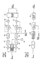
- the differential detection demodulator includes first to fourth multipliers 101, 107, 105 and 112, first and second low-pass filters 102 and 108, first and second analog-to-digital (A/D) converters 103 and 110, first and second latches 104 and 111, a decision circuit 106, a local oscillator 109 and a quadrature signal generator 113.
- An intermediate frequency (IF) signal of a digitally phase-modulated, for instance a QPSK-modulated, input signal are supplied to the first and second multipliers 101 and 107.
- a reference signal, having a frequency almost equal to that of the input IF signal, generated by the local oscillator 109 is fed to the quadrature signal generator 113, which supplies the reference signal, for example, to the first multiplier 101 as it is and to the second multiplier 107 after delaying it by ⁇ /2.
- the IF signal is converted by the first and second multipliers into I and Q channel baseband signal.
- the first and second low-pass filters (LPF's) 102 and 108 remove higher harmonic components from the I and Q channel baseband signal.
- These baseband signals are converted by the first and second A/D converters 103 and 110 into digital baseband signals each having a prescribed number of bits.
- the third and fourth multipliers 105 and 112 multiply the digital baseband signals by delayed digital baseband signals, which result from one-baud interval delaying by the first and second latches 104 and 111, to figure out the quantity of phase variation per baud. This phase variation quantity is subjected to decision by the decision circuit 106, and the result of decision is supplied as demodulated data.
- the demodulating circuit illustrated in FIG. 2 comprises a limiter 201, a frequency discriminator 202, an integrate and dump (ID) circuit 203 and a decision circuit 204.
- a digitally-phase modulated input signals is limited in amplitude by the limiter 201.
- the frequency discriminator 202 differentiates the phase of input signal, and supplies a voltage corresponding to the phase variation per unit of time (phase modulation rate).
- the ID circuit 203 receives the voltage indicating the phase modulation rate from the frequency discriminator 202, and detects the phase variation per baud by integration.
- the phase variation per baud detected by the ID circuit 203 is converted by the decision circuit (multilevel comparator) 204 into data corresponding to the amount of phase modulation and the converted data are supplied as demodulated data.
- FIG. 3 is a block diagram illustrating a preferred embodiment of the invention.
- the demodulator comprises a limiter 1, a local oscillator 3, a sampler 2, first to third latches 5 to 7, a counter 4, a subtractor 8 and a decision circuit 9.
- a 455 kHz IF signal (FIG. 4a) is fed to the limiter 1.
- the limiter 1 converts the IF signal to a logic level (FIG. 4b).
- the limited IF signal is given to the sampler 2.
- the sampler 2 including first and second flip-flops (F/F's) 21 and 22, adjusts the timings of the limited IF signal, an externally supplied baud timing signal which is extracted from the IF signal (FIG. 4d) and a reference clock signal from the local oscillator 3.
- the first F/F 21 receives the limited IF signal at its clock terminal and the baud timing signal at its data terminal, and synchronizes the baud timing signal with level transition point, for instance the leading edge, of the limited IF signal to produce a first sampled baud timing signal. Further, the second F/F 22 synchronizes the first sampled baud timing signal (FIG. 4e) with a reference clock signal generated by the local oscillator 3 and generates a second sampled baud timing signal or simply a sampled baud timing signal. Meanwhile, the reference clock signal is also supplied to the counter 4, which counts the pulses of the reference clock signal and supplies the counter output.
- the counter 4 keeps on counting from 0 to 127 (FIG. 4c).
- This counter output as phase information is latched by the latches 5 and 6 at the leading edge of the sampled baud timing signal from the sampler 2.
- the output of the first latch 5 is delayed by the third latch 7 by a one-baud interval, while the output of the second latch 6 is supplied as it is to the subtractor 8.
- the subtractor 8 determines the difference between the output C N (FIG. 4c) of the third latch 7, which is the phase information measured for the previous baud interval, and the output C (N+1) of the second latch 6 (FIG. 4c), which is the phase information measured for the present baud interval. Since this difference represents the phase difference between baud intervals, data decision is possible according to the value of this difference.
- ⁇ /4-QPSK modulation represents data with phase difference which is integer multiple of ⁇ /2
- the dicision circuit 9 performs data decision according to the two most significant bits of the seven-bit result of subtraction, and supplies the result as received data.
- FIG. 5 is a block diagram illustrating a baud timing extraction circuit for use in the invention.
- the timing extraction circuit comprises a log amplifier 52 and a narrow-band band-pass filter 53.
- An IF signal from which noise is removed by a band-pass filter among others (not shown), is entered into the log amplifier 52.
- a ⁇ /4-QPSK-modulated signal is substantially reduced in amplitude when the vector the signal point varies by ⁇ 3 ⁇ /4. Therefore, the filter 53 can detect the baud timing from a received signal strength indicator (RSSI) signal as amplitude information of the IF signal which results from log conversion of the envelope of the IF signal by the log amplifier 52.
- RSSI received signal strength indicator
- the log amplifier 52 also amplifiers the IF signal and supplies the amplified IF signal to the limiter in FIG. 3.
- IF signals having a field strength detecting function there can be used, for example, what is disclosed in the U.S. Patent No. 4,680,553.
- RSSI signals which are generated to measure the received field strength in, for instance, the receiver section of a mobile radio system, permit the supply of a baud timing signal with few additional circuits.
- a PLL circuit or a tank circuit can be used, for example.
- the demodulator according to the present invention has a configuration in which a counter for counting reference clock pulses at a frequency sufficiently higher than that of IF signals is provided, the counts of this counter are sampled at a baud timing synchronized with the zero-cross point of the IF signals, and the quantity of phase variation in a one-baud interval is detected from the difference of the consecutive samples, and thereby makes it possible to achieve demodulation of PSK signals with a simple circuit that can be arranged in small dimensions. Further because of the characteristics of the ⁇ /4-QPSK modulation system, there further is the benefit of readily achieving baud timing extraction by entering RSSI signals, resulting from the log conversion of the envelope of the IF signals, into a narrow-band pass filter.
- the leading edge of the limiter output is used as the zero-cross point of the IF signals in this preferred embodiment, the trailing edge can be used as well.
Landscapes
- Engineering & Computer Science (AREA)
- Computer Networks & Wireless Communication (AREA)
- Signal Processing (AREA)
- Digital Transmission Methods That Use Modulated Carrier Waves (AREA)
- Synchronisation In Digital Transmission Systems (AREA)
Applications Claiming Priority (4)
| Application Number | Priority Date | Filing Date | Title |
|---|---|---|---|
| JP1328825A JPH03188736A (ja) | 1989-12-18 | 1989-12-18 | タイミング抽出方式 |
| JP1328824A JP2504243B2 (ja) | 1989-12-18 | 1989-12-18 | 復調方式 |
| JP328825/89 | 1989-12-18 | ||
| JP328824/89 | 1989-12-18 |
Publications (2)
| Publication Number | Publication Date |
|---|---|
| EP0434355A2 true EP0434355A2 (de) | 1991-06-26 |
| EP0434355A3 EP0434355A3 (en) | 1993-02-24 |
Family
ID=26573000
Family Applications (1)
| Application Number | Title | Priority Date | Filing Date |
|---|---|---|---|
| EP19900313815 Withdrawn EP0434355A3 (en) | 1989-12-18 | 1990-12-18 | Differential phase demodulator for psk-modulated signals |
Country Status (2)
| Country | Link |
|---|---|
| US (1) | US5122758A (de) |
| EP (1) | EP0434355A3 (de) |
Cited By (11)
| Publication number | Priority date | Publication date | Assignee | Title |
|---|---|---|---|---|
| EP0446190A3 (en) * | 1990-03-08 | 1992-03-11 | Telefonaktiebolaget L M Ericsson | Direct phase digitization |
| GB2261577A (en) * | 1991-08-26 | 1993-05-19 | Nec Corp | Digital phase demodulation |
| US5220275A (en) * | 1991-07-26 | 1993-06-15 | Ericsson Ge Mobile Communication Holding, Inc. | Accumulator phase digitizer |
| GB2272613A (en) * | 1992-11-14 | 1994-05-18 | Nokia Mobile Phones Uk | Demodulation of a digital phase modulated signal |
| EP0576826A3 (en) * | 1992-05-29 | 1994-09-14 | Sony Corp | A demodulator for a phase shift keying (psk) signal |
| GB2269284B (en) * | 1991-12-13 | 1995-08-09 | Motorola Inc | Apparatus and method for direct phase digitizing |
| WO1995026601A3 (en) * | 1994-03-28 | 1995-11-02 | Ericsson Inc | Diversity pi/4-dqpsk demodulation |
| EP0654895A3 (de) * | 1993-11-24 | 1996-10-09 | At & T Corp | Volldigitaler ZF-nach-Basisbandsignalumsetzer. |
| AU707338B2 (en) * | 1994-03-28 | 1999-07-08 | Ericsson Inc. | Diversity PI/4-DQPSK demodulation |
| CN1072417C (zh) * | 1993-04-08 | 2001-10-03 | 摩托罗拉公司 | 直接相位数字化设备及方法 |
| FR2954871A1 (fr) * | 2009-12-30 | 2011-07-01 | Thales Sa | Dispositif de detection de signaux impulsionnels a sensibilite amelioree |
Families Citing this family (18)
| Publication number | Priority date | Publication date | Assignee | Title |
|---|---|---|---|---|
| JP3134426B2 (ja) * | 1991-11-29 | 2001-02-13 | 日本電気株式会社 | シンボル同期回路 |
| FI925870A7 (fi) * | 1991-12-27 | 1993-06-28 | Mitsubishi Electric Corp | Demodulator med foerdroejd detektering |
| US5732108A (en) * | 1993-03-04 | 1998-03-24 | Nokia Mobile Phones Ltd. | Method and apparatus for producing a difference signal between two signal frequencies, and for detection of modulation |
| US5436589A (en) * | 1994-01-31 | 1995-07-25 | Motorola, Inc. | Demodulator for frequency shift keyed signals |
| JP2885267B2 (ja) * | 1994-07-15 | 1999-04-19 | 日本電気株式会社 | デジタル変調信号受信機 |
| US5867533A (en) * | 1996-08-14 | 1999-02-02 | International Business Machines Corporation | Digital delta mode carrier sense for a wireless LAN |
| US6148050A (en) * | 1997-12-01 | 2000-11-14 | Ericsson Inc | Phase digitizer for radio communications |
| JP4366808B2 (ja) * | 2000-01-31 | 2009-11-18 | ソニー株式会社 | タイミングエラー検出回路および復調回路とその方法 |
| SG128531A1 (en) * | 2005-07-06 | 2007-01-30 | Oki Techno Ct Singapore Pte | A dpsk demodulator and method |
| JP2009250807A (ja) * | 2008-04-07 | 2009-10-29 | Seiko Epson Corp | 周波数測定装置及び測定方法 |
| JP2010271091A (ja) * | 2009-05-20 | 2010-12-02 | Seiko Epson Corp | 周波数測定装置 |
| JP5440999B2 (ja) * | 2009-05-22 | 2014-03-12 | セイコーエプソン株式会社 | 周波数測定装置 |
| JP5517033B2 (ja) | 2009-05-22 | 2014-06-11 | セイコーエプソン株式会社 | 周波数測定装置 |
| JP5582447B2 (ja) * | 2009-08-27 | 2014-09-03 | セイコーエプソン株式会社 | 電気回路、同電気回路を備えたセンサーシステム、及び同電気回路を備えたセンサーデバイス |
| JP5815918B2 (ja) | 2009-10-06 | 2015-11-17 | セイコーエプソン株式会社 | 周波数測定方法、周波数測定装置及び周波数測定装置を備えた装置 |
| JP5876975B2 (ja) | 2009-10-08 | 2016-03-02 | セイコーエプソン株式会社 | 周波数測定装置及び周波数測定装置における変速分周信号の生成方法 |
| JP5883558B2 (ja) | 2010-08-31 | 2016-03-15 | セイコーエプソン株式会社 | 周波数測定装置及び電子機器 |
| TWI444017B (zh) * | 2011-12-16 | 2014-07-01 | 財團法人工業技術研究院 | 具相位掃瞄的正交相位解調裝置與方法 |
Family Cites Families (6)
| Publication number | Priority date | Publication date | Assignee | Title |
|---|---|---|---|---|
| US3643023A (en) * | 1968-03-01 | 1972-02-15 | Milgo Electronic Corp | Differential phase modulator and demodulator utilizing relative phase differences at the center of the modulation periods |
| US3564412A (en) * | 1968-03-01 | 1971-02-16 | Milgo Electronic Corp | Derived clock from carrier envelope |
| US3590381A (en) * | 1969-03-17 | 1971-06-29 | Int Communications Corp | Digital differential angle demodulator |
| US3943285A (en) * | 1973-05-10 | 1976-03-09 | Milgo Electronic Corporation | Multiplexed data modem |
| US3997847A (en) * | 1975-10-29 | 1976-12-14 | Bell Telephone Laboratories, Incorporated | Digital demodulator for differentially encoded phase-shift-keyed data |
| US4680553A (en) * | 1985-01-18 | 1987-07-14 | Nec Corporation | Intermediate frequency amplifier with signal strength detection circuit |
-
1990
- 1990-12-18 EP EP19900313815 patent/EP0434355A3/en not_active Withdrawn
- 1990-12-18 US US07/629,546 patent/US5122758A/en not_active Expired - Lifetime
Cited By (19)
| Publication number | Priority date | Publication date | Assignee | Title |
|---|---|---|---|---|
| TR28234A (tr) * | 1990-03-08 | 1996-03-20 | Ericsson Telefon Ab L M | Iletisim sistemlerinde kullanilan dogrudan faz sayisallastirilmasi. |
| EP0446190A3 (en) * | 1990-03-08 | 1992-03-11 | Telefonaktiebolaget L M Ericsson | Direct phase digitization |
| US5220275A (en) * | 1991-07-26 | 1993-06-15 | Ericsson Ge Mobile Communication Holding, Inc. | Accumulator phase digitizer |
| GB2261577B (en) * | 1991-08-26 | 1995-10-11 | Nec Corp | Demodulator and method of operation |
| GB2261577A (en) * | 1991-08-26 | 1993-05-19 | Nec Corp | Digital phase demodulation |
| GB2269284B (en) * | 1991-12-13 | 1995-08-09 | Motorola Inc | Apparatus and method for direct phase digitizing |
| EP0576826A3 (en) * | 1992-05-29 | 1994-09-14 | Sony Corp | A demodulator for a phase shift keying (psk) signal |
| US5506873A (en) * | 1992-05-29 | 1996-04-09 | Sony Corporation | Demodulator for a phase shift keying (PSK) signal |
| US5841816A (en) * | 1992-10-22 | 1998-11-24 | Ericsson Inc. | Diversity Pi/4-DQPSK demodulation |
| GB2272613A (en) * | 1992-11-14 | 1994-05-18 | Nokia Mobile Phones Uk | Demodulation of a digital phase modulated signal |
| GB2272613B (en) * | 1992-11-14 | 1996-04-17 | Nokia Mobile Phones Uk | Demodulation of a digital phase modulated signal |
| CN1072417C (zh) * | 1993-04-08 | 2001-10-03 | 摩托罗拉公司 | 直接相位数字化设备及方法 |
| EP0654895A3 (de) * | 1993-11-24 | 1996-10-09 | At & T Corp | Volldigitaler ZF-nach-Basisbandsignalumsetzer. |
| WO1995026601A3 (en) * | 1994-03-28 | 1995-11-02 | Ericsson Inc | Diversity pi/4-dqpsk demodulation |
| AU687537B2 (en) * | 1994-03-28 | 1998-02-26 | Ericsson Inc. | Diversity PI/4-DQPSK demodulation |
| AU707338B2 (en) * | 1994-03-28 | 1999-07-08 | Ericsson Inc. | Diversity PI/4-DQPSK demodulation |
| FR2954871A1 (fr) * | 2009-12-30 | 2011-07-01 | Thales Sa | Dispositif de detection de signaux impulsionnels a sensibilite amelioree |
| EP2343572A1 (de) * | 2009-12-30 | 2011-07-13 | Thales | Vorrichtung zum Erfassen von Impulssignalen mit verbesserter Empfindlichkeit |
| US8587345B2 (en) | 2009-12-30 | 2013-11-19 | Thales | Device for detecting pulsed signals with improved sensitivity |
Also Published As
| Publication number | Publication date |
|---|---|
| EP0434355A3 (en) | 1993-02-24 |
| US5122758A (en) | 1992-06-16 |
Similar Documents
| Publication | Publication Date | Title |
|---|---|---|
| US5122758A (en) | Differential phase demodulator for psk-modulated signals | |
| EP0378405B1 (de) | Verfahren und Anordnung zum Messen der Phasengenauigkeit und des Amplitudenprofils eines kontinuierlichen Phasenmodulationssignals | |
| US5781588A (en) | FSK signal receiver | |
| EP0473282A2 (de) | Verfahren zur Messung der Modulationsgenauigkeit | |
| US5640427A (en) | Demodulator | |
| US5757868A (en) | Digital phase detector with integrated phase detection | |
| CA2086279C (en) | A differential detection demodulator | |
| US20020122509A1 (en) | Apparatus and method for baseband detection | |
| KR940003196B1 (ko) | 순수 사인파의 디지탈 자동 주파수 제어 방법 및 장치 | |
| EP0258697B1 (de) | FSK-Signal-Demodulator | |
| EP0259867A2 (de) | Demodulator für PSK-modulierte Signale | |
| EP1220504B1 (de) | FSK-Demodulation | |
| US6163209A (en) | Demodulation of angle modulated carriers using a noncoherent reference | |
| JPH07162468A (ja) | 自動周波数制御装置 | |
| US6587528B1 (en) | Systems and methods for extracting and digitizing phase and frequency information from an analog signal | |
| US6266377B1 (en) | Method of timing recovery convergence monitoring in modems | |
| US20100254491A1 (en) | Dc offset compensating system and method | |
| JP3169755B2 (ja) | デジタル位相変調信号を復調する方法及び装置 | |
| JP2504243B2 (ja) | 復調方式 | |
| JP3595478B2 (ja) | 周波数偏差検出器および周波数偏差検出方法 | |
| JP2004343166A (ja) | Ask復調回路 | |
| JPH0870332A (ja) | クロック再生装置 | |
| JPH07235835A (ja) | 全デジタルif−ベースバンド信号変換器 | |
| JPH08214035A (ja) | フェーズ・シフト・キーイング変調波復調装置 | |
| US7428274B2 (en) | Receiver of frequency-modulated signals with digital demodulator |
Legal Events
| Date | Code | Title | Description |
|---|---|---|---|
| PUAI | Public reference made under article 153(3) epc to a published international application that has entered the european phase |
Free format text: ORIGINAL CODE: 0009012 |
|
| 17P | Request for examination filed |
Effective date: 19901220 |
|
| AK | Designated contracting states |
Kind code of ref document: A2 Designated state(s): GB NL SE |
|
| PUAL | Search report despatched |
Free format text: ORIGINAL CODE: 0009013 |
|
| AK | Designated contracting states |
Kind code of ref document: A3 Designated state(s): GB NL SE |
|
| 17Q | First examination report despatched |
Effective date: 19960319 |
|
| STAA | Information on the status of an ep patent application or granted ep patent |
Free format text: STATUS: THE APPLICATION IS DEEMED TO BE WITHDRAWN |
|
| 18D | Application deemed to be withdrawn |
Effective date: 19960730 |