EP0435101B1 - Flüssigkristall-Anzeigevorrichtung in Matrixform mit Dünnschichttransistoren - Google Patents
Flüssigkristall-Anzeigevorrichtung in Matrixform mit Dünnschichttransistoren Download PDFInfo
- Publication number
- EP0435101B1 EP0435101B1 EP90124155A EP90124155A EP0435101B1 EP 0435101 B1 EP0435101 B1 EP 0435101B1 EP 90124155 A EP90124155 A EP 90124155A EP 90124155 A EP90124155 A EP 90124155A EP 0435101 B1 EP0435101 B1 EP 0435101B1
- Authority
- EP
- European Patent Office
- Prior art keywords
- balayage
- une
- numéro
- pair
- ligne
- Prior art date
- Legal status (The legal status is an assumption and is not a legal conclusion. Google has not performed a legal analysis and makes no representation as to the accuracy of the status listed.)
- Expired - Lifetime
Links
- 239000004973 liquid crystal related substance Substances 0.000 title description 38
- 239000010409 thin film Substances 0.000 title description 16
- 239000011159 matrix material Substances 0.000 title 1
- PEDCQBHIVMGVHV-UHFFFAOYSA-N Glycerine Chemical compound OCC(O)CO PEDCQBHIVMGVHV-UHFFFAOYSA-N 0.000 claims 10
- 238000012800 visualization Methods 0.000 claims 5
- 239000003990 capacitor Substances 0.000 description 31
- 239000010408 film Substances 0.000 description 16
- 239000000758 substrate Substances 0.000 description 14
- 239000010410 layer Substances 0.000 description 12
- 239000004065 semiconductor Substances 0.000 description 12
- 238000000034 method Methods 0.000 description 9
- 239000012535 impurity Substances 0.000 description 7
- 230000003247 decreasing effect Effects 0.000 description 5
- 230000005540 biological transmission Effects 0.000 description 4
- 238000010586 diagram Methods 0.000 description 4
- 230000002441 reversible effect Effects 0.000 description 4
- 238000009413 insulation Methods 0.000 description 3
- 238000002161 passivation Methods 0.000 description 3
- 230000005684 electric field Effects 0.000 description 2
- 230000002829 reductive effect Effects 0.000 description 2
- OAICVXFJPJFONN-UHFFFAOYSA-N Phosphorus Chemical compound [P] OAICVXFJPJFONN-UHFFFAOYSA-N 0.000 description 1
- 230000002411 adverse Effects 0.000 description 1
- 230000015572 biosynthetic process Effects 0.000 description 1
- 238000010276 construction Methods 0.000 description 1
- 238000007796 conventional method Methods 0.000 description 1
- 230000008878 coupling Effects 0.000 description 1
- 238000010168 coupling process Methods 0.000 description 1
- 238000005859 coupling reaction Methods 0.000 description 1
- 230000007547 defect Effects 0.000 description 1
- 230000006870 function Effects 0.000 description 1
- 239000011229 interlayer Substances 0.000 description 1
- 238000004519 manufacturing process Methods 0.000 description 1
- 230000036961 partial effect Effects 0.000 description 1
- 230000002093 peripheral effect Effects 0.000 description 1
- 230000004044 response Effects 0.000 description 1
Images




Classifications
-
- G—PHYSICS
- G02—OPTICS
- G02F—OPTICAL DEVICES OR ARRANGEMENTS FOR THE CONTROL OF LIGHT BY MODIFICATION OF THE OPTICAL PROPERTIES OF THE MEDIA OF THE ELEMENTS INVOLVED THEREIN; NON-LINEAR OPTICS; FREQUENCY-CHANGING OF LIGHT; OPTICAL LOGIC ELEMENTS; OPTICAL ANALOGUE/DIGITAL CONVERTERS
- G02F1/00—Devices or arrangements for the control of the intensity, colour, phase, polarisation or direction of light arriving from an independent light source, e.g. switching, gating or modulating; Non-linear optics
- G02F1/01—Devices or arrangements for the control of the intensity, colour, phase, polarisation or direction of light arriving from an independent light source, e.g. switching, gating or modulating; Non-linear optics for the control of the intensity, phase, polarisation or colour
- G02F1/13—Devices or arrangements for the control of the intensity, colour, phase, polarisation or direction of light arriving from an independent light source, e.g. switching, gating or modulating; Non-linear optics for the control of the intensity, phase, polarisation or colour based on liquid crystals, e.g. single liquid crystal display cells
- G02F1/133—Constructional arrangements; Operation of liquid crystal cells; Circuit arrangements
- G02F1/136—Liquid crystal cells structurally associated with a semi-conducting layer or substrate, e.g. cells forming part of an integrated circuit
- G02F1/1362—Active matrix addressed cells
- G02F1/136213—Storage capacitors associated with the pixel electrode
-
- G—PHYSICS
- G09—EDUCATION; CRYPTOGRAPHY; DISPLAY; ADVERTISING; SEALS
- G09G—ARRANGEMENTS OR CIRCUITS FOR CONTROL OF INDICATING DEVICES USING STATIC MEANS TO PRESENT VARIABLE INFORMATION
- G09G3/00—Control arrangements or circuits, of interest only in connection with visual indicators other than cathode-ray tubes
- G09G3/20—Control arrangements or circuits, of interest only in connection with visual indicators other than cathode-ray tubes for presentation of an assembly of a number of characters, e.g. a page, by composing the assembly by combination of individual elements arranged in a matrix no fixed position being assigned to or needed to be assigned to the individual characters or partial characters
- G09G3/34—Control arrangements or circuits, of interest only in connection with visual indicators other than cathode-ray tubes for presentation of an assembly of a number of characters, e.g. a page, by composing the assembly by combination of individual elements arranged in a matrix no fixed position being assigned to or needed to be assigned to the individual characters or partial characters by control of light from an independent source
- G09G3/36—Control arrangements or circuits, of interest only in connection with visual indicators other than cathode-ray tubes for presentation of an assembly of a number of characters, e.g. a page, by composing the assembly by combination of individual elements arranged in a matrix no fixed position being assigned to or needed to be assigned to the individual characters or partial characters by control of light from an independent source using liquid crystals
- G09G3/3611—Control of matrices with row and column drivers
- G09G3/3648—Control of matrices with row and column drivers using an active matrix
-
- G—PHYSICS
- G02—OPTICS
- G02F—OPTICAL DEVICES OR ARRANGEMENTS FOR THE CONTROL OF LIGHT BY MODIFICATION OF THE OPTICAL PROPERTIES OF THE MEDIA OF THE ELEMENTS INVOLVED THEREIN; NON-LINEAR OPTICS; FREQUENCY-CHANGING OF LIGHT; OPTICAL LOGIC ELEMENTS; OPTICAL ANALOGUE/DIGITAL CONVERTERS
- G02F1/00—Devices or arrangements for the control of the intensity, colour, phase, polarisation or direction of light arriving from an independent light source, e.g. switching, gating or modulating; Non-linear optics
- G02F1/01—Devices or arrangements for the control of the intensity, colour, phase, polarisation or direction of light arriving from an independent light source, e.g. switching, gating or modulating; Non-linear optics for the control of the intensity, phase, polarisation or colour
- G02F1/13—Devices or arrangements for the control of the intensity, colour, phase, polarisation or direction of light arriving from an independent light source, e.g. switching, gating or modulating; Non-linear optics for the control of the intensity, phase, polarisation or colour based on liquid crystals, e.g. single liquid crystal display cells
- G02F1/133—Constructional arrangements; Operation of liquid crystal cells; Circuit arrangements
- G02F1/136—Liquid crystal cells structurally associated with a semi-conducting layer or substrate, e.g. cells forming part of an integrated circuit
- G02F1/1362—Active matrix addressed cells
- G02F1/136286—Wiring, e.g. gate line, drain line
Definitions
- the present invention relates to a liquid crystal display device using thin film transistors (TFTs).
- TFTs thin film transistors
- Fig. 2 is a circuit diagram showing an example of such a liquid crystal display device.
- X1 and X2 designate signal lines, Y1, Y2, Y3 and Y4 scanning lines.
- TFT devices 11, 12 and 13 are provided at the crossing points between the signal line X1 and the scanning lines Y1, Y2 and Y3.
- the TFTs 11, 12 and 13 are turned ON or OFF in accordance with the timing of selective pulses supplied to the scanning lines Y1, Y2 and Y3.
- An image signal supplied to the signal line X1 is written into liquid crystal capacitors 17, 18 and 19 and storage capacitors 14, 15 and 16 through TFTs 11, 12 and 13, respectively.
- Fig. 3 is a plan view showing an example of a pixel portion of a conventional liquid crystal display device.
- a TFT 24 is arranged at the crossing point between a signal line 21 and a scanning line 22.
- a semiconductor thin film 23 forms the source, drain and channel of the TFT 24.
- Numeral 25 designates a contact hole for connecting the source of TFT 24 with the signal line 21, and
- numeral 26 designates a contact hole for connecting the drain of the TFT with a pixel electrode 29.
- a storage capacitor 28 is formed between the drain of TFT 24 and a common electrode 27.
- the portion of an aperture 30 becomes the effective pixel region for the image display.
- the pixels must be arranged with a high density to obtain high quality images.
- the decrease of the pixel pitch causes a decrease in the capacitance of the liquid crystal capacitors. Therefore, it is necessary to provide sufficient storage capacitance to maintain a high image quality.
- the miniaturizing of the size of the TFTs there is a limitation as to the miniaturizing of the size of the TFTs. Therefore, when the pixel pitch is decreased, the ratio of the region occupied with the storage capacitor and the TFT becomes larger while the ratio of the effective region for the image display, namely the aperture ratio, is decreased.
- the decrease of aperture ratio causes darkness on the display, further, it causes the problem that the image quality is remarkably decreased since the pattern of a light screen layer become noticeable as if the display is covered with a thick lattice.
- a liquid crystal display device according to the prior art portion of claim 1 is disclosed in EP-A-0 376 329 (prior art under Article 54(3) EPC insofar as the same contracting States "DE”, "FR” and "GB” are designated).
- a common electrode is provided between each two adjacent scanning lines and each scanning line is shared by consecutive arrangements of pixel elctrodes.
- the invention as claimed is intended to remedy the problem described above and its object is to provide a liquid crystal display device having a high aperture ratio, even though the pixel pitch is decreased.
- the liquid crystal display device of the present invention has the common electrodes used for forming the storage capacitors at each pixel electrode and to connect the storage capacitors electrically with each other, each common electrode being formed between a pair of an odd/even number scanning line and the next even/odd number scanning line with no common electrode being provided between each pair of an even/odd number scanning line and the next odd/even number scanning line.
- the number of both, the common electrodes and the source electrode connecting portions of the TFTs can be reduced by half as compared with the conventional techniques for forming sufficient storage capacitance for each pixel. Therefore, a high aperture ratio can be maintained even though the pixel pitch is decreased.
- Fig. 1 shows an example of a circuit diagram of a liquid crystal display device according to the present invention.
- X1 and X2 designate signal lines
- Y1, Y2, Y3 and Y4 designate scanning lines.
- TFTs 1, 2 and 3 are provided at the crossing points between the signal line X1 and the scanning lines Y1, Y2 and Y3.
- the TFTs 1, 2 and 3 are turned ON or OFF in accordance with the timing of selective pulses supplied to the scanning lines Y1, Y2 and Y3.
- the image signal supplied to the signal line X1 is written into liquid crystal capacitors 7, 8 and 9 and storage capacitors 4, 5 and 6 through the TFTs 1, 2 and 3.
- the common electrodes l0 used to form the storage capacitors and to connect the storage capacitors electrically are arranged in a ratio of one common electrode per two scanning lines.
- the storage capacitors 4 and 5 are formed by the same electrode wiring, sufficient capacitance can be provided on a narrower occupied area as compared with the conventional construction in which separate electrode wirings are used to form the common electrodes for capacitors 14 and 15 in Fig. 2.
- a pair of TFTs for upper and lower pixels are arranged in parallel, one connection portion to the signal line can be used in common for the pair of sources of the TFTs.
- the connecting point between the TFTs 2 and 3 and the signal line X1 can be a single connection. Therefore, the occupied area of the TFTs can be reduced.
- the common electrode 10 is arranged between each odd number scanning line and the following even number scanning line. It is also possible to arrange a common electrode 10 between each even number scanning line and the following odd number scanning line by shifting the arrangement.
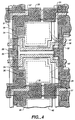
- Fig. 4 is a plan view showing an example of a pixel portion of the liquid crystal display device of Fig. 1.
- a TFT 34 is arranged at the crossing point between a signal line 31 and a scanning line 32.
- a semiconductor thin film 33 forms the source, drain and channel of TFT 34.
- Numeral 35 designates a contact hole for commonly connecting the source of a pair of TFTs for upper and lower pixels with the signal line 31.
- Numeral 36 designates a contact hole for connecting the drain of TFT 34 with a pixel electrode 39.
- a storage capacitor 38 is formed between the drain of TFT 34 and a common electrode 37.
- the common electrode 37 is used for the storage capacitors of a pair of pixels positioned on opposite sides of the common electrode.
- the portion indicated in aperture 40 becomes an effective region for image display. Since those regions other than the aperture 40 adversely affect the image quality, they are covered with a light shield to avoid the permeation of light.
- the common electrode 37 is arranged in the region between the pixel electrodes which is not necessary for the image display, a high aperture ratio can be obtained.
- the area of the aperture 40 in Fig. 4 is larger than that of the aperture 30 in Fig. 3 by about 30%.
- the image plane can be brighter by 30% as compared with a similar element with a similar pixel pitch.
- the form of the aperture is changed from rectangular to approximately square, the lattice-like structure of the light shield layer becomes less apparent, remarkably improving the image quality. Further, if a slanted wiring pattern is used, it is possible to make the aperture ideally circular.
- NTSC and HDTV signals are provided with two interlaced fields.
- a driving method is often used in which two adjacent scanning lines are formed as a pair to be selected by the same timing to be written with the same data, and the pairs are changed every field.
- the color phosphor arrangement may be of the mosaic or triangular type.
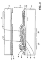
- Fig. 5 is a cross-sectional view of an example of a liquid crystal display device corresponding to Fig. 4 and Fig. 3.
- the liquid crystal display device using TFTs has two insulative substrates, i.e. the liquid crystal 43 is interposed between a TFT substrate 41 and a counter substrate 42.
- the TFTs 34 and the storage capacitors 38 are arranged on the TFT substrate 41 .
- the structure as shown in this Figure is of the coplanar type, in which the source 47 of the TFT, the drain 49 and the channel 48 are formed in the same semiconductor film. Since impurities are doped into the source 47 and the drain 49 from a gate insulative film 50 using the gate electrode 46 as a mask, the TFTs are of the self-alignment type.
- the storage capacitor 38 is formed as a MOS capacitor between the common electrode 37 and the drain 49, the common electrode 37 being formed of the same film as the gate electrode 46 of the TFT 34.
- MOS capacitor There are two methods for forming a MOS capacitor. One method is to dope the semiconductor film with impurities before forming the gate electrode 46 and the common electrode 37. In this case, the electric potential of the common electrode 37 can be selected freely. In the second method, no special doping with impurities is performed. In this case, since the semiconductor thin film under the common electrode 37 becomes similar to the channel 48, a bias allowing formation of a reversed layer on the channel must be supplied to the common electrode 37 to use the MOS capacitance.
- the signal line 31 and the pixel electrode 39 are respectively connected to the source 47 and the drain 49 of the TFT 34 through contact holes.
- an additional storage capacitor is formed between the pixel electrode 39 and the common electrode 37 through an interlayer insulating film 54.
- a layer of high precision and little defects such as a thermal oxide film, is used for the gate insulating film, and it is formed rather thin to obtain excellent electric characteristics of the TFT. Therefore, the MOS capacitor mentioned above can have several times the capacitance of the capacitor formed between the common electrode 37 and the pixel electrode 39.
- the drain 49 of the TFT and the contact hole of the pixel electrode 39 are arranged on the right side of the common electrode 37, only the MOS capacitor provides the function of the storage capacitor 38.
- a passivation film 55 protects the thin film element and blocks a direct current flow through the liquid crystal.
- a light shield layer 56 provided on the counter substrate 42 controls a light leakage electric current of the TFT and results in high quality images having a large contrast ratio by covering non-effective portions of the image display.
- the aperture 40 is the effective region for the image display.
- the counter electrode 57 is made of a transparent electrically conductive film and covers all the surfaces contacting the liquid crystal.
- the liquid crystal 43 is driven by the electric field formed between the pixel electrode 39 and the counter electrode 57.
- the pixel electrode 39 is formed by a transparent electrically conductive film, and if it is used as a reflection type-display device, the pixel electrode 39 is formed by a metallic thin film.
- Fig. 6 shows a plan view of a pixel portion according to a second embodiment of the invention.
- the TFT is arranged at a crossing point between the signal line 61 and the scanning line 62.
- the source 65 and the drain 66 of the TFT are formed in a semiconductor thin film layer different from that (63) of the channel 64.
- the common electrode 67 is used for the storage capacitors 68 of the pixels positioned on both sides of this common electrode.
- the pixel electrode 69 is connected with both, the drain 66 of the TFT and the storage capacitor 68.
- the region of the aperture 70 is the effective region for the image display. Since the region excepting the aperture 70 can degrade the image, they are covered with a light shield layer for preventing the permeation of light.
- Fig. 7 is an example of a cross-sectional view of the liquid crystal display device corresponding to Fig. 6.
- the liquid crystal display device of this embodiment is also provided with a liquid crystal 73 between a pair of insulative substrates, namely between the TFT substrate 71 and the counter substrate 72.
- the elements comprising the TFT 74 and the storage capacitor 68.
- the TFT shown in this Figure is of the "reverse stagger" type, having a gate electrode 76, a gate insulation film 80, a semiconductor thin film 78 forming the channel and an impurity containing semiconductor thin film 88, which are superposed one upon the other.
- a source electrode 77 and a drain electrode 79 are formed on the impurity containing semiconductor thin film 88.
- the source electrode 77 is formed by diverging from the signal line and the drain electrode is connected to the pixel electrode 69.
- a "stagger" type could be used which corresponds to the reverse stagger type shown in Fig. 7 turned upside down, i.e. with the order of layers being just contrary to that shown in Fig. 7.
- the storage capacitor 68 has a similar structure to that of the drain of the TFT, being arranged on the common electrode 67 and connected to the pixel electrode 69.
- the passivation layer 84 protects the thin film element and cuts the direct current applied to the liquid crystal.
- the light shield layer 85 arranged on the counter substrate 72 controls the light leakage electric current of the TFT and results in high quality images having a large contrast ratio by covering non-effective portions of the image display.
- the aperture 70 is the effective region for the image display.
- the counter electrode 86 made of a transparent electrically conductive film covers all surfaces contacting the liquid crystal, and the liquid crystal 73 is driven by the electric field between the pixel electrode 69 and the counter electrode 86.
- Fig. 8 is a plan view showing another embodiment of a pixel portion in a liquid crystal display device according to the invention.
- the pixel arrangement as shown herein is of the so-called triangular type often used in the video field because the pixel pattern is hardly perceivable.
- the TFT is arranged at a crossing point between signal line 111 and scanning line 112.
- the signal line 111 has a square wave or meander-like pattern as shown in Fig. 8.
- the source 105 and the drain 106 of the TFT are formed from a thin film layer different from that (98) of the channel 104.
- the signal line 111 overlies the source 105.
- the common electrode 101 overlies a partial portion of a pair of pixel electrodes 102 adjacent thereto.
- Numeral 90 is the aperture which is the effective area for the image display, 95 the storage capacitor.
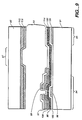
- Fig. 9 represents a cross-sectional view of a liquid crystal display device corresponding to Fig. 8.
- the liquid crystal display device of this embodiment is also provided with a liquid crystal 93 between a pair of insulative substrates, namely between the TFT substrate 91 and the counter substrate 92.
- the elements comprising TFTs 94 and a storage capacitors 95.
- the TFT as shown in this Figure is of the "reverse stagger" type, which is provided with a gate insulation film 100 on a gate electrode 96, a semiconductor thin film 98 forming the channel and the impurity containing semiconductor thin film 108 which are superposed serially.
- a source electrode 97 and a drain electrode 99 are formed on the impurity containing semiconductor thin film 108, the source electrode 97 being a part of the signal line and the drain electrode 99 being connected to the pixel electrode 102.
- the storage capacitor (95) is formed by superposing the pixel electrode 102 over the common electrode 101 through the gate insulation film 100.
- Numeral 114 designates the passivation film.
- Numeral 115 designates the light shield layer, and numeral 116 designates the counter electrode formed by a transparent electrically conductive film.
Landscapes
- Physics & Mathematics (AREA)
- Engineering & Computer Science (AREA)
- Chemical & Material Sciences (AREA)
- Crystallography & Structural Chemistry (AREA)
- Nonlinear Science (AREA)
- General Physics & Mathematics (AREA)
- Theoretical Computer Science (AREA)
- Power Engineering (AREA)
- Microelectronics & Electronic Packaging (AREA)
- Mathematical Physics (AREA)
- Computer Hardware Design (AREA)
- Optics & Photonics (AREA)
- Liquid Crystal (AREA)
- Liquid Crystal Display Device Control (AREA)
Claims (4)
- Flüssigkristallanzeigevorrichtung, umfassend:
ein erstes isolierendes Substrat (41, 91), auf dem sich eine Vielzahl von Signalleitungen (31, 61, 111), eine Vielzahl von die Signalleitungen kreuzenden Abtastleitungen (32, 62, 112), eine Vielzahl von Dünnfilmtransistoren (34, 64, 104), die an den Kreuzungspunkten zwischen den Signalleitungen und den Abtastleitungen vorgesehen sind, eine Vielzahl von Pixelelektroden (39, 69, 102), die jeweils mit den Dünnfilmtransistoren verbunden sind, und eine Vielzahl von Speicherkondensatoren (38, 68, 95) befinden, die den Pixelelektroden jeweils zugeordnet sind, wobei die den Pixelelektroden zugeordneten und mit einer jeweiligen Abtastleitung verbundenen Speicherkondensatoren von einer gemeinsamen Elektrode (37, 67, 101), die sich zwischen zwei Abtastleitungen erstreckt, gebildet und zusammengeschaltet werden;
ein zweites isolierendes Substrat (42, 72, 92), auf dem sich eine Elektrode (57, 86, 116) befindet; und
einen Flüssigkristall (43, 73, 93), der in dem zwischen dem ersten und dem zweiten isolierenden Substrat gebildeten Raum angeordnet ist;
dadurch gekennzeichnet, daß zwischen jeder Abtastleitung einer ungeradzahligen/geradzahligen Nummer und der Abtastleitung der folgenden geradzahligen/ungeradzahligen Nummer zwei Anordnungen von Pixelelektroden, in der Richtung der Signalleitungen benachbart, plaziert sind, von denen eine mit der Abtastleitung der ungeradzahligen/geradzahligen Nummer verbunden ist, während die andere mit der Abtastleitung der folgenden geradzahligen/ungeradzahligen Nummer verbunden ist, wobei eine gemeinsame Elektrode zur Bildung und zum Zusammenschalten der den beiden Anordnungen von Pixelelektroden zugeordneten Speicherkondensatoren angeordnet ist, und
dadurch, daß jede Abtastleitung mit einer geradzahligen/ungeradzahligen Nummer und die Abtastleitung mit der folgenden ungeradzahligen/geradzahligen Nummer nebeneinander angeordnet sind, ohne daß eine gemeinsame Elektrode dazwischen gesetzt ist. - Flüssigkristallanzeigevorrichtung nach Anspruch 1, bei der ein gemeinsamer Verbindungspunkt (35) zwischen einer jeweiligen Signalleitung (31) und den Sourcen eines Paares der Dünnfilmtransistoren (34, 64, 104), die einer geradzahligen/ungeradzahligen Abtastleitung (32) bzw. der folgenden ungeradzahligen/geradzahligen Abtastleitung zugeordnet sind, vorgesehen ist.
- Flüssigkristallanzeigevorrichtung nach Anspruch 1 oder 2, bei der die gemeinsame Elektrode (101) so angeordnet ist, daß sie wenigstens einen Abschnitt der Pixelelektroden (102) bedeckt, welche einer ungeradzahligen/geradzahligen Abtastleitung (112) zugeordnet sind, und solchen, die der nächsten geradzahligen/ungeradzahligen Abtastleitung zugeordnet sind.
- Flüssigkristallanzeigevorrichtung nach einem der Ansprüche 1 bis 3 verwendet in Verbindung mit einem Ansteuerungsverfahren, bei dem die Anzeige mit zwei Zeilensprungsignalhalbbildern versehen ist, so daß ein Paar benachbarter Abtastleitungen gleichzeitig ausgewählt wird und mit demselben Signal beschrieben wird, wobei das in das Paar Abtastleitungen in einem ungeradzahligen Halbbild geschriebene Signal verschieden von dem in einem geradzahligen Halbbild ist.
Applications Claiming Priority (2)
| Application Number | Priority Date | Filing Date | Title |
|---|---|---|---|
| JP32503789A JP2714993B2 (ja) | 1989-12-15 | 1989-12-15 | 液晶表示装置 |
| JP325037/89 | 1989-12-15 |
Publications (2)
| Publication Number | Publication Date |
|---|---|
| EP0435101A1 EP0435101A1 (de) | 1991-07-03 |
| EP0435101B1 true EP0435101B1 (de) | 1994-12-07 |
Family
ID=18172445
Family Applications (1)
| Application Number | Title | Priority Date | Filing Date |
|---|---|---|---|
| EP90124155A Expired - Lifetime EP0435101B1 (de) | 1989-12-15 | 1990-12-13 | Flüssigkristall-Anzeigevorrichtung in Matrixform mit Dünnschichttransistoren |
Country Status (4)
| Country | Link |
|---|---|
| US (1) | US5247289A (de) |
| EP (1) | EP0435101B1 (de) |
| JP (1) | JP2714993B2 (de) |
| DE (1) | DE69014842T2 (de) |
Families Citing this family (71)
| Publication number | Priority date | Publication date | Assignee | Title |
|---|---|---|---|---|
| US6556257B2 (en) * | 1991-09-05 | 2003-04-29 | Sony Corporation | Liquid crystal display device |
| KR940004322B1 (ko) * | 1991-09-05 | 1994-05-19 | 삼성전자 주식회사 | 액정표시장치 및 그 제조방법 |
| US5457553A (en) * | 1991-12-25 | 1995-10-10 | Casio Computer Co., Ltd. | Thin-film transistor panel with reduced number of capacitor lines |
| JP3172841B2 (ja) * | 1992-02-19 | 2001-06-04 | 株式会社日立製作所 | 薄膜トランジスタとその製造方法及び液晶表示装置 |
| US5576857A (en) * | 1992-04-02 | 1996-11-19 | Semiconductor Energy Laboratory Co., Ltd. | Electro-optical device with transistors and capacitors method of driving the same |
| EP0592063A3 (en) * | 1992-09-14 | 1994-07-13 | Toshiba Kk | Active matrix liquid crystal display device |
| US5715025A (en) * | 1993-02-22 | 1998-02-03 | Goldstar Co., Ltd. | Active matrix for liquid crystal displays in which a data bus consists of two data subbuses and each data subbus is separated from an adjacent data bus by one display electrode |
| GB2308218B (en) * | 1993-03-04 | 1997-08-20 | Samsung Electronics Co Ltd | Liquid crystal display and method for manufacturing the same |
| FR2702286B1 (fr) * | 1993-03-04 | 1998-01-30 | Samsung Electronics Co Ltd | Affichage à cristaux liquides et procédé pour le fabriquer. |
| JPH06313876A (ja) * | 1993-04-28 | 1994-11-08 | Canon Inc | 液晶表示装置の駆動方法 |
| EP0863498B1 (de) * | 1993-08-30 | 2002-10-23 | Sharp Kabushiki Kaisha | Datensignalleitungsstruktur in einer Flüssigkristall-Anzeigeeinrichtung mit aktiver Matrix |
| US5719065A (en) | 1993-10-01 | 1998-02-17 | Semiconductor Energy Laboratory Co., Ltd. | Method for manufacturing semiconductor device with removable spacers |
| US5600459A (en) * | 1993-12-20 | 1997-02-04 | Roy; Howard S. | Multiple-shutter flat-panel display having individually controlled pixels and method for making same |
| US5486485A (en) * | 1994-02-18 | 1996-01-23 | Philip Electronics North America Corporation | Method of manufacturing a reflective display |
| US5491347A (en) * | 1994-04-28 | 1996-02-13 | Xerox Corporation | Thin-film structure with dense array of binary control units for presenting images |
| US5814529A (en) | 1995-01-17 | 1998-09-29 | Semiconductor Energy Laboratory Co., Ltd. | Method for producing a semiconductor integrated circuit including a thin film transistor and a capacitor |
| US5774099A (en) * | 1995-04-25 | 1998-06-30 | Hitachi, Ltd. | Liquid crystal device with wide viewing angle characteristics |
| JP3304706B2 (ja) * | 1995-09-20 | 2002-07-22 | ソニー株式会社 | アクティブマトリクス表示装置 |
| JPH09236826A (ja) * | 1995-09-28 | 1997-09-09 | Sharp Corp | 液晶表示素子およびその製造方法 |
| KR100234402B1 (ko) * | 1996-01-19 | 1999-12-15 | 윤종용 | 액정 표시 장치의 구동 방법 및 장치 |
| US5790090A (en) * | 1996-10-16 | 1998-08-04 | International Business Machines Corporation | Active matrix liquid crystal display with reduced drive pulse amplitudes |
| JPH10186399A (ja) * | 1996-12-20 | 1998-07-14 | Sony Corp | 液晶装置 |
| US6256076B1 (en) * | 1997-03-19 | 2001-07-03 | Samsung Electronics Co., Ltd. | Liquid crystal displays having switching elements and storage capacitors and a manufacturing method thereof |
| US5999234A (en) * | 1997-04-15 | 1999-12-07 | International Business Machines Corporation | Transmissive cell for ultra small pixel applications |
| JP4271268B2 (ja) | 1997-09-20 | 2009-06-03 | 株式会社半導体エネルギー研究所 | イメージセンサおよびイメージセンサ一体型アクティブマトリクス型表示装置 |
| KR100293808B1 (ko) | 1997-12-17 | 2001-10-24 | 박종섭 | 색띰방지용액정표시장치 |
| JPH11326954A (ja) * | 1998-05-15 | 1999-11-26 | Semiconductor Energy Lab Co Ltd | 半導体装置 |
| JP4070896B2 (ja) * | 1998-10-07 | 2008-04-02 | 三菱電機株式会社 | 電気光学素子および該電気光学素子の製造方法 |
| US6140990A (en) * | 1998-10-16 | 2000-10-31 | International Business Machines Corporation | Active matrix liquid crystal display incorporating pixel inversion with reduced drive pulse amplitudes |
| KR100430232B1 (ko) * | 1998-12-21 | 2004-12-31 | 엘지.필립스 엘시디 주식회사 | 액정표시장치및액정표시장치의축적캐패시터 |
| US6437839B1 (en) | 1999-04-23 | 2002-08-20 | National Semiconductor Company | Liquid crystal on silicon (LCOS) display pixel with multiple storage capacitors |
| KR100709704B1 (ko) * | 2000-05-12 | 2007-04-19 | 삼성전자주식회사 | 액정 표시 장치용 박막 트랜지스터 기판 및 그 제조 방법 |
| TWI288909B (en) * | 2000-07-19 | 2007-10-21 | Toshiba Matsushita Display Tec | Liquid crystal display |
| KR100391157B1 (ko) | 2001-10-25 | 2003-07-16 | 엘지.필립스 엘시디 주식회사 | 액정 표시 장치용 어레이 기판 및 그의 제조 방법 |
| JP4008716B2 (ja) * | 2002-02-06 | 2007-11-14 | シャープ株式会社 | フラットパネル表示装置およびその製造方法 |
| US7038239B2 (en) | 2002-04-09 | 2006-05-02 | Semiconductor Energy Laboratory Co., Ltd. | Semiconductor element and display device using the same |
| JP3989761B2 (ja) | 2002-04-09 | 2007-10-10 | 株式会社半導体エネルギー研究所 | 半導体表示装置 |
| TWI270919B (en) | 2002-04-15 | 2007-01-11 | Semiconductor Energy Lab | Display device and method of fabricating the same |
| JP3989763B2 (ja) | 2002-04-15 | 2007-10-10 | 株式会社半導体エネルギー研究所 | 半導体表示装置 |
| US7256421B2 (en) | 2002-05-17 | 2007-08-14 | Semiconductor Energy Laboratory, Co., Ltd. | Display device having a structure for preventing the deterioration of a light emitting device |
| US7116319B2 (en) * | 2002-05-21 | 2006-10-03 | Canon Kabushiki Kaisha | Image forming apparatus and radiation detection system |
| TWI226482B (en) * | 2003-02-18 | 2005-01-11 | Hannstar Display Corp | Liquid crystal display panel and its driving method |
| JP4216270B2 (ja) | 2004-06-30 | 2009-01-28 | 三星エスディアイ株式会社 | 電子装置、薄膜トランジスタ構造体及びそれを備える平板ディスプレイ装置 |
| KR100626009B1 (ko) * | 2004-06-30 | 2006-09-20 | 삼성에스디아이 주식회사 | 박막 트랜지스터 구조체 및 이를 구비하는 평판디스플레이 장치 |
| KR100563067B1 (ko) * | 2004-06-30 | 2006-03-24 | 삼성에스디아이 주식회사 | 박막 트랜지스터 구조체 및 이를 구비하는 평판디스플레이 장치 |
| KR20060111265A (ko) * | 2005-04-22 | 2006-10-26 | 삼성전자주식회사 | 박막 트랜지스터 기판, 이의 제조 방법 및 이를 갖는 표시장치 |
| US8212953B2 (en) | 2005-12-26 | 2012-07-03 | Semiconductor Energy Laboratory Co., Ltd. | Semiconductor device and method for manufacturing the same |
| JP4954548B2 (ja) * | 2005-12-28 | 2012-06-20 | ティーピーオー、ホンコン、ホールディング、リミテッド | 液晶表示装置およびその制御方法 |
| KR101337256B1 (ko) * | 2007-02-14 | 2013-12-05 | 삼성디스플레이 주식회사 | 표시 장치의 구동 장치 및 이를 포함하는 표시 장치 |
| JP5194494B2 (ja) * | 2007-03-12 | 2013-05-08 | コニカミノルタホールディングス株式会社 | 画素アレイ |
| JP5162952B2 (ja) * | 2007-04-26 | 2013-03-13 | 日本電気株式会社 | 液晶表示装置用反射板の製造方法、液晶表示装置及び液晶表示装置用アレイ基板 |
| CN101382679B (zh) * | 2007-09-07 | 2012-02-08 | 群康科技(深圳)有限公司 | 液晶显示面板 |
| US20100231493A1 (en) * | 2007-09-27 | 2010-09-16 | Yasuyoshi Kaise | Display device |
| US8610653B2 (en) | 2007-10-11 | 2013-12-17 | Sharp Kabushiki Kaisha | Liquid crystal display panel and liquid crystal display device |
| US20100328198A1 (en) * | 2008-02-27 | 2010-12-30 | Toshihide Tsubata | Active matrix substrate, liquid crystal panel, liquid crystal display device, liquid crystal display unit, and television receiver |
| KR101529288B1 (ko) | 2008-04-17 | 2015-06-17 | 삼성디스플레이 주식회사 | 표시장치 |
| US8816350B2 (en) | 2009-03-13 | 2014-08-26 | Sharp Kabushiki Kaisha | Array substrate, liquid crystal panel, liquid crystal display device, and television receiver |
| JP5573540B2 (ja) * | 2010-09-22 | 2014-08-20 | カシオ計算機株式会社 | タッチパネル |
| JP5958055B2 (ja) * | 2011-07-29 | 2016-07-27 | セイコーエプソン株式会社 | 電気光学装置、電気光学装置の駆動方法および電子機器 |
| KR101922088B1 (ko) * | 2012-05-23 | 2018-11-27 | 삼성디스플레이 주식회사 | 액정 표시 장치 |
| US20140014948A1 (en) * | 2012-07-12 | 2014-01-16 | Semiconductor Energy Laboratory Co. Ltd. | Semiconductor device |
| JP2012252361A (ja) * | 2012-08-29 | 2012-12-20 | Semiconductor Energy Lab Co Ltd | 表示装置 |
| JP5482851B2 (ja) * | 2012-09-07 | 2014-05-07 | コニカミノルタ株式会社 | 画素アレイ |
| CN103018987B (zh) * | 2012-12-06 | 2015-05-13 | 京东方科技集团股份有限公司 | 阵列基板及显示装置 |
| CN103021369A (zh) * | 2012-12-21 | 2013-04-03 | 北京京东方光电科技有限公司 | 液晶显示器的驱动方法 |
| US10642116B2 (en) | 2013-05-01 | 2020-05-05 | Apple Inc. | Display pixels with improved storage capacitance |
| KR20140144958A (ko) * | 2013-06-12 | 2014-12-22 | 삼성디스플레이 주식회사 | 액정 변조기 및 이를 포함하는 검사 장치 |
| KR102216659B1 (ko) * | 2014-07-15 | 2021-02-18 | 엘지디스플레이 주식회사 | 액정표시장치의 픽셀 어레이 |
| CN104597671B (zh) | 2015-01-22 | 2018-07-27 | 厦门天马微电子有限公司 | 阵列基板、显示面板及显示装置 |
| KR102584437B1 (ko) * | 2018-07-24 | 2023-09-27 | 엘지디스플레이 주식회사 | 표시장치 |
| CN113741109A (zh) * | 2021-09-08 | 2021-12-03 | Tcl华星光电技术有限公司 | 阵列基板及显示面板 |
Family Cites Families (10)
| Publication number | Priority date | Publication date | Assignee | Title |
|---|---|---|---|---|
| DE3019832C2 (de) * | 1979-05-28 | 1986-10-16 | Kabushiki Kaisha Suwa Seikosha, Shinjuku, Tokio/Tokyo | Treiberschaltung für eine Flüssigkristallanzeigematrix |
| US4431271A (en) * | 1979-09-06 | 1984-02-14 | Canon Kabushiki Kaisha | Display device with a thin film transistor and storage condenser |
| JPH0697317B2 (ja) * | 1984-04-11 | 1994-11-30 | ホシデン株式会社 | 液晶表示器 |
| WO1986001624A1 (fr) * | 1984-08-23 | 1986-03-13 | Sony Corporation | Affichage a cristaux liquides |
| JPH0750381B2 (ja) * | 1984-12-20 | 1995-05-31 | キヤノン株式会社 | カラー液晶表示装置 |
| EP0287055B1 (de) * | 1987-04-15 | 1993-09-29 | Sharp Kabushiki Kaisha | Flüssigkristallanzeigegerät |
| JP2613209B2 (ja) * | 1987-05-01 | 1997-05-21 | 旭硝子株式会社 | 画像表示装置 |
| JPS6473324A (en) * | 1987-09-14 | 1989-03-17 | Matsushita Electric Industrial Co Ltd | Display device and its driving method |
| DE68917774T2 (de) * | 1988-04-30 | 1995-03-16 | Sharp Kk | Dünnfilm-Halbleitervorrichtung und damit hergestellte Flüssigkristallanzeige. |
| EP0376329B1 (de) * | 1988-12-28 | 1995-03-08 | Sony Corporation | Flüssigkristall-Anzeigevorrichtung |
-
1989
- 1989-12-15 JP JP32503789A patent/JP2714993B2/ja not_active Expired - Fee Related
-
1990
- 1990-12-13 DE DE69014842T patent/DE69014842T2/de not_active Expired - Fee Related
- 1990-12-13 EP EP90124155A patent/EP0435101B1/de not_active Expired - Lifetime
- 1990-12-14 US US07/628,917 patent/US5247289A/en not_active Expired - Lifetime
Also Published As
| Publication number | Publication date |
|---|---|
| DE69014842T2 (de) | 1995-05-11 |
| US5247289A (en) | 1993-09-21 |
| EP0435101A1 (de) | 1991-07-03 |
| JPH03185428A (ja) | 1991-08-13 |
| DE69014842D1 (de) | 1995-01-19 |
| JP2714993B2 (ja) | 1998-02-16 |
Similar Documents
| Publication | Publication Date | Title |
|---|---|---|
| EP0435101B1 (de) | Flüssigkristall-Anzeigevorrichtung in Matrixform mit Dünnschichttransistoren | |
| CN1321342C (zh) | 液晶显示器 | |
| JP3349935B2 (ja) | アクティブマトリクス型液晶表示装置 | |
| EP0244013B1 (de) | Farbwiedergabevorrichtung | |
| US5446562A (en) | Liquid crystal display device with transparent conductive film between pixel electrodes and signal or scanning lines | |
| KR100596143B1 (ko) | 액정 표시 장치 및 그 제조 방법 | |
| EP0661581B1 (de) | Flüssigkristall-Anzeigevorrichtung mit aktiver Matrix | |
| EP0389031A1 (de) | Wiedergabeanordnung für Farbwiedergabe | |
| US6064454A (en) | Color filter panel of an LCD device | |
| EP0689086B1 (de) | Anzeigevorrichtung | |
| KR0144061B1 (ko) | 실드된 픽셀 구조를 갖는 액정 디스플레이 장치 | |
| EP0554061B1 (de) | Flüssigkristallanzeige | |
| JP3050175B2 (ja) | 表示装置 | |
| JP4356135B2 (ja) | カラー表示装置 | |
| KR20030086157A (ko) | 액정 표시 장치 | |
| JP2947233B2 (ja) | 表示装置 | |
| JPH0744669B2 (ja) | 液晶表示装置 | |
| JP2541446B2 (ja) | アクティブマトリックスパネル | |
| JPH0627982B2 (ja) | 表示装置 | |
| JP3036059B2 (ja) | 液晶表示装置 | |
| JPS6057371A (ja) | 液晶ビデオ表示装置 | |
| JPH02132419A (ja) | フルライン液晶表示装置 | |
| JP3793865B2 (ja) | 液晶表示装置 | |
| JPH07128687A (ja) | アクティブマトリックス型パネル装置 | |
| JPH0570154B2 (de) |
Legal Events
| Date | Code | Title | Description |
|---|---|---|---|
| PUAI | Public reference made under article 153(3) epc to a published international application that has entered the european phase |
Free format text: ORIGINAL CODE: 0009012 |
|
| AK | Designated contracting states |
Kind code of ref document: A1 Designated state(s): DE FR GB NL |
|
| 17P | Request for examination filed |
Effective date: 19911126 |
|
| 17Q | First examination report despatched |
Effective date: 19930503 |
|
| GRAA | (expected) grant |
Free format text: ORIGINAL CODE: 0009210 |
|
| AK | Designated contracting states |
Kind code of ref document: B1 Designated state(s): DE FR GB NL |
|
| REF | Corresponds to: |
Ref document number: 69014842 Country of ref document: DE Date of ref document: 19950119 |
|
| ET | Fr: translation filed | ||
| PLBE | No opposition filed within time limit |
Free format text: ORIGINAL CODE: 0009261 |
|
| STAA | Information on the status of an ep patent application or granted ep patent |
Free format text: STATUS: NO OPPOSITION FILED WITHIN TIME LIMIT |
|
| 26N | No opposition filed | ||
| REG | Reference to a national code |
Ref country code: GB Ref legal event code: IF02 |
|
| PGFP | Annual fee paid to national office [announced via postgrant information from national office to epo] |
Ref country code: NL Payment date: 20061217 Year of fee payment: 17 |
|
| PGFP | Annual fee paid to national office [announced via postgrant information from national office to epo] |
Ref country code: GB Payment date: 20071212 Year of fee payment: 18 Ref country code: FR Payment date: 20071210 Year of fee payment: 18 |
|
| PGFP | Annual fee paid to national office [announced via postgrant information from national office to epo] |
Ref country code: DE Payment date: 20071206 Year of fee payment: 18 |
|
| NLV4 | Nl: lapsed or anulled due to non-payment of the annual fee |
Effective date: 20080701 |
|
| PG25 | Lapsed in a contracting state [announced via postgrant information from national office to epo] |
Ref country code: NL Free format text: LAPSE BECAUSE OF NON-PAYMENT OF DUE FEES Effective date: 20080701 |
|
| GBPC | Gb: european patent ceased through non-payment of renewal fee |
Effective date: 20081213 |
|
| REG | Reference to a national code |
Ref country code: FR Ref legal event code: ST Effective date: 20090831 |
|
| PG25 | Lapsed in a contracting state [announced via postgrant information from national office to epo] |
Ref country code: DE Free format text: LAPSE BECAUSE OF NON-PAYMENT OF DUE FEES Effective date: 20090701 |
|
| PG25 | Lapsed in a contracting state [announced via postgrant information from national office to epo] |
Ref country code: GB Free format text: LAPSE BECAUSE OF NON-PAYMENT OF DUE FEES Effective date: 20081213 |
|
| PG25 | Lapsed in a contracting state [announced via postgrant information from national office to epo] |
Ref country code: FR Free format text: LAPSE BECAUSE OF NON-PAYMENT OF DUE FEES Effective date: 20081231 |