EP0435187A2 - Verfahren zur Herstellung einer Halbleitervorrichtung - Google Patents
Verfahren zur Herstellung einer Halbleitervorrichtung Download PDFInfo
- Publication number
- EP0435187A2 EP0435187A2 EP90125081A EP90125081A EP0435187A2 EP 0435187 A2 EP0435187 A2 EP 0435187A2 EP 90125081 A EP90125081 A EP 90125081A EP 90125081 A EP90125081 A EP 90125081A EP 0435187 A2 EP0435187 A2 EP 0435187A2
- Authority
- EP
- European Patent Office
- Prior art keywords
- insulating film
- opening portion
- film
- lower layer
- layer insulating
- Prior art date
- Legal status (The legal status is an assumption and is not a legal conclusion. Google has not performed a legal analysis and makes no representation as to the accuracy of the status listed.)
- Withdrawn
Links
Images





Classifications
-
- H—ELECTRICITY
- H10—SEMICONDUCTOR DEVICES; ELECTRIC SOLID-STATE DEVICES NOT OTHERWISE PROVIDED FOR
- H10W—GENERIC PACKAGES, INTERCONNECTIONS, CONNECTORS OR OTHER CONSTRUCTIONAL DETAILS OF DEVICES COVERED BY CLASS H10
- H10W20/00—Interconnections in chips, wafers or substrates
- H10W20/01—Manufacture or treatment
- H10W20/031—Manufacture or treatment of conductive parts of the interconnections
- H10W20/056—Manufacture or treatment of conductive parts of the interconnections by filling conductive material into holes, grooves or trenches
- H10W20/059—Manufacture or treatment of conductive parts of the interconnections by filling conductive material into holes, grooves or trenches by reflowing or applying pressure
-
- H—ELECTRICITY
- H10—SEMICONDUCTOR DEVICES; ELECTRIC SOLID-STATE DEVICES NOT OTHERWISE PROVIDED FOR
- H10W—GENERIC PACKAGES, INTERCONNECTIONS, CONNECTORS OR OTHER CONSTRUCTIONAL DETAILS OF DEVICES COVERED BY CLASS H10
- H10W20/00—Interconnections in chips, wafers or substrates
- H10W20/01—Manufacture or treatment
- H10W20/031—Manufacture or treatment of conductive parts of the interconnections
-
- H—ELECTRICITY
- H10—SEMICONDUCTOR DEVICES; ELECTRIC SOLID-STATE DEVICES NOT OTHERWISE PROVIDED FOR
- H10P—GENERIC PROCESSES OR APPARATUS FOR THE MANUFACTURE OR TREATMENT OF DEVICES COVERED BY CLASS H10
- H10P50/00—Etching of wafers, substrates or parts of devices
- H10P50/20—Dry etching; Plasma etching; Reactive-ion etching
- H10P50/28—Dry etching; Plasma etching; Reactive-ion etching of insulating materials
- H10P50/282—Dry etching; Plasma etching; Reactive-ion etching of insulating materials of inorganic materials
- H10P50/283—Dry etching; Plasma etching; Reactive-ion etching of insulating materials of inorganic materials by chemical means
-
- H—ELECTRICITY
- H10—SEMICONDUCTOR DEVICES; ELECTRIC SOLID-STATE DEVICES NOT OTHERWISE PROVIDED FOR
- H10P—GENERIC PROCESSES OR APPARATUS FOR THE MANUFACTURE OR TREATMENT OF DEVICES COVERED BY CLASS H10
- H10P76/00—Manufacture or treatment of masks on semiconductor bodies, e.g. by lithography or photolithography
- H10P76/20—Manufacture or treatment of masks on semiconductor bodies, e.g. by lithography or photolithography of masks comprising organic materials
- H10P76/204—Manufacture or treatment of masks on semiconductor bodies, e.g. by lithography or photolithography of masks comprising organic materials of organic photoresist masks
- H10P76/2041—Photolithographic processes
- H10P76/2042—Photolithographic processes using lasers
-
- H—ELECTRICITY
- H10—SEMICONDUCTOR DEVICES; ELECTRIC SOLID-STATE DEVICES NOT OTHERWISE PROVIDED FOR
- H10P—GENERIC PROCESSES OR APPARATUS FOR THE MANUFACTURE OR TREATMENT OF DEVICES COVERED BY CLASS H10
- H10P95/00—Generic processes or apparatus for manufacture or treatments not covered by the other groups of this subclass
-
- H—ELECTRICITY
- H10—SEMICONDUCTOR DEVICES; ELECTRIC SOLID-STATE DEVICES NOT OTHERWISE PROVIDED FOR
- H10W—GENERIC PACKAGES, INTERCONNECTIONS, CONNECTORS OR OTHER CONSTRUCTIONAL DETAILS OF DEVICES COVERED BY CLASS H10
- H10W20/00—Interconnections in chips, wafers or substrates
- H10W20/01—Manufacture or treatment
- H10W20/031—Manufacture or treatment of conductive parts of the interconnections
- H10W20/056—Manufacture or treatment of conductive parts of the interconnections by filling conductive material into holes, grooves or trenches
-
- H—ELECTRICITY
- H10—SEMICONDUCTOR DEVICES; ELECTRIC SOLID-STATE DEVICES NOT OTHERWISE PROVIDED FOR
- H10W—GENERIC PACKAGES, INTERCONNECTIONS, CONNECTORS OR OTHER CONSTRUCTIONAL DETAILS OF DEVICES COVERED BY CLASS H10
- H10W20/00—Interconnections in chips, wafers or substrates
- H10W20/01—Manufacture or treatment
- H10W20/071—Manufacture or treatment of dielectric parts thereof
- H10W20/074—Manufacture or treatment of dielectric parts thereof of dielectric parts comprising thin functional dielectric layers, e.g. dielectric etch-stop, barrier, capping or liner layers
-
- H—ELECTRICITY
- H10—SEMICONDUCTOR DEVICES; ELECTRIC SOLID-STATE DEVICES NOT OTHERWISE PROVIDED FOR
- H10W—GENERIC PACKAGES, INTERCONNECTIONS, CONNECTORS OR OTHER CONSTRUCTIONAL DETAILS OF DEVICES COVERED BY CLASS H10
- H10W20/00—Interconnections in chips, wafers or substrates
- H10W20/01—Manufacture or treatment
- H10W20/071—Manufacture or treatment of dielectric parts thereof
- H10W20/074—Manufacture or treatment of dielectric parts thereof of dielectric parts comprising thin functional dielectric layers, e.g. dielectric etch-stop, barrier, capping or liner layers
- H10W20/076—Manufacture or treatment of dielectric parts thereof of dielectric parts comprising thin functional dielectric layers, e.g. dielectric etch-stop, barrier, capping or liner layers in via holes or trenches
-
- H—ELECTRICITY
- H10—SEMICONDUCTOR DEVICES; ELECTRIC SOLID-STATE DEVICES NOT OTHERWISE PROVIDED FOR
- H10W—GENERIC PACKAGES, INTERCONNECTIONS, CONNECTORS OR OTHER CONSTRUCTIONAL DETAILS OF DEVICES COVERED BY CLASS H10
- H10W20/00—Interconnections in chips, wafers or substrates
- H10W20/01—Manufacture or treatment
- H10W20/071—Manufacture or treatment of dielectric parts thereof
- H10W20/081—Manufacture or treatment of dielectric parts thereof by forming openings in the dielectric parts
- H10W20/084—Manufacture or treatment of dielectric parts thereof by forming openings in the dielectric parts for dual-damascene structures
-
- H—ELECTRICITY
- H10—SEMICONDUCTOR DEVICES; ELECTRIC SOLID-STATE DEVICES NOT OTHERWISE PROVIDED FOR
- H10W—GENERIC PACKAGES, INTERCONNECTIONS, CONNECTORS OR OTHER CONSTRUCTIONAL DETAILS OF DEVICES COVERED BY CLASS H10
- H10W20/00—Interconnections in chips, wafers or substrates
- H10W20/01—Manufacture or treatment
- H10W20/071—Manufacture or treatment of dielectric parts thereof
- H10W20/081—Manufacture or treatment of dielectric parts thereof by forming openings in the dielectric parts
- H10W20/084—Manufacture or treatment of dielectric parts thereof by forming openings in the dielectric parts for dual-damascene structures
- H10W20/085—Manufacture or treatment of dielectric parts thereof by forming openings in the dielectric parts for dual-damascene structures involving intermediate temporary filling with material
-
- H—ELECTRICITY
- H10—SEMICONDUCTOR DEVICES; ELECTRIC SOLID-STATE DEVICES NOT OTHERWISE PROVIDED FOR
- H10W—GENERIC PACKAGES, INTERCONNECTIONS, CONNECTORS OR OTHER CONSTRUCTIONAL DETAILS OF DEVICES COVERED BY CLASS H10
- H10W20/00—Interconnections in chips, wafers or substrates
- H10W20/01—Manufacture or treatment
- H10W20/071—Manufacture or treatment of dielectric parts thereof
- H10W20/081—Manufacture or treatment of dielectric parts thereof by forming openings in the dielectric parts
- H10W20/084—Manufacture or treatment of dielectric parts thereof by forming openings in the dielectric parts for dual-damascene structures
- H10W20/086—Manufacture or treatment of dielectric parts thereof by forming openings in the dielectric parts for dual-damascene structures involving buried masks
-
- H—ELECTRICITY
- H10—SEMICONDUCTOR DEVICES; ELECTRIC SOLID-STATE DEVICES NOT OTHERWISE PROVIDED FOR
- H10W—GENERIC PACKAGES, INTERCONNECTIONS, CONNECTORS OR OTHER CONSTRUCTIONAL DETAILS OF DEVICES COVERED BY CLASS H10
- H10W20/00—Interconnections in chips, wafers or substrates
- H10W20/01—Manufacture or treatment
- H10W20/071—Manufacture or treatment of dielectric parts thereof
- H10W20/081—Manufacture or treatment of dielectric parts thereof by forming openings in the dielectric parts
- H10W20/089—Manufacture or treatment of dielectric parts thereof by forming openings in the dielectric parts using processes for implementing desired shapes or dispositions of the openings, e.g. double patterning
-
- H—ELECTRICITY
- H10—SEMICONDUCTOR DEVICES; ELECTRIC SOLID-STATE DEVICES NOT OTHERWISE PROVIDED FOR
- H10W—GENERIC PACKAGES, INTERCONNECTIONS, CONNECTORS OR OTHER CONSTRUCTIONAL DETAILS OF DEVICES COVERED BY CLASS H10
- H10W20/00—Interconnections in chips, wafers or substrates
- H10W20/40—Interconnections external to wafers or substrates, e.g. back-end-of-line [BEOL] metallisations or vias connecting to gate electrodes
-
- H—ELECTRICITY
- H10—SEMICONDUCTOR DEVICES; ELECTRIC SOLID-STATE DEVICES NOT OTHERWISE PROVIDED FOR
- H10W—GENERIC PACKAGES, INTERCONNECTIONS, CONNECTORS OR OTHER CONSTRUCTIONAL DETAILS OF DEVICES COVERED BY CLASS H10
- H10W20/00—Interconnections in chips, wafers or substrates
- H10W20/01—Manufacture or treatment
- H10W20/071—Manufacture or treatment of dielectric parts thereof
- H10W20/081—Manufacture or treatment of dielectric parts thereof by forming openings in the dielectric parts
- H10W20/084—Manufacture or treatment of dielectric parts thereof by forming openings in the dielectric parts for dual-damascene structures
- H10W20/0886—Manufacture or treatment of dielectric parts thereof by forming openings in the dielectric parts for dual-damascene structures involving forming a via in a via-level dielectric prior to deposition of a trench-level dielectric
-
- H—ELECTRICITY
- H10—SEMICONDUCTOR DEVICES; ELECTRIC SOLID-STATE DEVICES NOT OTHERWISE PROVIDED FOR
- H10W—GENERIC PACKAGES, INTERCONNECTIONS, CONNECTORS OR OTHER CONSTRUCTIONAL DETAILS OF DEVICES COVERED BY CLASS H10
- H10W20/00—Interconnections in chips, wafers or substrates
- H10W20/01—Manufacture or treatment
- H10W20/071—Manufacture or treatment of dielectric parts thereof
- H10W20/081—Manufacture or treatment of dielectric parts thereof by forming openings in the dielectric parts
- H10W20/084—Manufacture or treatment of dielectric parts thereof by forming openings in the dielectric parts for dual-damascene structures
- H10W20/0888—Manufacture or treatment of dielectric parts thereof by forming openings in the dielectric parts for dual-damascene structures wherein via-level dielectrics are compositionally different than trench-level dielectrics
-
- Y—GENERAL TAGGING OF NEW TECHNOLOGICAL DEVELOPMENTS; GENERAL TAGGING OF CROSS-SECTIONAL TECHNOLOGIES SPANNING OVER SEVERAL SECTIONS OF THE IPC; TECHNICAL SUBJECTS COVERED BY FORMER USPC CROSS-REFERENCE ART COLLECTIONS [XRACs] AND DIGESTS
- Y10—TECHNICAL SUBJECTS COVERED BY FORMER USPC
- Y10S—TECHNICAL SUBJECTS COVERED BY FORMER USPC CROSS-REFERENCE ART COLLECTIONS [XRACs] AND DIGESTS
- Y10S438/00—Semiconductor device manufacturing: process
- Y10S438/97—Specified etch stop material
Definitions
- the present invention relates to a method of fabricating a semiconductor device.
- the wiring dimensions of wirings which connect elements in the devices have become much smaller. Since the wirings which connect elements are formed on irregularities on a semiconductor device surface, which irregularities are caused during processes for manufacturing the device, local burnout of the wirings tends to occur at irregularity portions, and the film thickness of conductive substance suffers reductions in thickness, thereby resulting in increases in resistance. As the size of semiconductor devices is reduced, rate of occurrence of wiring burnout and the like increases. Therefore, a fabrication method is required which can prevent wiring burnout and the like by planarising the irregularities described above.
- Figs. 9 and 10 are diagrams for assistance in explaining a first example of a conventional method of fabricating a semiconductor device in which a wiring layer is planarised by devising a method of growing the wiring layer.
- 1 is an n-type silicon (Si) substrate, 2 an insulating film, 3 a resist film, 4 a wiring layer containing aluminium (Al) or Al compound, and 5 a p-type diffused layer formed in the Si substrate 1.
- the resist film 3 is coated and patterned.
- an opening portion 2a is formed in the insulating layer 2 by etching, as shown in Fig. 9(b).
- the wiring layer 4 is grown on the opening portion 2a and on the insulating layer 2 by a heated and biased sputtering method, as shown in Fig. 9(c).
- the wiring layer 4 is then etched and formed into a predetermined shape, as shown in Figs. 9(d) and 10.
- the above-described fabrication method has disadvantages in that, as shown in Fig. 12(a), the film thickness of the wiring layer 4 becomes slightly thinner above the opening portion 2a and also becomes extremely thin above an isolated layer part 2b.
- the substrate 1 is heated to a temperature of the order of 400° during growth of the wiring layer 4, Al of the wiring layer 4 reacts with Si of the p-type diffused layer 5 of the substrate 1 and a compound layer 7 composed of Al and Si is formed, as shown in Fig. 12(b). This results in an increase in contact resistance and breakdown of p-n junction in the substrate 1.
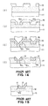
- Figs. 13(a) and 13(b) are diagrams for assistance in explaining a second example of a conventional method of fabricating a semiconductor device, in which a wiring layer is planarised by laser beam irradiation.
- the same reference signs as in Figs. 9 to 12 are applied to the same or corresponding parts.
- an insulating layer 2 is grown on a substrate 1 and an opening portion 2a is formed by etching, as in the case of the first conventional method.
- a wiring layer 4 is grown on the opening portion 2a and on the insulating layer 2 by a normal sputtering method.
- high-output laser beams 8 of extremely short pulse width are then irradiated on the surface of the wiring layer 4. Consequently, the wiring layer 4 is instantaneously melted and viscously flows and is planarised, as shown in Fig. 13(b).
- Figs. 14 show an example of a third conventional method of fabricating a semiconductor device in which a reduced portion of the wiring layer itself, such as is described above, hardly occurs.
- 11 is a semiconductor substrate, 12 an insulating film, 13 a first resist film, 14 a conductive wiring layer, 15 a second resist film, and 16 a third resist film.
- the first resist film 13 is applied and patterned.
- Fig. 14(b) by etching the insulating film 12 with the patterned first resist film 13, grooves 12a and 12b each having a predetermined width are formed.
- the second resist film 15 is applied on the insulating film 12 and patterned. As shown in Fig.
- the insulating film 12 is then etched to form an opening portion 12c underneath the opening portion 12a, and the wiring layer 14 is grown on the insulating film 12 by sputtering so that the grooves 12a, 12b, and the opening portion 12c can be completely covered.
- the third resist film 16 on the wiring layer 14 is patterned as a mask for etching of the wiring layer 14.
- material of the layer is left in place buried in only the grooves 12a, 12b and opening portion 12c, as shown in Fig. 14(d). Since in this method the wiring layer 14 is buried in the grooves 12a, 12b and opening portion 12c, irregularities on the substrate 11 after wiring can be reduced to a very small size.
- a method of fabricating a semiconductor device such as the third conventional example must provide for control of the amount of etching for forming the grooves in the insulating film 12 with high accuracy and make the depths of the groove 12a and the opening portion 12c uniform, because the groove 12a and the window 12c underneath the groove 12a, which are different in width, are formed in the insulating film 12 of a single layer. If the wafer size of the substrate 11 becomes large, the depth of the groove 12a cannot be controlled since the surface area at the time of etching becomes large. When the groove 12a becomes shallow, irregularities on the wiring layer 14 occur on the surface of the insulating layer 12 and the formation of the groove 12a becomes ineffective.
- the wiring layer 14 must be patterned so that the space between the wiring layers 14 becomes narrow, in order to prevent the occurrence of a groove in the form of a crevasse, which is caused by misregistration of patterning. Consequently, a short circuit is liable to arise between adjacent wiring layers 14.
- An embodiment of the present invention can provide a method of fabricating a semiconductor device which is capable of easily and accurately controlling the depth of a groove in which a wiring layer is buried.
- An embodiment of the present invention can provide a method of fabricating a semiconductor device wherein, for a wiring method within the semiconductor device, local burnout of wiring and an increase in resistance are substantially prevented by planarising a metal layer.
- a method of fabricating a semiconductor device according to a first embodiment of the present invention comprises the steps of:-
- the first opening portion is formed in the upper layer insulating film by etching.
- the second opening portion smaller in width than the first opening portion is then formed by etching the lower layer insulating film exposed in the first opening portion.
- the lower layer insulating film serves as an etching stopper as the first opening portion is formed by etching, the first opening portion can be easily and accurately formed to have a predetermined length, and there is no fluctuation in the depth of the first opening portion such as would be caused with the use of the conventional method.
- the metal layer is melted and buried in the first opening portion and second opening portion by laser beam irradiation, the metal layer is uniformly buried in the first opening portion and second opening portion, and a gap within the first opening portion and projection of the metal layer from the first opening portion, as produced with the use of the conventional method, are prevented.
- planarising of the metal layer is completely achieved and thereby can prevent a decrease in operating speeds of circuits after wiring, and can prevent short circuits between adjacent metal layers.
- a method of fabricating a semiconductor device according to a second embodiment of the present invention comprises the steps of:-
- the first insulating film, the second insulating film, and the third insulating film are formed sequentially on the base layer.
- the first opening portion is formed in the third insulating film by etching.
- the second opening portion is formed by etching the second insulating film exposed in the first opening portion and etching the first insulating film.
- the first opening portion can be easily and accurately formed to have a depth proportional to the film thickness of the third insulating film.
- the second opening portion can also be easily formed to have a desired depth by adjusting the film thickness of the first and second insulating films.
- a method of fabricating a semiconductor device according to a third embodiment of the present invention comprises the steps of:-
- the first insulating film and the second insulating film which is smaller in etch rate than the first insulating film and third insulating film, are formed sequentially on the base layer.
- the third insulating film is formed on the second insulating film so that the second insulating film and the first opening portion are covered with the third insulating film.
- the second opening portion which is larger in width than the first opening portion, is formed in the third insulating film on the first opening portion, and also the third opening portion, which is substantially equal in width to the first opening portion, is formed in the first insulating layer.
- the metal layer is buried in the first, second and third opening portions and is planarised by a laser annealing processing.
- the second opening portion can be easily and accurately formed, and at the same time the second opening portion and the third opening portion, which are different in width, are formed, thereby reducing the number of processes.
- the planarising of the metal layer is completely achieved and thereby can prevent a decrease in the operating speeds of circuits after wirings and prevent a short circuit between adjacent metal layers.
- a method of fabricating a semiconductor device according to a fourth embodiment of the present invention comprises the steps of:-
- the first insulating film and the second insulating film which latter film is smaller in etch rate than the first insulating film and the third insulating film, are formed sequentially on the base layer.
- the first opening portion is formed by etching the second and first insulating films, and the third insulating film is formed on the second insulating film so that the second insulating film and the first opening portion are covered with the third insulating film.
- the second opening portion which is larger in width than the first opening portion, is formed in the third insulating film on the first opening portion, and also the side wall insulating film is formed on side walls of the first and second insulating films within the first opening portion.
- the second opening portion can be easily and accurately formed to have a predetermined depth.
- the smaller window for contact is formed within the first opening portion and thereby enhances the operating speed of elements.
- the planarising of the metal layer is completely achieved and thereby can prevent a decrease in the operating speeds of circuits after wirings and prevent a short circuit between adjacent metal layers.
- one of the above-described plurality of insulating films may have absorption rate more than 30% with respect to a laser beam.
- the above-described base layer may comprise aluminium, aluminium base compound, copper, copper base compound, single crystal silicon, polycrystal silicon, or compound semiconductor such as GaAs and AlGaAs.
- the above-described upper or first insulating film may comprise a silicon (Si) oxidation film or a Si oxidation film containing phosphorus (P)
- the second or lower insulating film may comprise Al2O3
- the third insulating film when provided may comprise a silicon (Si) oxidation film or a Si oxidation film containing phosphorus (P).
- the above-described laser beam may comprise an excimer laser beam.
- the metal layer may comprise aluminium (Al), Al base compound, copper (Cu), or Cu base compound.
- 21 is a base layer comprising a conductive material or semiconductor (e.g. aluminium or aluminium base compound, copper or copper base compound, single crystal silicon or polycrystal silicon, or a compound semiconductor such as GaAs and AlGaAs), 22 a lower layer insulating film, 23 an upper layer insulating film, 24 a first opening portion formed in the upper layer insulating film 23, 25 a second opening portion formed in the lower layer insulating film 22, 26 a metal layer, 27 a first resist film, 28 a second resist film, 29 a third resist film, and 30 a laser beam.
- a conductive material or semiconductor e.g. aluminium or aluminium base compound, copper or copper base compound, single crystal silicon or polycrystal silicon, or a compound semiconductor such as GaAs and AlGaAs
- the lower layer insulating film 22 (e.g. alumina (Al2O3)) is deposited on the base layer 21 by sputtering so that it has a predetermined film thickness (e.g. 0.3 ⁇ m).
- the upper layer insulating film 23 (e.g. PSG) larger in etch rate than the lower layer insulating film 22 is then deposited on the lower layer insulating film 22 by a chemical vapour deposition (CVD) method, and the deposited upper layer insulating film 23 has a film thickness of the order of 0.7 ⁇ m.
- a resist film is coated on the upper layer insulating film 23 and the first resist film 27 is formed.
- the first resist film 27 is patterned by a known exposure and development technique so that it is formed with a predetermined opening portion 27a, and the patterned first resist film 27 remains on regions other than a wiring region (opening portion 27a).
- the upper layer insulating film 23 is selectively etched with, for example, CHF4 gas by a RIE (reactive ion etching) method so that the first opening portion 24 corresponding to the opening portion 27a is formed to have a width of the order of 1.8 ⁇ m to 4 ⁇ m and so that the lower layer insulating film 22 is exposed in the first opening portion 24.
- a resist film is then coated to form the second resist film 28 with which the upper layer insulating film 23 and the first opening portion 24 are completely covered.
- the second resist film 28 is patterned by a known exposure and development technique so that an opening portion 28a is formed therein.
- the lower layer insulating film 22 is etched with, for example, argon gas (Ar) so that the second opening portion 25 smaller in width than the first opening portion 24 is formed and serves as a contact window.
- the base layer 21 is exposed to the second opening portion 25 formed in the lower layer insulating film 22.
- Al or Al compound for example, containing Si or Cu
- Al or Al compound is grown to a thickness of the order of 0.6 ⁇ m by sputtering to cover the first opening portion 24, second opening portion 25 and surface of the upper layer insulating film 23. Consequently, the metal layer 26 for wiring is formed and contacts with the base layer 21, as shown in Fig. 1(c).
- a resist film is then coated on the metal layer 26 to form the third resist film 29.
- the third resist film 29 is patterned by a known exposure and development technique so that the resist film 29 becomes slightly larger in width than the first opening portion 24, by about 0.5 ⁇ m at one side.
- the portion of the metal layer 26 which is deposited in locations spaced more than a predetermined dimension (e.g. about 0.5 ⁇ m) from the first opening portion 24 is etched and removed with mixed gases of CCl4 gas and BCl3 gas.
- the remaining metal layer 26 is irradiated by the laser beam 30 of short wavelength and high density (e.g. excimer laser).
- the irradiated metal layer 26 melts and viscously flows, and is buried in the first and second opening portions 24 and 25 and planarised, as shown in Fig. 1(e).
- the laser beams 30 are irradiated with, for example, a pulse width of 50 ns, pulse energy of 150 mJ, pulse irradiation dimension of 2 mm x 2 mm, pulse feed pitch of 0.5 mm, and base layer (21) temperature of 300°C .
- the first opening portion 24 can be easily formed to have a desired depth.
- the metal layer 26 irradiated by the laser beam 30 melts and viscously flows, the first and second opening portions 24 and 25 are filled up with the metal layer 26, and the upper surface 26a of the metal layer 26 becomes substantially flush with an upper surface 23a (Fig. 1(e)) of the upper layer insulating film 23 due to surface tension. Consequently, the metal layer 26 for wiring can be made planar and uniform. This can prevent a decrease in the operating speed of a circuit caused by an increase in a wiring capacity and also prevent a short circuit between metal layers 26 even if they are close to each other.
- the lower layer insulating film 22 comprises Al2O3 and is formed as a relatively thicker film (more than 0.1 ⁇ m), the film 22 has absorption rate more than 30% with respect to the laser beam 30 and therefore can prevent damage to the base layer 21 caused by laser irradiation.
- Figs. 2 and 3 illustrate one example of a method of fabricating a semiconductor device according to a second embodiment of the present invention.
- 41 is a base layer (e.g. a silicon (Si) substrate), 42 a first insulating film (e.g. PSG), 43 a second insulating film (e.g. alumina (Al2O3), 44 a third insulating film (e.g. PSG), 45 a first opening portion formed in the third insulating film 44, 46 an opening portion formed in the third insulating film 44 in close vicinity to the first opening portion 45, 47 a second opening portion formed in the first and second insulating films 42 and 43 and smaller in width than the first opening portion 45, 48 a metal layer for wiring (e.g. Al or Al compound), 49 a first resist film, 50 a second resist film, 51 a third resist film, and 52 a laser beam.
- a metal layer for wiring e.g. Al or Al compound
- a PSG film is grown on the base layer 41 by a chemical vapour deposition (CVD) method, and the first insulating film 42 is formed and has a film thickness of the order of 0.7 ⁇ m.
- Alumina (Al2O3) is then deposited on the first insulating film 42 by sputtering and the second insulating film 43 having a film thickness of the order of 0.15 ⁇ m is formed.
- a PSG film is grown on the second insulating film 43 by the chemical vapour deposition (CVD) method, and the third insulating film 44 is formed.
- a resist film is coated on the third insulating film 44, and the first resist film 49 is formed.
- the first resist film 49 is patterned by a known exposure and development technique so that it is formed with predetermined opening portions 49a and 49b, and the patterned first resist film 49 remains on the regions other than wiring regions (opening portions 49a and 49b).
- the third insulating film 44 is etched by an RIE method so that the first opening portion 45 and opening portion 46 respectively corresponding to the opening portions 49a and 49b are formed.
- the first opening portion 45 has a width of the order of 1.8 ⁇ m to 4 ⁇ m, and the minimum space between the opening portions 45 and 46 is 0.6 ⁇ m.
- the second insulating film 43 is exposed in the opening portions 45 and 46.
- the gas used in the RIE is CHF3
- the gas pressure is 0.05 Torr
- the high-frequency electric power is 13.56 MHz and 4W/cm2.
- the second insulating film 43 comprising Al2O3 is not etched by the RIE and only the third insulating film 44 comprising PSG is etched, selectivity is excellent.
- a resist film is coated to form the second resist film 50 with which the third insulating film 44 and the opening portions 45 and 46 are covered.
- the second resist film 50 is patterned by a known exposure and development technique and formed with an opening portion 50a in which the second insulating film 43 is exposed.
- the second insulating film 43 is etched and formed with an opening portion 47a smaller in width than the first opening portion 45, and the first insulating film 42 is exposed in the opening portion 47a.
- the etching gas is, for example, argon gas (Ar) having a gas pressure of 0.01 Torr, and the etching device with an electric power of 5 W/cm2 is the same as the etching device (not shown) for forming the third insulating film 44.
- Ar argon gas
- the etching device with an electric power of 5 W/cm2 is the same as the etching device (not shown) for forming the third insulating film 44.
- the first insulating film 42 is etched with CHF3 gas and formed with an opening portion 47b which is substantially identical in width with the opening portions 50a and 47a.
- the base layer 41 is exposed in the second opening portion 47 consisting of the opening portions 47a and 47b.
- Al or Al compound is grown to a thickness of the order of 0.6 ⁇ m by sputtering to cover the second opening portion 47, opening portion 46 and third insulating layer 44. Consequently, the metal layer 48 for wiring is formed and contacts with the base layer 41, as shown in Fig. 2(c).
- a resist film is then coated on the metal layer 48 to form the third resist film 51.
- the third resist film 51 is patterned by a known exposure and development technique so that the resist film 51 corresponding to the first opening portion 45 becomes slightly larger in width than the first opening portion 45 and that the resist film 51 corresponding to the opening portion 46 becomes slightly larger in width than the opening portion 46.
- the metal layer 48 is etched with mixed gases (e.g. CCl4 and BCl3 gases) by an RIE method.
- laser beams 52 are irradiated on the metal layer 48 after the third resist film 51 has been removed from the metal layer 48.
- a device for irradiating the laser beams 52 for example, a model 4100 produced by XMR company in the United States may be used, and the laser beam source is an Xe-Cl excimer laser.
- the laser beams 52 are irradiated with a pulse width of 50 ns, pulse energy of 150 mJ, pulse irradiation dimension of 2 mm x 2 mm, pulse feed pitch of 0.5 mm, and base layer (41) temperature of 300°C.
- the metal layer 48 irradiated by the laser beams 52 melts and viscously flows, and is buried in the opening portions 45 and 46 and planarised, as shown in Fig. 2(e).
- the third resist film 51 is patterned so that it becomes larger in width than the opening portions 45 and 46, the metal layer 48 in the first opening portion 45 can be separated from the metal layer 48 in the opening portion 46, as shown in Fig. 2(d), if the space between the opening portions 45 and 46 is more than 1.6 ⁇ m.
- the metal layer 48 in the adjacent opening portions 53, 54, 55 and 56 becomes a continuous pattern, as shown in Fig. 3(a).
- the laser beams 52 are irradiated on the continuous metal layer 48, the melted metal layer 48 flows into the opening portions 53 to 56 and these are separated from one another and the upper surfaces of the separated metal layers 48 are planarised, as shown in Fig. 3(b).
- the second insulating layer 43 is used as an etching stopper and as a light shading film as the first opening portion 45, in which the metal layer 48 for wiring is to be buried, is formed, the first opening portion 45 with a predetermined depth proportional to the film thickness of the third insulating film 44 can be formed with ease and high accuracy.
- the second opening portion 47 can be easily formed to a desired depth by adjusting the film thickness of the first insulating film 42.
- the second insulating film 43 comprises Al2O3 and is formed as a relatively thicker film of more than 0.1 ⁇ m, the film 43 has an absorption rate of more than 30% with respect to the laser beam 52.
- the first insulating film 42 with a relatively larger film thickness is formed underneath the second insulating film 43. Therefore, even if, for example, a p-n junction having a depth of 0.1 ⁇ m is formed on the base layer 41, the p-n junction is normal even after irradiation of the laser beams 52 and no damage occurs in the underlying elements of the region in which the metal layer 48 is not located.
- the base layer 41 comprises a wiring layer containing Al
- a planar upper wiring layer can be formed in the same manner.
- the energy of the laser beam that is irradiated on the base layer 41 containing Al is reduced to below 70% due to the layer containing Al2O3, the Al wiring layer of the base layer 41 does not suffer any damage without melting.
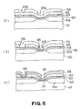
- Figs. 4 and 5 are diagrams used for explaining another example of a method of fabricating a semiconductor device according to the second embodiment of the present invention.
- 61 is a base layer (e.g. a silicon (Si) substrate having thermal oxidation films 61a buried therein), 62 a first insulating film (e.g. PSG), 63 a second insulating film (e.g. alumina (Al2O3)), 64 a third insulating film (e.g. PSG), 65 a first opening portion formed in the third insulating film 64, 66 an opening portion formed in the third insulating film 64 in close vicinity to the first opening portion 65, 67 a second opening portion formed in the first insulating film 62 and smaller in width than the first opening portion 65, 68 a metal layer for wiring (e.g. Al or Al compound), 69 a first resist film, and 70 a second resist film.
- a metal layer for wiring e.g. Al or Al compound
- the thermal oxidation films 61a are formed in the base layer 61 by, for example, a selective oxidation method.
- the thermal oxidation films 61a formed in the base layer 61 each having a film thickness of the order of 0.6 ⁇ m.
- a PSG film is then grown on the base layer 61 and thermal oxidation films 61a by the chemical vapour deposition (CVD) method, and formed into the first insulating film 62 having a film thickness of the order of 0.3 ⁇ m.
- Alumina (Al2O3) is then deposited on the first insulating film 62 by sputtering to form the second insulating film 63 having a film thickness of the order of 0.15 ⁇ m.
- a PSG film is grown on the second insulating film 63 by the chemical vapour deposition (CVD) method, and the third insulating film 64 is formed and has a film thickness of the order of 0.7 ⁇ m.
- a resist film is coated on the third insulating film 64 to form the first resist film 69.
- the first resist film 69 is patterned by a known exposure and development technique so that it is formed with predetermined opening portions 69a and 69b, and the patterned first resist film 69 remains on the regions other than wiring regions (opening portions 69a and 69b).
- the third insulating film 64 is etched by the RIE method so that the first opening portion 65 and the opening portion 66 are formed.
- the second insulating film 63 is exposed in the opening portions 65 and 66.
- a resist film is coated on the third insulating film 64 to form the second resist film 70.
- the second resist film 70 is patterned by a known exposure and development technique so that an opening portion 70a is formed above the first opening portion 65 of the second resist film 70.
- the second insulating film 63 is etched by an RIE method using for example CHF3 gas, and further the first insulating film 62 is etched by the RIE method using for example Ar gas to form the second opening portion 67 in which the base layer 61 is exposed.
- the metal layer 68 is grown to have a thickness of the order of 0.6 ⁇ m by sputtering to cover the second opening portion 67 and third insulating layer 64, and contacts with the base layer 61, as shown in Fig. 5(c).
- the processes thereafter are the same as those of the embodiment described above, and if the processes are complete, a semiconductor device as shown in Fig. 4 will be fabricated.
- the embodiment of Figs. 4 and 5 can also obtain the same effect as the embodiment described above.
- Figs. 6 illustrate an example of a method of fabricating a semiconductor device according to a third embodiment of the present invention.
- 81 is a base layer (e.g. a silicon (Si) substrate), 82 a first insulating film (e.g. PSG), 83 second insulating film (e.g. alumina (Al2O3)), 84 a third insulating film (e.g. PSG), 85 a first opening portion formed in the second insulating film 83, 86 a second opening portion formed in the third insulating film 84, 87 an opening portion formed in the third insulating film 84 in close vicinity to the second opening portion 86, 88 a third opening portion formed in the first insulating film 82, 89 a metal layer for wiring (e.g. Al or Al compound), 90 a second resist film, 91 a third resist film, and 92 a laser beam.
- a metal layer for wiring e.g. Al or Al compound
- a PSG film is grown on the base layer 81 by the chemical vapour deposition (CVD) method, and the first insulating film 82 is formed and has a film thickness of the order of 0.7 ⁇ m.
- Alumina (Al2O3) is then deposited on the first insulating film 82 by sputtering and the second insulating film 83 having a film thickness of the order of 0.15 ⁇ m is formed.
- a resist film is coated on the second insulating film 83 to form a first resist film (not shown), which is patterned by a known exposure and development technique.
- the second insulating film 83 is etched by an RIE method and the first opening portion (or aperture) 85 is formed.
- the gas used in the RIE is for example argon gas, the gas pressure is 0.01 Torr, and the high-frequency electric power is 5W/cm2.
- a PSG film is grown on the second insulating film 83 by the chemical vapour deposition (CVD) method, and the third insulating film 84 is formed and deposited on the second film 83 formed with the first opening portion 85, as shown in Fig. 6(a).
- the third insulating film 84 has a film thickness of the order of 0.7 ⁇ m.
- a resist film is coated on the third insulating film 84 to form the second resist film 90.
- the second resist film 90 is patterned by a known exposure and development technique so that it is formed with predetermined opening portions 90a and 90b.
- the third insulating film 84 and the first insulating film 82 are etched by an RIE method so that the second opening portion 86 larger in width than the first opening portion 85 and also the opening portion 87 are formed in the third insulating film 84 and that the third opening portion 88 substantially equal in width to the first opening portion 85 is formed in the first insulating film 82.
- the base layer 81 is exposed in the third opening portion 88.
- the second opening portion 86 has a width of, for example, 1.8 ⁇ m to 4 ⁇ m, and the minimum space between the second opening portion 86 and the opening portion 87 is 0.6 ⁇ m.
- the gas used in the RIE is for example CHF3 gas, the gas pressure is 0.05 Torr, and the high-frequency electric power is 13.56 MHz and 4W/cm2. Since in this condition Al2O3 is not etched and only PSG is etched, selectivity is excellent. Therefore, the second insulating film 83 becomes an etching stopper with respect to the direction of depth of the second opening portion 86, and the second opening portion 86 and the third opening portion 88 are easily formed at the same time for a short period of time, since the first opening portion 85 contains no Al2O3.
- the metal layer 89 is formed by sputtering so that it covers the third opening portion 88, second opening portion 86, opening portion 87 and third insulating layer 84.
- a resist film is then coated on the metal layer 89 to form the third resist film 91.
- the third resist film 91 is patterned by a known exposure and development technique so that the third resist film 91 corresponding to the second opening portion 86 becomes slightly larger in width than the second opening portion 86 and that the third resist film 91 corresponding to the opening portion 87 becomes slightly larger in width than the opening portion 87.
- the metal layer 89 is etched with mixed gases (e.g. CCl4 and BCl3 gases) by an RIE method.
- the laser beams 92 are irradiated on the metal layers 89.
- the metal layer 89 is buried in the first and third opening portions 85 and 88 and planarised, and also the metal layer 89 is buried in the opening portion 87 and planarised, as shown in Fig. 6(e).
- the second opening portion 86 can be easily formed and the depth of the opening portion 86 accurately adjusted by using the second insulating film 83 as an etching stopper and as a light shading film.
- the second opening portion 86 and the third opening portion 88 which are different in width, are formed at the same time with the same etching gas, so that the number of processes can be reduced.
- the metal layer 89 can be made planar and at the same time a decrease in the operating speed of a circuit and a short circuit between the metal layers 89 can be prevented.
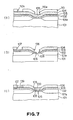
- Figs. 7 illustrate another example of a method of fabricating a semiconductor device according to the third embodiment of the present invention.
- 101 is a base layer (e.g. a silicon (Si) substrate having thermal oxidation films 101a buried therein), 102 a first insulating film (e.g. PSG), 103 a second insulating film (e.g. alumina (Al2O3)), 104 a third insulating film (e.g. PSG), 105 a first opening portion (or aperture) formed in the second insulating film 103, 106 a second opening portion formed in the third insulating film 104, 107 an opening portion formed in the third insulating film 104 in close vicinity to the second opening portion 106, 108 a third opening portion formed in the first insulating layer 102, 109 a metal layer for wiring (e.g. Al or Al compound), and 110 a second resist film.
- a metal layer for wiring e.g. Al or Al compound
- the thermal oxidation films 101a are formed in the base layer 101 by, for example, a selective oxidation method.
- the thermal oxidation films 101a formed in the base layer 101 each have a film thickness of the order of 0.6 ⁇ m.
- a PSG film is then grown on the base layer 101 and thermal oxidation films 101a by the chemical vapour deposition (CVD), and the first insulating film 102 is formed and has a film thickness of the order of 0.3 ⁇ m.
- Alumina (Al2O3) is then deposited on the first insulating film 102 by sputtering and the second insulating film 103 having a film thickness of the order of 0.15 ⁇ m is formed.
- a resist film is coated on the second insulating film 103 to form a first resist film (not shown).
- the second insulating film 103 is etched by an RIE method so that the first opening portion 105 is formed in the film 103.
- a PSG film is grown on the second insulating film 103 formed with the first opening portion 105 by a chemical vapour deposition (CVD) method, so that the third insulating film 104 is formed and has a film thickness of the order of 0.7 ⁇ m.
- a resist film is coated on the third insulating film 104 to form the second resist film 110.
- the first resist film 110 is patterned by a known exposure and development technique so that it is formed with predetermined opening portions 110a and 110b for forming wiring regions.
- the third insulating film 104 is etched by an RIE method so that the second opening portion 106 larger in width than the first opening portion 105 and also the opening portion 107 adjacent to the second opening portion 106 are formed in the third insulating film 104.
- the first insulating film 105 is also etched through the first opening portion 105 to form the third opening portion 108 in which the base layer 101 is exposed.
- Al or Al compound is grown to a thickness of the order of 0.6 ⁇ m on the third insulating film 104 by sputtering to form the metal layer 109 which is contacted through the third opening portion 108 with the base layer 101.
- the laser beams are irradiated as in the above-described embodiments and laser annealing processing is performed. Consequently, the metal layer 109 is buried in the first, second and third opening portions 105, 106 and 108 and planarised, and also the metal layer 109 is buried in the opening portion 107 and planarised.
- the embodiment of Fig. 7 can also obtain the same effect as the embodiment described above.
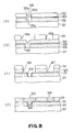
- Fig. 8 illustrates an example of a method of fabricating a semiconductor device according to a fourth embodiment of the present invention.
- 121 is a base layer (e.g. a silicon (Si) substrate), 122 a first insulating film (e.g. PSG), 123 a second insulating film (e.g. alumina (Al2O3)) smaller in etch rate than the first insulating film 122 (PSG), 124 third insulating film (e.g.
- PSG PSG
- 125 a first opening portion formed in the first and second insulating films 122 and 123
- 126 a second opening portion formed in the third insulating film 124
- 127 an opening portion formed in the third insulating film 124 in close vicinity to the second opening portion 126
- 128 a sidewall insulating film formed in the first opening portion 125
- 129 a metal layer for wiring (e.g. Al or Al compound)
- 130 a first resist film
- 131 a second resist film.
- a PSG film is grown on the base layer 121 by a chemical vapour deposition (CVD) method, so that the first insulating film 122 is formed and has a film thickness of the order of 0.7 ⁇ m.
- Alumina (Al2O3) is then deposited on the first insulating film 122 by sputtering and the second insulating film 123 having a film thickness of the order of 0.15 ⁇ m is formed.
- a resist film is coated on the second insulating film 123 to form a first resist film 130, which is patterned by a known exposure and development technique.
- the second insulating film 123 is etched by an RIE method using for example argon (Ar) gas, and an opening portion 125a is formed and the first insulating film 122 is exposed in the opening portion 125a.
- the exposed first insulating film 122 is then etched by an RIE method using for example argon and/or CHF3 gas to form therein an opening portion 125b. That is to say, the first insulating film 122 is exposed to the first opening portion 125 comprising the opening portions 125a and 125b by etching the first insulating film 122 and second insulating film 123.
- a PSG film is grown on the second insulating film 123 by the chemical vapour deposition (CVD) method so that the third insulating film 124 is deposited on the second film 123 and also buries the first opening portion 125.
- a resist film is coated on the third insulating film 124 to form the second resist film 131.
- the second resist film 131 is patterned by a known exposure and development technique so that it is formed with predetermined opening portions 131a and 131b for wiring regions.
- the third insulating film 124 is etched by the RIE method, so that the second opening portion 126 and the opening portion 127 adjacent to the second opening portion 126 are formed.
- the side wall insulating film is formed on the side walls of the first and second insulating films 122 and 123 within the first opening portion 125. In an opening portion defined by the side wall insulating film 128 the base layer 121 is exposed.
- Al or Al compound is grown by sputtering so that it contacts with the base layer 121 exposed in the first opening portion 125, and the metal layer 129 covering the third insulating film 124 is formed.
- the metal layer 129 After formation of the metal layer 129, it is patterned by removing the portions of the metal layer 129, which are spaced a predetermined distance from the second opening portion 126 and from the opening portion 127, by etching. As described above, the laser annealing processing is then performed. Consequently, the metal layer 109 is buried in the first opening portion 125 and second opening portion 126 and planarised.
- the second opening portion 126 can be easily formed and the depth of the opening portion 126 accurately adjusted, because the second insulating film 123 smaller in etch rate than the third insulating film 124 is used as an etching stopper and as a light shading film.
- the side wall insulating film 128 is formed within the first opening portion 125, the exposed area of the base layer 121 can be reduced. Therefore, if a bipolar transistor is formed on the base layer 121, the dimensions of the emitter can be reduced as compared with a normal case having no sidewall insulating film 128. Consequently, an excellent current gain h fe and an excellent switching speed can be obtained.
- copper (Cu) can be grown on the metal layer 48, 68, 89, 109 or 129 so that it has a film thickness of, for example, 300 ⁇ .
- the shape of the wiring layer can be made planar and, furthermore, an electron migration resistance as current flows through wirings can be enhanced, since Cu mixes with Al.
- the reflectivity of Cu with respect to a laser beam is smaller than that of Al, a better energy absorption of the laser beam is obtained.
- the irradiation area of the laser beam is doubled as compared with the case of Al, and the throughput is also enhanced.
- the increase in the irradiation area is also accomplished by a metal layer comprising Cu or Cu compound instead of Al or Al compound.
- the same effect as Cu was also obtained in the case of Ti having a small reflectivity.
- the film thickness of the metal layer after it has been planarised can be made more uniform by making the metal layer in the vicinity of the opening portion, under which an inner window for contact is formed, thicker than the metal layer on other opening portions, or by reducing the width dimension of the opening portion under which an inner window for contact is formed, when the metal layer is etched and patterned.
- the base layers in embodiments of the invention may be Si layers of a semiconductor substrates with diffusion layers, but may also be wiring layers comprising a conductive substance such as a metal. Whilst embodiments of the present invention have been described with a single layer wiring, other embodiments can also be applied to multilayer wiring.
- the insulating film smaller in etch rate that the upper layer as an etching stopper, the depth of the opening portion (groove) of the wiring layer can be controlled easily and accurately, and the wiring layer can be buried within the opening portion and planarised by laser irradiation. As a result, the planarising of the wiring layer can be achieved completely.
- the insulating film having a better absorption with respect to a laser beam, damage to elements by the laser irradiation can be prevented.
- a method of fabricating a semiconductor device embodying the present invention comprises the steps of:-
Landscapes
- Internal Circuitry In Semiconductor Integrated Circuit Devices (AREA)
- Electrodes Of Semiconductors (AREA)
Applications Claiming Priority (2)
| Application Number | Priority Date | Filing Date | Title |
|---|---|---|---|
| JP340971/89 | 1989-12-26 | ||
| JP1340971A JPH03198327A (ja) | 1989-12-26 | 1989-12-26 | 半導体装置の製造方法 |
Publications (2)
| Publication Number | Publication Date |
|---|---|
| EP0435187A2 true EP0435187A2 (de) | 1991-07-03 |
| EP0435187A3 EP0435187A3 (en) | 1993-01-20 |
Family
ID=18342004
Family Applications (1)
| Application Number | Title | Priority Date | Filing Date |
|---|---|---|---|
| EP19900125081 Withdrawn EP0435187A3 (en) | 1989-12-26 | 1990-12-21 | Method of fabricating a semiconductor device |
Country Status (4)
| Country | Link |
|---|---|
| US (1) | US5169800A (de) |
| EP (1) | EP0435187A3 (de) |
| JP (1) | JPH03198327A (de) |
| KR (1) | KR910013542A (de) |
Cited By (13)
| Publication number | Priority date | Publication date | Assignee | Title |
|---|---|---|---|---|
| WO1995019045A1 (de) * | 1994-01-11 | 1995-07-13 | Siemens Aktiengesellschaft | Verfahren zum füllen von kontaktlöchern |
| WO1996012297A3 (en) * | 1994-10-11 | 1996-07-25 | Advanced Micro Devices Inc | Simplified dual damascene process for multilevel metallization and interconnection structure |
| WO1997010612A1 (en) * | 1995-09-14 | 1997-03-20 | Advanced Micro Devices, Inc. | Damascene process for reduced feature size |
| EP0766303A3 (de) * | 1995-09-29 | 1997-04-23 | Toshiba Kk | |
| GB2325083A (en) * | 1997-05-09 | 1998-11-11 | United Microelectronics Corp | A dual damascene process |
| WO2000005763A1 (en) * | 1998-07-23 | 2000-02-03 | Applied Materials, Inc. | Method of producing an interconnect structure for an integrated circuit |
| WO2000022671A1 (en) * | 1998-10-14 | 2000-04-20 | Advanced Micro Devices, Inc. | Method of making dual damascene conductive interconnections and integrated circuit device comprising same |
| WO2000048236A1 (en) * | 1999-02-11 | 2000-08-17 | University Of Bristol | Methods of fabricating etched structures |
| WO2001003179A1 (en) * | 1999-06-30 | 2001-01-11 | Lam Research Corporation | Dual-damascene dielectric structures and methods for making the same |
| DE10200428A1 (de) * | 2002-01-09 | 2003-04-30 | Infineon Technologies Ag | Verfahren zur Herstellung von Kontakten und Leiterbahnen mit Hilfe einer vergrabenen Hartmaske |
| KR100387549B1 (ko) * | 1995-11-28 | 2003-08-19 | 동경 엘렉트론 주식회사 | 피처리기판을가열하면서처리가스를이용해반도체를처리하는방법및그장치 |
| EP0905774A3 (de) * | 1997-09-30 | 2003-11-19 | Infineon Technologies AG | Weiche Passivierungsschicht in der Halbleiterfabrikation |
| CN110571187A (zh) * | 2018-06-05 | 2019-12-13 | 中芯国际集成电路制造(上海)有限公司 | 半导体器件的制造方法 |
Families Citing this family (16)
| Publication number | Priority date | Publication date | Assignee | Title |
|---|---|---|---|---|
| JP2740050B2 (ja) * | 1991-03-19 | 1998-04-15 | 株式会社東芝 | 溝埋込み配線形成方法 |
| JP2907599B2 (ja) * | 1991-08-26 | 1999-06-21 | シャープ株式会社 | 配線層の形成方法 |
| JPH05129296A (ja) * | 1991-11-05 | 1993-05-25 | Fujitsu Ltd | 導電膜の平坦化方法 |
| JPH05160272A (ja) * | 1991-12-04 | 1993-06-25 | Nec Corp | 半導体装置の製造方法 |
| JP3332456B2 (ja) * | 1992-03-24 | 2002-10-07 | 株式会社東芝 | 半導体装置の製造方法及び半導体装置 |
| KR950010041B1 (ko) * | 1992-03-28 | 1995-09-06 | 현대전자산업주식회사 | 콘택 홀(contact hole) 구조 및 그 제조방법 |
| JPH06260441A (ja) * | 1993-03-03 | 1994-09-16 | Nec Corp | 半導体装置の製造方法 |
| US5567329A (en) * | 1995-01-27 | 1996-10-22 | Martin Marietta Corporation | Method and system for fabricating a multilayer laminate for a printed wiring board, and a printed wiring board formed thereby |
| US5587342A (en) * | 1995-04-03 | 1996-12-24 | Motorola, Inc. | Method of forming an electrical interconnect |
| US5942802A (en) | 1995-10-09 | 1999-08-24 | Matsushita Electric Industrial Co., Ltd. | Semiconductor device and method of producing the same |
| JP3402022B2 (ja) * | 1995-11-07 | 2003-04-28 | 三菱電機株式会社 | 半導体装置の製造方法 |
| KR100195329B1 (ko) * | 1996-05-02 | 1999-06-15 | 구본준 | 반도체 소자의 캐패시터 제조 방법 |
| JP2000150516A (ja) | 1998-09-02 | 2000-05-30 | Tokyo Electron Ltd | 半導体装置の製造方法 |
| US6016011A (en) * | 1999-04-27 | 2000-01-18 | Hewlett-Packard Company | Method and apparatus for a dual-inlaid damascene contact to sensor |
| US6635566B1 (en) * | 2000-06-15 | 2003-10-21 | Cypress Semiconductor Corporation | Method of making metallization and contact structures in an integrated circuit |
| JP2011086969A (ja) * | 2011-02-01 | 2011-04-28 | Rohm Co Ltd | 半導体装置およびその製造方法 |
Family Cites Families (9)
| Publication number | Priority date | Publication date | Assignee | Title |
|---|---|---|---|---|
| DE1949174B2 (de) * | 1968-10-02 | 1971-09-23 | Halbleiterbauelement | |
| CA959383A (en) * | 1972-04-05 | 1974-12-17 | North American Rockwell Corporation | Thick oxide process for improving metal deposition and stability of semiconductor devices |
| US4789760A (en) * | 1985-04-30 | 1988-12-06 | Advanced Micro Devices, Inc. | Via in a planarized dielectric and process for producing same |
| US4674176A (en) * | 1985-06-24 | 1987-06-23 | The United States Of America As Represented By The United States Department Of Energy | Planarization of metal films for multilevel interconnects by pulsed laser heating |
| JPS62260319A (ja) * | 1986-05-06 | 1987-11-12 | Mitsubishi Electric Corp | 半導体装置の製造方法 |
| JPS62293740A (ja) * | 1986-06-13 | 1987-12-21 | Fujitsu Ltd | 半導体装置の製造方法 |
| US4920070A (en) * | 1987-02-19 | 1990-04-24 | Fujitsu Limited | Method for forming wirings for a semiconductor device by filling very narrow via holes |
| JPS6466953A (en) * | 1987-09-07 | 1989-03-13 | Nec Corp | Semiconductor device |
| US4758533A (en) * | 1987-09-22 | 1988-07-19 | Xmr Inc. | Laser planarization of nonrefractory metal during integrated circuit fabrication |
-
1989
- 1989-12-26 JP JP1340971A patent/JPH03198327A/ja active Pending
-
1990
- 1990-12-19 US US07/629,795 patent/US5169800A/en not_active Expired - Fee Related
- 1990-12-21 EP EP19900125081 patent/EP0435187A3/en not_active Withdrawn
- 1990-12-26 KR KR1019900021780A patent/KR910013542A/ko not_active Ceased
Cited By (26)
| Publication number | Priority date | Publication date | Assignee | Title |
|---|---|---|---|---|
| WO1995019045A1 (de) * | 1994-01-11 | 1995-07-13 | Siemens Aktiengesellschaft | Verfahren zum füllen von kontaktlöchern |
| US5830803A (en) * | 1994-01-11 | 1998-11-03 | Siemens Aktiengesellschaft | Method for filling contact holes using a doctor blade |
| WO1996012297A3 (en) * | 1994-10-11 | 1996-07-25 | Advanced Micro Devices Inc | Simplified dual damascene process for multilevel metallization and interconnection structure |
| US5635423A (en) * | 1994-10-11 | 1997-06-03 | Advanced Micro Devices, Inc. | Simplified dual damascene process for multi-level metallization and interconnection structure |
| WO1997010612A1 (en) * | 1995-09-14 | 1997-03-20 | Advanced Micro Devices, Inc. | Damascene process for reduced feature size |
| US6077773A (en) * | 1995-09-14 | 2000-06-20 | Advanced Micro Devices, Inc. | Damascene process for reduced feature size |
| US5753967A (en) * | 1995-09-14 | 1998-05-19 | Advanced Micro Devices, Inc. | Damascene process for reduced feature size |
| KR100253852B1 (ko) * | 1995-09-29 | 2000-05-01 | 니시무로 타이죠 | 반도체 장치 및 그 제조 방법 |
| US5976972A (en) * | 1995-09-29 | 1999-11-02 | Kabushiki Kaisha Toshiba | Method of making semiconductor apparatus having wiring groove and contact hole formed in a self-alignment manner |
| EP0766303A3 (de) * | 1995-09-29 | 1997-04-23 | Toshiba Kk | |
| US6163067A (en) * | 1995-09-29 | 2000-12-19 | Kabushiki Kaisha Toshiba | Semiconductor apparatus having wiring groove and contact hole in self-alignment manner |
| KR100387549B1 (ko) * | 1995-11-28 | 2003-08-19 | 동경 엘렉트론 주식회사 | 피처리기판을가열하면서처리가스를이용해반도체를처리하는방법및그장치 |
| GB2325083A (en) * | 1997-05-09 | 1998-11-11 | United Microelectronics Corp | A dual damascene process |
| GB2325083B (en) * | 1997-05-09 | 1999-04-14 | United Microelectronics Corp | A dual damascene process |
| EP0905774A3 (de) * | 1997-09-30 | 2003-11-19 | Infineon Technologies AG | Weiche Passivierungsschicht in der Halbleiterfabrikation |
| US6245662B1 (en) | 1998-07-23 | 2001-06-12 | Applied Materials, Inc. | Method of producing an interconnect structure for an integrated circuit |
| WO2000005763A1 (en) * | 1998-07-23 | 2000-02-03 | Applied Materials, Inc. | Method of producing an interconnect structure for an integrated circuit |
| US6548396B2 (en) | 1998-07-23 | 2003-04-15 | Applied Materials, Inc. | Method of producing an interconnect structure for an integrated circuit |
| US6228758B1 (en) | 1998-10-14 | 2001-05-08 | Advanced Micro Devices, Inc. | Method of making dual damascene conductive interconnections and integrated circuit device comprising same |
| WO2000022671A1 (en) * | 1998-10-14 | 2000-04-20 | Advanced Micro Devices, Inc. | Method of making dual damascene conductive interconnections and integrated circuit device comprising same |
| AU765894B2 (en) * | 1999-02-11 | 2003-10-02 | University Of Bristol, The | Methods of fabricating etched structures |
| WO2000048236A1 (en) * | 1999-02-11 | 2000-08-17 | University Of Bristol | Methods of fabricating etched structures |
| WO2001003179A1 (en) * | 1999-06-30 | 2001-01-11 | Lam Research Corporation | Dual-damascene dielectric structures and methods for making the same |
| DE10200428A1 (de) * | 2002-01-09 | 2003-04-30 | Infineon Technologies Ag | Verfahren zur Herstellung von Kontakten und Leiterbahnen mit Hilfe einer vergrabenen Hartmaske |
| CN110571187A (zh) * | 2018-06-05 | 2019-12-13 | 中芯国际集成电路制造(上海)有限公司 | 半导体器件的制造方法 |
| CN110571187B (zh) * | 2018-06-05 | 2022-03-18 | 中芯国际集成电路制造(上海)有限公司 | 半导体器件的制造方法 |
Also Published As
| Publication number | Publication date |
|---|---|
| EP0435187A3 (en) | 1993-01-20 |
| KR910013542A (ko) | 1991-08-08 |
| US5169800A (en) | 1992-12-08 |
| JPH03198327A (ja) | 1991-08-29 |
Similar Documents
| Publication | Publication Date | Title |
|---|---|---|
| EP0435187A2 (de) | Verfahren zur Herstellung einer Halbleitervorrichtung | |
| EP0063917B1 (de) | Verfahren zur Herstellung eines Halbleiterbauelements | |
| EP0319575B1 (de) | Herstellen von zwischenschicht-leiterbahnen in integrierten schaltungen | |
| EP0162677A2 (de) | Verfahren zur Herstellung einer Halbleitervorrichtung mit einem optischen und einem elektronischen Bauelement | |
| KR0136569B1 (ko) | 고집적 반도체 소자의 콘택홀 형성 방법 | |
| US4584761A (en) | Integrated circuit chip processing techniques and integrated chip produced thereby | |
| CA1045724A (en) | Method for forming integrated circuit regions defined by recessed dielectric isolation | |
| CA1237828A (en) | Semiconductor-on-insulator (soi) device having electrical short to avoid charge accumulation | |
| US4662988A (en) | Semiconductor devices and their fabrication | |
| US3976512A (en) | Method for reducing the defect density of an integrated circuit utilizing ion implantation | |
| US4468414A (en) | Dielectric isolation fabrication for laser trimming | |
| US4497108A (en) | Method for manufacturing semiconductor device by controlling thickness of insulating film at peripheral portion of element formation region | |
| US4980314A (en) | Vapor processing of a substrate | |
| US4729967A (en) | Method of fabricating a junction field effect transistor | |
| US5827756A (en) | Method of manufacturing semiconductor device | |
| US4824800A (en) | Method of fabricating semiconductor devices | |
| US5693548A (en) | Method for making T-gate of field effect transistor | |
| EP0127814B1 (de) | Verfahren zum Herstellen einer schmalen Mesastruktur auf einem Substrat und Verfahren zum Herstellen eines Feldeffekttransistors mit selbstjustiertem Gate | |
| EP0293979A2 (de) | Oxydisolierungsstruktur ohne bird-beak für integrierte Schaltungen | |
| US5225370A (en) | Method of diffusing P type impurity | |
| US5306665A (en) | Manufacturing a wiring for a semiconductor device by a forwardly tapered stack of two conductor films | |
| CA1220561A (en) | Semiconductor device | |
| US4729816A (en) | Isolation formation process with active area protection | |
| EP0978869B1 (de) | Verfahren zur Herstellung eines kleinen Resistmusters sowie Verfahren zur Herstellung einer Gateelektrode | |
| KR0144428B1 (ko) | 반도체 장치의 제조 방법 |
Legal Events
| Date | Code | Title | Description |
|---|---|---|---|
| PUAI | Public reference made under article 153(3) epc to a published international application that has entered the european phase |
Free format text: ORIGINAL CODE: 0009012 |
|
| AK | Designated contracting states |
Kind code of ref document: A2 Designated state(s): DE FR GB |
|
| PUAL | Search report despatched |
Free format text: ORIGINAL CODE: 0009013 |
|
| AK | Designated contracting states |
Kind code of ref document: A3 Designated state(s): DE FR GB |
|
| 17P | Request for examination filed |
Effective date: 19930526 |
|
| 17Q | First examination report despatched |
Effective date: 19940922 |
|
| STAA | Information on the status of an ep patent application or granted ep patent |
Free format text: STATUS: THE APPLICATION IS DEEMED TO BE WITHDRAWN |
|
| 18D | Application deemed to be withdrawn |
Effective date: 19950203 |