EP0435453A2 - Schmalbändiger Hybrid-Halbleiterlaser mit gleichförmiger FM-Antwort - Google Patents
Schmalbändiger Hybrid-Halbleiterlaser mit gleichförmiger FM-Antwort Download PDFInfo
- Publication number
- EP0435453A2 EP0435453A2 EP90312799A EP90312799A EP0435453A2 EP 0435453 A2 EP0435453 A2 EP 0435453A2 EP 90312799 A EP90312799 A EP 90312799A EP 90312799 A EP90312799 A EP 90312799A EP 0435453 A2 EP0435453 A2 EP 0435453A2
- Authority
- EP
- European Patent Office
- Prior art keywords
- response
- laser
- hybrid laser
- hybrid
- section
- Prior art date
- Legal status (The legal status is an assumption and is not a legal conclusion. Google has not performed a legal analysis and makes no representation as to the accuracy of the status listed.)
- Withdrawn
Links
- 230000004044 response Effects 0.000 title abstract description 35
- 239000004065 semiconductor Substances 0.000 title description 8
- 230000003287 optical effect Effects 0.000 claims abstract description 16
- 238000002955 isolation Methods 0.000 claims description 9
- VYPSYNLAJGMNEJ-UHFFFAOYSA-N Silicium dioxide Chemical compound O=[Si]=O VYPSYNLAJGMNEJ-UHFFFAOYSA-N 0.000 claims description 7
- 229910052681 coesite Inorganic materials 0.000 claims description 4
- 229910052906 cristobalite Inorganic materials 0.000 claims description 4
- 239000000377 silicon dioxide Substances 0.000 claims description 4
- 229910052682 stishovite Inorganic materials 0.000 claims description 4
- 229910052905 tridymite Inorganic materials 0.000 claims description 4
- 235000012239 silicon dioxide Nutrition 0.000 claims description 3
- 230000000903 blocking effect Effects 0.000 claims description 2
- 239000003989 dielectric material Substances 0.000 claims 2
- 239000011248 coating agent Substances 0.000 claims 1
- 238000000576 coating method Methods 0.000 claims 1
- 230000008878 coupling Effects 0.000 abstract description 3
- 238000010168 coupling process Methods 0.000 abstract description 3
- 238000005859 coupling reaction Methods 0.000 abstract description 3
- 230000001939 inductive effect Effects 0.000 abstract 1
- 238000002347 injection Methods 0.000 description 12
- 239000007924 injection Substances 0.000 description 12
- 230000007423 decrease Effects 0.000 description 5
- 230000008859 change Effects 0.000 description 3
- 230000001427 coherent effect Effects 0.000 description 3
- 238000004891 communication Methods 0.000 description 3
- 230000035945 sensitivity Effects 0.000 description 3
- 230000008901 benefit Effects 0.000 description 2
- 230000000694 effects Effects 0.000 description 2
- 238000000034 method Methods 0.000 description 2
- 230000008569 process Effects 0.000 description 2
- 229910052581 Si3N4 Inorganic materials 0.000 description 1
- 238000013459 approach Methods 0.000 description 1
- 239000002800 charge carrier Substances 0.000 description 1
- 238000005253 cladding Methods 0.000 description 1
- 238000005259 measurement Methods 0.000 description 1
- 239000013307 optical fiber Substances 0.000 description 1
- 230000005855 radiation Effects 0.000 description 1
- 230000009467 reduction Effects 0.000 description 1
- 229910052710 silicon Inorganic materials 0.000 description 1
- 239000010703 silicon Substances 0.000 description 1
- 230000002269 spontaneous effect Effects 0.000 description 1
Images


Classifications
-
- H—ELECTRICITY
- H01—ELECTRIC ELEMENTS
- H01S—DEVICES USING THE PROCESS OF LIGHT AMPLIFICATION BY STIMULATED EMISSION OF RADIATION [LASER] TO AMPLIFY OR GENERATE LIGHT; DEVICES USING STIMULATED EMISSION OF ELECTROMAGNETIC RADIATION IN WAVE RANGES OTHER THAN OPTICAL
- H01S5/00—Semiconductor lasers
- H01S5/10—Construction or shape of the optical resonator, e.g. extended or external cavity, coupled cavities, bent-guide, varying width, thickness or composition of the active region
- H01S5/14—External cavity lasers
-
- H—ELECTRICITY
- H01—ELECTRIC ELEMENTS
- H01S—DEVICES USING THE PROCESS OF LIGHT AMPLIFICATION BY STIMULATED EMISSION OF RADIATION [LASER] TO AMPLIFY OR GENERATE LIGHT; DEVICES USING STIMULATED EMISSION OF ELECTROMAGNETIC RADIATION IN WAVE RANGES OTHER THAN OPTICAL
- H01S5/00—Semiconductor lasers
- H01S5/0014—Measuring characteristics or properties thereof
-
- H—ELECTRICITY
- H01—ELECTRIC ELEMENTS
- H01S—DEVICES USING THE PROCESS OF LIGHT AMPLIFICATION BY STIMULATED EMISSION OF RADIATION [LASER] TO AMPLIFY OR GENERATE LIGHT; DEVICES USING STIMULATED EMISSION OF ELECTROMAGNETIC RADIATION IN WAVE RANGES OTHER THAN OPTICAL
- H01S5/00—Semiconductor lasers
- H01S5/06—Arrangements for controlling the laser output parameters, e.g. by operating on the active medium
- H01S5/062—Arrangements for controlling the laser output parameters, e.g. by operating on the active medium by varying the potential of the electrodes
- H01S5/0625—Arrangements for controlling the laser output parameters, e.g. by operating on the active medium by varying the potential of the electrodes in multi-section lasers
-
- H—ELECTRICITY
- H01—ELECTRIC ELEMENTS
- H01S—DEVICES USING THE PROCESS OF LIGHT AMPLIFICATION BY STIMULATED EMISSION OF RADIATION [LASER] TO AMPLIFY OR GENERATE LIGHT; DEVICES USING STIMULATED EMISSION OF ELECTROMAGNETIC RADIATION IN WAVE RANGES OTHER THAN OPTICAL
- H01S5/00—Semiconductor lasers
- H01S5/06—Arrangements for controlling the laser output parameters, e.g. by operating on the active medium
- H01S5/0618—Details on the linewidth enhancement parameter alpha
Definitions
- the present invention relates to a semiconductor laser for FM applications and, more particularly, to a hybrid semiconductor laser arrangement with both a narrow linewidth and relatively uniform FM response suitable for coherent communication and sensing applications.
- the Bragg reflector consists of a SiO2 clad Si3N4 core, ridge waveguide of length approximately 3mm, with a first-order diffraction grating imposed on the top-most cladding surface. With this geometry, the Bragg reflector will exhibit a reflection band approximately 6 ⁇ wide.
- the laser and reflector are butt coupled, with alignment of the laser cavity to the waveguide.
- the resultant linewidth measurement for the hybrid device yields a linewidth ( ⁇ ) of less than 200kHz, with a minimum of 110kHz.
- ⁇ linewidth
- a complete description of this device may be found in the article entitled "Compact Silicon-Chip Bragg Reflector Hybrid Laser with 110kHz Linewidth", by D. A. Ackerman et al., appearing in IEEE Eleventh International Conference on Semiconductor Lasers Proceedings, August 1988, at pp. 200-201.
- the uniformity of the FM response is also a concern, which the Ackerman et al. hybrid device does not address.
- the appearance of a phase reversal in the FM response will seriously degrade the performance of the system.
- a phase reversal in the FM response will create an unwanted error signal and thus disrupt system performance.
- Broadband (i.e., a few hundred MHz) and uniform FM response has been obtained utilizing, for example, a multi-electrode laser structure.
- the present invention relates to a semiconductor laser for FM applications and, more particularly, to a hybrid semiconductor laser arrangement with both a relatively narrow linewidth and an essentially uniform FM response.
- a hybrid laser comprises a Fabry-Perot device with two separate gain sections coupled to a narrowband resonant optical reflector.
- the two gain sections of the Fabry-Perot device are biased such that the injection current of one gain section (usually the section coupled to the reflector) is maintained less than the injection current of the other section (which must be biased at least at threshold), so as to create an inhomogeneous linewidth enhancement ( ⁇ ) between the two gain sections.
- ⁇ linewidth enhancement
- the light exiting one facet of the Fabry-Perot device is coupled into the waveguide section of the narrowband resonant optical reflector (ROR) wherein the signal passing into the reflector and re-entering the Fabry-Perot device will have a relatively narrow linewidth.
- the output from the hybrid arrangement is thus the signal exiting the opposite facet (with respect to the ROR) of the Fabry-Perot device.
- FM communication may be achieved by impressing a modulating current, I mod, related to a particular message signal, over the bias current of one of the gain sections.
- I mod a modulating current
- the modulating current I mod is impressed over the lower-valued injection current (usually I b ).
- FIG. 1 illustrates an exemplary hybrid laser arrangement 10 of the present invention.
- hybrid laser 10 comprises a two-electrode Fabry-Perot device 12 including a first gain section 14 and a second gain section 16, with a predetermined amount of electrical isolation R therebetween (typically, greater that 200 ⁇ ).
- device 12 may comprise an InP/InGaAsP buried double heterostructure laser with a stripe geometry (not shown) capable of confining a current to flow in a relatively narrow region.
- the strip geometry is considered well-known in the art and will not be reviewed here.
- isolation R may be achieved by forming a groove 11 between gain sections 14 and 16.
- Isolation may also be achieved by forming an insulating region (e.g., a layer of SiO2) or current blocking region (e.g., a section of Fe-doped InP) between gain sections 14 and 16.
- an insulating region e.g., a layer of SiO2
- current blocking region e.g., a section of Fe-doped InP
- first section 14 of device 12 may also be referred to as the "front section” and second section 16 as the “back section”, where these terms are considered to be interchangeable.
- a separate bias current, I f and I b is applied via electrodes 17 and 19 to front section 14 and back section 16, respectively.
- Back section 16 as seen in FIG. 1, is optically coupled along facet 18 to a narrowband resonant optical reflector (ROR) 20, where in a preferred embodiment facet 18 is AR-coated to prevent multiple transits of the signal within laser 12 and ROR 20.
- ROR narrowband resonant optical reflector
- a modulating current signal I mod is impressed over either I f or I b . In most cases, I mod will be impressed on back section bias current I b .
- the output from arrangement 10 exits facet 22 of first section 14.
- uniform FM response is achieved when the injection currents I b and I f are unequal.
- the inequality in currents results in an inhomogeneous linewidth enhancement factor ( ⁇ ).
- ⁇ linewidth enhancement factor
- the inhomogeniety will provide a relatively uniform FM response.
- the injection current to back section 16, I b may be maintained less than the injection current I f applied to front section 14.
- injection current I f may be maintained less than I b .
- the gain section from which the output signal will exit e.g., front section 14 of FIG. 1 should preferably having the higher injection current value.
- I f >I b the opposite condition (i.e.,I f ⁇ I b ) may be utilized within the scope of the present invention.
- the dependence of the FM response on the injection current is the result of two separate physical processes.
- the first is charge-carrier-induced FM related to the longitudinally inhomogeneous linewidth enhancement factor ( ⁇ ) through the waveguide of each gain section 14,16, created by maintaining I b ⁇ I f (or, alternatively, I f ⁇ I b ).
- the second process is the relatively invariant thermally-induced FM related to the laser being temperature modulated during current modulation.
- the FM response of a non-uniformly biased two-section Fabry-Perot device can be written as: where ⁇ c is defined as the carrier-induced FM response and ⁇ t is defined as the thermally-induced FM response.
- the term may be expressed as where K is a constant relating the frequency shift to the thermal load in the laser junction, ⁇ is the modulating frequency, and ⁇ t is defined as the characteristic frequency (a value of approximately 1 MHz).
- the carrier-induced term ⁇ c has been previously defined in the literature (see O.Nilsson et al., supra , at p.
- n is the total number of photons in the laser
- ⁇ n is the change in the number of photons with intensity modulation
- a f(b) is the rate of stimulated emission/photon for the front(back) section
- B f is the differential rate of stimulated emission with respect to the carrier number
- ⁇ f(b) is the linewidth enhancement factor of the front(back) section
- ⁇ f is the carrier spontaneous lifetime in the front section
- ⁇ is the modulating frequency.
- the first term of equation (3) is related to the effect of having a difference in the linewidth enhancement factor ( ⁇ ) as a result in maintaining different bias currents (I b,f ). If this term is negative (i.e., ⁇ f > ⁇ b ), the laser will exhibit a red-shifted FM response induced by carrier modulation.
- the denominator in the first term gives rise to a rolloff in the FM response at a frequency of (1 + B f ⁇ f )/ ⁇ f , which is typically a few hundred MHz.
- the second term in equation (3) increases in magnitude with increasing frequency, but remains small in comparison to the first term.
- ⁇ c is in phase with ⁇ t and the overall FM response is merely the algebraic sum of equations (2) and (3). Further, if the magnitude of ⁇ c is greater than the magnitude of ⁇ t , the overall FM response will be dominated by ⁇ c .
- the bias current I b applied to back section 16 of hybrid 10 must be maintained at a different value than the bias current I f applied to front section 14. In most cases, I b will be less than I f when maximum output power from front section 14 is desired.
- Linewidth narrowing in hybrid laser 10 is achieved by coupling back section 16 of Fabry-Perot device 12 to a narrowband resonant optical reflector 20.
- a detailed description of an exemplary resonant optical reflector may be found in the article entitled "A Narrow-Band Si3N4-SiO2 Resonant Optical Reflector", by C. H. Henry et al., appearing in the IEEE Journal of Quantum Electronics, Vol. QE-23, No. 9, September 1987, at pp. 1426-8, which is herein incorporated by reference.
- narrowband optical reflector 20 can be defined as an external cavity consisting of an input waveguide disposed next to a high Q resonator in a side-by-side relationship, the resonator comprising a pair of Bragg reflectors which are shifted a quarter wavelength with respect to each other.
- Fabry-Perot device 12 is coupled to ROR 20 at backface 18 such that a resonant reflection results.
- the reflection bandwidth of a typical resonator is known to be less than 0.5 ⁇ .
- FIG. 2 contains a graph illustrating the relationship between the output linewidth ⁇ and bias current I b applied to the modulated section 16 of Fabry-Perot device 12, with a bias current I f on front section 14 fixed at a value of approximately 40mA.
- This decrease in linewidth ⁇ may be attributed to the rate of decrease in the threshold gain as a function of wavelength.
- the slight rise in linewidth at higher bias current levels can be explained by impending mode hop of the laser output as a function of increased biased current.
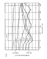
- the FM characteristics change drastically when 1 b is increased beyond 30mA. As shown, at I b 30mA, an FM dip develops at approximately 20MHz, indicating a phase reversal at this frequency. This response indicates that the FM is red-shifted at frequencies below 20MHz and blue-shifted above 20MHz. As 1 b increases further, the FM dip moves to lower frequencies, accompanied by an increase of the blue-shifted FM and further drops in sensitivity.
Landscapes
- Physics & Mathematics (AREA)
- Condensed Matter Physics & Semiconductors (AREA)
- General Physics & Mathematics (AREA)
- Electromagnetism (AREA)
- Optics & Photonics (AREA)
- Semiconductor Lasers (AREA)
- Optical Communication System (AREA)
Applications Claiming Priority (2)
| Application Number | Priority Date | Filing Date | Title |
|---|---|---|---|
| US456991 | 1989-12-26 | ||
| US07/456,991 US5001720A (en) | 1989-12-26 | 1989-12-26 | Hybrid narrow linewidth semiconductor laser with uniform FM response |
Publications (2)
| Publication Number | Publication Date |
|---|---|
| EP0435453A2 true EP0435453A2 (de) | 1991-07-03 |
| EP0435453A3 EP0435453A3 (en) | 1992-01-29 |
Family
ID=23814982
Family Applications (1)
| Application Number | Title | Priority Date | Filing Date |
|---|---|---|---|
| EP19900312799 Withdrawn EP0435453A3 (en) | 1989-12-26 | 1990-11-23 | Hybrid narrow linewidth semiconductor laser with uniform fm response |
Country Status (4)
| Country | Link |
|---|---|
| US (1) | US5001720A (de) |
| EP (1) | EP0435453A3 (de) |
| JP (1) | JP2588489B2 (de) |
| CA (1) | CA2029170C (de) |
Families Citing this family (3)
| Publication number | Priority date | Publication date | Assignee | Title |
|---|---|---|---|---|
| US5077816A (en) * | 1989-12-26 | 1991-12-31 | United Technologies Corporation | Fiber embedded grating frequency standard optical communication devices |
| US5717708A (en) * | 1995-11-09 | 1998-02-10 | Mells; Bradley | Method and apparatus of stabilizing a semiconductor laser |
| US6795472B2 (en) * | 2002-02-05 | 2004-09-21 | Lucent Technologies Inc. | Laser with a resonant optical reflector |
Family Cites Families (10)
| Publication number | Priority date | Publication date | Assignee | Title |
|---|---|---|---|---|
| GB1543405A (en) * | 1975-03-29 | 1979-04-04 | Licentia Gmbh | Method of and arrangement for producing coherent mode radiation |
| US4564946A (en) * | 1983-02-25 | 1986-01-14 | At&T Bell Laboratories | Optical communications system using frequency shift keying |
| JPS60165782A (ja) * | 1984-02-08 | 1985-08-28 | Matsushita Electric Ind Co Ltd | 半導体レ−ザ |
| JPS6155981A (ja) * | 1984-08-27 | 1986-03-20 | Kokusai Denshin Denwa Co Ltd <Kdd> | 半導体発光素子 |
| JPS61164289A (ja) * | 1985-01-16 | 1986-07-24 | Nec Corp | 集積型半導体レ−ザ |
| US4748630A (en) * | 1985-01-17 | 1988-05-31 | Nec Corporation | Optical memory device comprising a semiconductor laser having bistability and two injection current sources for individually controlling the bistability |
| JPS621296A (ja) * | 1985-06-26 | 1987-01-07 | Sharp Corp | 多端子型半導体レ−ザ素子 |
| US4730327A (en) * | 1985-12-16 | 1988-03-08 | Lytel Incorporated | Dual channel fabry-perot laser |
| EP0276071B1 (de) * | 1987-01-21 | 1992-11-11 | AT&T Corp. | Hydridlaser für optisches Nachrichtenwesen |
| JPH01278788A (ja) * | 1988-05-02 | 1989-11-09 | Matsushita Electric Ind Co Ltd | 光帰還型発光装置 |
-
1989
- 1989-12-26 US US07/456,991 patent/US5001720A/en not_active Expired - Lifetime
-
1990
- 1990-11-01 CA CA002029170A patent/CA2029170C/en not_active Expired - Fee Related
- 1990-11-23 EP EP19900312799 patent/EP0435453A3/en not_active Withdrawn
- 1990-12-18 JP JP2411249A patent/JP2588489B2/ja not_active Expired - Fee Related
Also Published As
| Publication number | Publication date |
|---|---|
| CA2029170C (en) | 1995-01-17 |
| US5001720A (en) | 1991-03-19 |
| JPH042192A (ja) | 1992-01-07 |
| JP2588489B2 (ja) | 1997-03-05 |
| EP0435453A3 (en) | 1992-01-29 |
Similar Documents
| Publication | Publication Date | Title |
|---|---|---|
| EP0314490B1 (de) | Halbleiterlaser | |
| US4608697A (en) | Spectral control arrangement for coupled cavity laser | |
| Kobayashi et al. | Single frequency and tunable laser diodes | |
| US5208822A (en) | Semiconductor element having opposite signs of α parameter | |
| EP0300790B1 (de) | Halbleiterlaser | |
| US4677630A (en) | Oscillation frequency stabilized semiconductor laser | |
| Kotaki et al. | Spectral characteristics of a three-section wavelength-tunable DBR laser | |
| US4573163A (en) | Longitudinal mode stabilized laser | |
| US6088373A (en) | Hybrid tunable Bragg laser | |
| Dutta et al. | Electronically tunable distributed feedback lasers | |
| CA1219637A (en) | Laser light sources | |
| US5001720A (en) | Hybrid narrow linewidth semiconductor laser with uniform FM response | |
| US4639922A (en) | Single mode injection laser structure | |
| JP2006504273A (ja) | 波長安定化を行う回折格子を有するポンプレーザのキンクのない動作 | |
| US5119039A (en) | Semiconductor optical amplifier with wideband electrical response | |
| Hong et al. | Enhanced wavelength tuning range in two-section complex-coupled DFB lasers by alternating gain and loss coupling | |
| KR19980024154A (ko) | 광 반도체 장치 및 광원 | |
| KR100429531B1 (ko) | 분포귀환형 반도체 레이저 | |
| US20250309612A1 (en) | Hybrid distributed reflector laser | |
| US20260045767A1 (en) | Distributed reflector laser | |
| JPS63299291A (ja) | 半導体レ−ザ | |
| JP3237499B2 (ja) | 周波数安定化光源 | |
| Hammad et al. | Characterisation of a novel InP photonic integrated circuits for direct modulation applications | |
| Dutta et al. | Tunable Single Wavelength Lasers | |
| Dutta et al. | Single Wavelength Lasers For Coherent Transmission |
Legal Events
| Date | Code | Title | Description |
|---|---|---|---|
| PUAI | Public reference made under article 153(3) epc to a published international application that has entered the european phase |
Free format text: ORIGINAL CODE: 0009012 |
|
| AK | Designated contracting states |
Kind code of ref document: A2 Designated state(s): DE FR GB NL |
|
| PUAL | Search report despatched |
Free format text: ORIGINAL CODE: 0009013 |
|
| AK | Designated contracting states |
Kind code of ref document: A3 Designated state(s): DE FR GB NL |
|
| 17P | Request for examination filed |
Effective date: 19920715 |
|
| 17Q | First examination report despatched |
Effective date: 19930119 |
|
| STAA | Information on the status of an ep patent application or granted ep patent |
Free format text: STATUS: THE APPLICATION IS DEEMED TO BE WITHDRAWN |
|
| 18D | Application deemed to be withdrawn |
Effective date: 19930730 |