EP0435612A2 - Spannungsfolger eingesetzt in Leistungssteuerungsschaltungen - Google Patents
Spannungsfolger eingesetzt in Leistungssteuerungsschaltungen Download PDFInfo
- Publication number
- EP0435612A2 EP0435612A2 EP90314136A EP90314136A EP0435612A2 EP 0435612 A2 EP0435612 A2 EP 0435612A2 EP 90314136 A EP90314136 A EP 90314136A EP 90314136 A EP90314136 A EP 90314136A EP 0435612 A2 EP0435612 A2 EP 0435612A2
- Authority
- EP
- European Patent Office
- Prior art keywords
- voltage
- terminals
- output
- impedance
- control
- Prior art date
- Legal status (The legal status is an assumption and is not a legal conclusion. Google has not performed a legal analysis and makes no representation as to the accuracy of the status listed.)
- Withdrawn
Links
Images
Classifications
-
- H—ELECTRICITY
- H05—ELECTRIC TECHNIQUES NOT OTHERWISE PROVIDED FOR
- H05B—ELECTRIC HEATING; ELECTRIC LIGHT SOURCES NOT OTHERWISE PROVIDED FOR; CIRCUIT ARRANGEMENTS FOR ELECTRIC LIGHT SOURCES, IN GENERAL
- H05B41/00—Circuit arrangements or apparatus for igniting or operating discharge lamps
- H05B41/14—Circuit arrangements
-
- H—ELECTRICITY
- H05—ELECTRIC TECHNIQUES NOT OTHERWISE PROVIDED FOR
- H05B—ELECTRIC HEATING; ELECTRIC LIGHT SOURCES NOT OTHERWISE PROVIDED FOR; CIRCUIT ARRANGEMENTS FOR ELECTRIC LIGHT SOURCES, IN GENERAL
- H05B41/00—Circuit arrangements or apparatus for igniting or operating discharge lamps
- H05B41/14—Circuit arrangements
- H05B41/36—Controlling
-
- H—ELECTRICITY
- H05—ELECTRIC TECHNIQUES NOT OTHERWISE PROVIDED FOR
- H05B—ELECTRIC HEATING; ELECTRIC LIGHT SOURCES NOT OTHERWISE PROVIDED FOR; CIRCUIT ARRANGEMENTS FOR ELECTRIC LIGHT SOURCES, IN GENERAL
- H05B41/00—Circuit arrangements or apparatus for igniting or operating discharge lamps
- H05B41/14—Circuit arrangements
- H05B41/36—Controlling
- H05B41/38—Controlling the intensity of light
- H05B41/39—Controlling the intensity of light continuously
- H05B41/392—Controlling the intensity of light continuously using semiconductor devices, e.g. thyristor
Definitions
- a load power control circuit provides the function of allowing a user to provide this control by adjustment of an element, for example a potentiometer, in the circuit.
- the dimming level is adjusted by varying the value of an external variable control impedance which is connected across a pair of the ballast's control terminals. There is, internal to the ballast, a current source in parallel with a resistance across the pair of ballast control terminals.
- a dimming control signal voltage is created across the control terminals which is sensed by other elements of the ballast's internal circuitry and in response to which vary the illumination level provided by the fixture of which the ballast is a part.
- the control voltage across the control terminals varies from about 1 volt at minimum illumination to about 10 v. at full brightness.
- Each ballast provides power to a pair of fluorescent bulbs.
- control impedance circuit includes active semiconductor elements which make the control characteristics of the impedance circuit as a function of its adjustment potentiometer resistance nearly insensitive to the number of ballasts controlled by the impedance circuit. That is, the illumination level of individual fixtures is very nearly the same for a given mechanical position of the control impedance circuit's adjustable element regardless of the number of ballasts controlled by the impedance.
- the control impedance circuit has the capability of controlling the dimming for as many as 60 individual ballasts.
- the limitation on the number of ballasts which may be controlled by a single control impedance is directly related to the ability of the impedance to sink the current which each individual ballast produces at its control terminals.
- U.S. Patent 4,628,230 shows a light dimming circuit for use with a plurality of lamps and which uses a feedback signal in controlling the illumination level.
- U.S. Patents Nos. 4,645,979; 4,651,060; 4,686,427; 4,704,563; 4,712,045; and 4,717,863 are other references showing dimming circuits for fluorescent lamps.
- the level of power is controlled by adjusting the external impedance across control terminals of a load power control circuit which responds by regulating the power to the load.
- This invention particularly relates to those systems adapted for varying the power supplied to a fluorescent light fixture to vary the illumination from the fixture and which include electronic ballasts which comprise the load power control circuits.
- These load power control circuits provide at their control terminals a voltage which varies in response to the value of a variable control impedance across the control terminals.
- the invention comprises a voltage follower circuit to be interposed between this control impedance and the control terminals of a large number of load power control circuits to recreate at the control terminals of the load power control circuits, the conditions at the output terminals of the control impedance.
- Such a voltage follower circuit has a pair of input terminals to which may be connected the variable control impedance and a pair of output terminals to which may be connected the control terminals of a plurality of said load power control circuits in a ganged configuration so as to allow control a plurality of individual loads with a single variable impedance with substantially unchanged control characteristics.
- the voltage follower circuit in a broadly stated description includes a voltage source; a resistor in series connection with the voltage source across the voltage follower circuit input terminals; a variable impedance having its output terminals forming the output terminals of the voltage follower circuit and an input terminal controlling the impedance between the variable impedance output terminals, and where said impedance increasing as the input terminal voltage decreases and said impedance decreasing as the input terminal voltage increases.
- a voltage sensing means receiving as a first input the voltage across the variable impedance output terminals and as a second input the voltage across the voltage follower circuit input terminals, for providing an output signal to the input terminals of the variable impedance representative of the difference between the voltages of the first and second inputs. This feedback of the voltage across the variable impedance allows the voltage sensing means to drive the variable impedance to accurately mimic the voltage at the input terminals of the voltage follower circuit.
- the particular purpose which this invention achieves is to drive a very large number of loads and achieve simultaneous and identical variation in the power input to them.
- the invention has particular application in controlling with a single control impedance, the power input to large lighting installations having literally hundreds of fixtures.
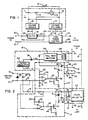
- Fig. 1 is a block diagram of an integrated power and on/off control for a load such as a light fixture.
- Fig. 2 is a circuit diagram for the on/off and power adjusting function of the block diagram of Fig. 1.
- the block diagram shown in Fig. 1 is a block diagram of a circuit providing power adjustment to a load along with an on/off function.
- the user of the load can adjust power and turn it on and off by properly setting a control impedance 10.
- impedance 10 is as a simple variable resistor, in fact its commercial embodiment is instead a circuit including active semiconductor electrical components, the details of which are not relevant to this invention. Power for these active components are received at control terminals 11 and 12 from a DC voltage source 15 in series with a resistor 14.
- the on/off and power level control functions are shown as individual elements in Fig. 1, with the on/off function provided by a voltage sensor 16 and a switch 18.
- switch 18 When switch 18 is closed, electric current passes between switch terminal 24 and switch terminal 25, through load power control circuit 19, and through terminals 22 and 23 to the load.
- the power control function is performed by a voltage follower circuit 17 supplying a control signal through conductor 27 to load power control circuit 19.
- the load power control circuit 19 in the embodiment of this invention pertaining to fluorescent lighting controls comprises the electronic ballast previously discussed.
- Switch 18 under the control of voltage sensor 16 disconnects the load from power terminals 20 and 21 in response to voltage between terminals 11 and 12 falling within a preselected range and connects the load to power terminals 20 and 21 if the voltage between terminals 11 and 12 is outside of this range.
- this preselected voltage range is from .1 to about .5 v.
- voltage sensor 16 provides a signal voltage at terminal 26 to which switch 18 responds by opening the connection between terminals and 24 and 25.
- switch 18 opens electrical connection between terminals 24 and 25. In the range between .5 and .8 v., the condition of switch 18 will not change.
- the voltage produced on terminal 27 of voltage follower circuit 17 in the preferred embodiment precisely emulates or mirrors the voltage between terminals 11 and 12 of impedance 10. It is also preferable that the input interface for these voltage follower circuits 17 be compatible with that of the load power control circuits 19 so that the same commercial embodiment of impedance 10 may be interchangeably connected to the input terminals of either.
- the input interface for load power circuit 19 includes a DC current source and a parallel resistor. The values of resistor 14 and the series voltage source 15 are chosen so that the input interface of voltage follower circuit 17 is compatible with the input of load power control circuit 19.
- the design of voltage follower circuit 17 is such that a substantial number of these voltage follower circuits may be gang connected at their input or control terminals 11 and 12 to impedance 10.
- voltage follower circuit 19 allows the commercially available variable impedance 10 to drive as many as ten voltage followers 17, it can be seen that use of a multiple number of these voltage follower circuits 17 allows as many as 600 individual load power control circuits 19 to be controlled by a single impedance 10 as opposed to the 60 that can be controlled by a single impedance 10 without the interposition of the voltage follower circuit 17.
- Voltage follower 17 and load power control 19 permit one to adjust the power delivered to the load. Again, the impedance between terminals 11 and 12 as measured by sensing the voltage across these terminals control the level of power delivered to the load.
- the design of circuits 17 and 19 is such that the amount of power delivered to the load is highest when the voltage between terminals 11 and 12 is highest and becomes lower as the voltage and impedance across these terminals becomes lower.
- DC voltage source 15 is shown as comprising a transformer 15b receiving power from terminals 20 and 21 and providing a 15 volt AC output to full wave rectifier 15a.
- the output of full wave rectifier 15a is provided to a filter/regulator element 15d through coupling diode 15c.
- the output of filter/regulator element 15d is +12 v. DC provided to the resistor 14 for the control signal and to power the operational amplifiers 35 and 44.
- the unregulated and unfiltered DC output from rectifier 15a is used for certain functions of the switch element 18.
- each operational amplifier 35 and 44 may be taken to be high gain voltage amplifiers having a differential input.
- a differential input is meant that a variable or control voltage can be applied to either or both of the + and - terminals.
- the output of each operational amplifier 35 and 44 is a voltage which is a large multiple, say on the order of several hundred to several thousand, of the difference of the voltage between the plus and minus input terminals.
- the output is simply driven to 0 v. (ground). Because of the large voltage amplification, and the fact that the output voltage can never exceed the voltage of the power applied to these amplifiers, there is a relatively narrow range of input voltage differences over which the output is between the 0 v. and 12 v. extremes.
- the voltage at terminal 12 and provided through resistor 51 is applied to the - input terminal of amplifier 44.
- a feedback voltage is applied to the + input terminal of operational amplifier 44 through resistor 43. The source of this feedback voltage will be identified later.
- the output of amplifier 44 is applied to a voltage divider circuit comprising resistors 45 and 46.
- the output voltage from the voltage divider at the connection between the two resistors 45 and 46 is applied to the base of a transistor 47.
- Transistor 47 functions as a variable impedance to hold the voltage at its collector very close to the voltage on terminal 12.
- the voltage at the collector of transistor 47 forms the feedback voltage mentioned just above provided to the + input terminal of operational amplifier 44.
- a capacitor 52 connected between the + input terminal and the output of operational amplifier 44 provides stability of the amplifier 44 output.
- Current source 55 and resistor 56 provide power for the variable control impedance which for this invention's purpose is connected across the input terminals 11 and 12 instead of being attached to terminal 27 as originally intended.
- Current source 55 and resistor 56 together with power converter 62 comprise the load power control circuit 19 shown in Fig. 1.
- the design of the voltage follower circuit 17 allows complete compatibility between the output of circuit 17 and input of circuit 19.
- a voltage divider comprising resistors 30 and 31 is connected between the output of filter/regulator element 15d and ground.
- the values of resistors 30 and 31 are chosen such that approximately .5 v. appears at the connection between them.
- the voltage produced at the connection between resistors 30 and 31 is applied to the + input terminal of an operational amplifier 35.
- the - terminal input receives the control voltage applied to terminal 12 through resistor 51.
- Resistor 51 is present merely to attenuate potential static discharges presented on terminal 12. Because its resistance may be on the order of 10,000 ohms or so, very much lower than the input impedance of amplifier 35, it has no effect on the response of amplifier 35.
- control input terminals 11 and 12 The voltage across control input terminals 11 and 12 is supplied by the output of filter/regulator element 15d applied through resistor 14.
- filter/regulator element 15d applied through resistor 14.
- the output of amplifier 35 is applied to a pair of series-connected resistors 33 and 34.
- Resistor 33 limits current flow from amplifier 35, and these two resistors also function as a voltage divider to assure that transistor 36 is cut off when the output of amplifier 35 is low.
- a feedback resistor 32 connects the output of amplifier 35 to the + input terminal of amplifier 35. The purpose of resistor 32 is to create a dead band which stabilizes the response of amplifier 35 so that small variations in the - terminal voltage when only slightly more negative (within about .3 v.) than the voltage on the + terminal will not cause the output of amplifier 35 to change.
- the voltage output at the connection between resistors 33 and 34 is applied to the base of an NPN transistor 36.
- the emitter of transistor 36 is connected to ground and the collector is connected to the winding 37 of a first relay.
- the first relay has normally closed contacts 38 controlled by winding 37, so that contacts 38 conduct when transistor 36 is cut off and no current flows through winding 37.
- Unregulated power from full wave rectifier 15a is applied through contacts 38 to a terminal 26 and then to the winding 18a of a second relay comprising the switch 18 discussed in connection with Fig. 1.
- Winding 18a controls normally open contacts 18b which are connected between terminals 24 and 25. It can be seen that when contacts 18b are closed power can flow from terminals 20 and 21 to load terminals 22 and 23 through the power converter element 62 shown.
- Circuit operation is controlled by the value of the impedance connected between terminals 11 and 12.
- the 12 v. potential applied to terminal 12 through resistor 14 is dropped by the control impedance 10 so that voltage varies from a maximum of 10 v. to a minimum of .1 to .2 v.
- voltage at terminal 12 exceeds the .5 v. applied to the + input terminal of amplifier 35
- its output to resistors 33 and 34 is also close to 0 v. so that the voltage at the base of transistor 36 is also 0 v. 0 v. applied to the base of transistor 36 causes transistor 36 to be cut off so that no current flows between its collector and emitter and therefore no current flows through the first relay's winding 37. Therefore, contacts 38 are closed and current flows through the winding 18a which holds contacts 18b closed.
- power can flow to load terminals 22 and 23 through power converter 62.
- resistor 32 shifts the voltage at the + input terminal of amplifier up a few tenths of a volt when the voltage on the - terminal of amplifier is low, and pulls the voltage on the + terminal of amplifier 35 down when the amplifier 35 output is low. Accordingly, resistor 32 adds stability so that normal variations in the voltage across terminals 11 and 12 resulting from fluctuations in power supply voltage or impedance 10 will not trigger amplifier 35 to change its output other than when the voltage at terminal 12 is changed by manual adjustment of impedance 10.
Landscapes
- Control Of Voltage And Current In General (AREA)
- Control Of Electrical Variables (AREA)
- Discharge-Lamp Control Circuits And Pulse- Feed Circuits (AREA)
- Direct Current Feeding And Distribution (AREA)
Applications Claiming Priority (2)
| Application Number | Priority Date | Filing Date | Title |
|---|---|---|---|
| US07/457,214 US5028862A (en) | 1989-12-26 | 1989-12-26 | Voltage follower circuit for use in power level control circuits |
| US457214 | 1989-12-26 |
Publications (2)
| Publication Number | Publication Date |
|---|---|
| EP0435612A2 true EP0435612A2 (de) | 1991-07-03 |
| EP0435612A3 EP0435612A3 (en) | 1992-12-09 |
Family
ID=23815869
Family Applications (1)
| Application Number | Title | Priority Date | Filing Date |
|---|---|---|---|
| EP19900314136 Withdrawn EP0435612A3 (en) | 1989-12-26 | 1990-12-21 | Voltage follower circuit for use in power level control circuits |
Country Status (6)
| Country | Link |
|---|---|
| US (1) | US5028862A (de) |
| EP (1) | EP0435612A3 (de) |
| JP (1) | JPH04313110A (de) |
| KR (1) | KR910014007A (de) |
| AU (1) | AU632390B2 (de) |
| CA (1) | CA2032457A1 (de) |
Families Citing this family (12)
| Publication number | Priority date | Publication date | Assignee | Title |
|---|---|---|---|---|
| US5117178A (en) * | 1991-03-14 | 1992-05-26 | Honeywell Inc. | Fail-safe load power management system |
| US5539261A (en) * | 1993-01-15 | 1996-07-23 | Honeywell Inc. | Mechanical alternate action to electrical pulse converter |
| US5742152A (en) * | 1994-05-12 | 1998-04-21 | Chuntex Eletronic Co., Ltd. | Continuously rectifiable linearity coil circuit |
| JP4159119B2 (ja) * | 1997-08-01 | 2008-10-01 | コーニンクレッカ フィリップス エレクトロニクス エヌ ヴィ | 回路装置及びこの回路装置を具備する信号灯 |
| US7548699B2 (en) * | 2005-12-22 | 2009-06-16 | Avago Technologies Ecbu Ip (Singapore) Pte. Ltd. | Channel-length modulation (CLM) compensation method and apparatus |
| EP2427949B1 (de) | 2009-05-07 | 2020-04-08 | Virginia Electric and Power Company | Spannungserhaltung mit hochentwickelter messinfrastruktur und umspannstationszentralisierte spannungsregelung |
| US9553453B2 (en) | 2013-03-15 | 2017-01-24 | Dominion Resources, Inc. | Management of energy demand and energy efficiency savings from voltage optimization on electric power systems using AMI-based data analysis |
| US9582020B2 (en) | 2013-03-15 | 2017-02-28 | Dominion Resources, Inc. | Maximizing of energy delivery system compatibility with voltage optimization using AMI-based data control and analysis |
| US9847639B2 (en) | 2013-03-15 | 2017-12-19 | Dominion Energy, Inc. | Electric power system control with measurement of energy demand and energy efficiency |
| US9678520B2 (en) | 2013-03-15 | 2017-06-13 | Dominion Resources, Inc. | Electric power system control with planning of energy demand and energy efficiency using AMI-based data analysis |
| US9563218B2 (en) | 2013-03-15 | 2017-02-07 | Dominion Resources, Inc. | Electric power system control with measurement of energy demand and energy efficiency using t-distributions |
| US10732656B2 (en) | 2015-08-24 | 2020-08-04 | Dominion Energy, Inc. | Systems and methods for stabilizer control |
Family Cites Families (7)
| Publication number | Priority date | Publication date | Assignee | Title |
|---|---|---|---|---|
| US4144478A (en) * | 1977-08-11 | 1979-03-13 | Esquire, Inc. | Lamp system take control dimming circuit |
| US4642526A (en) * | 1984-09-14 | 1987-02-10 | Angstrom Robotics & Technologies, Inc. | Fluorescent object recognition system having self-modulated light source |
| US4575654A (en) * | 1984-10-01 | 1986-03-11 | General Electric Company | Piezoceramic coupler control circuit |
| US4628230A (en) * | 1985-08-05 | 1986-12-09 | Mole-Richardson Company | Regulated light dimmer control |
| US4651060A (en) * | 1985-11-13 | 1987-03-17 | Electro Controls Inc. | Method and apparatus for dimming fluorescent lights |
| US4837506A (en) * | 1986-10-02 | 1989-06-06 | Ultraprobe, Inc. | Apparatus including a focused UV light source for non-contact measuremenht and alteration of electrical properties of conductors |
| US4804916A (en) * | 1986-10-28 | 1989-02-14 | Timothy Yablonski | Input voltage compensated, microprocessor controlled, power regulator |
-
1989
- 1989-12-26 US US07/457,214 patent/US5028862A/en not_active Expired - Lifetime
-
1990
- 1990-12-17 CA CA002032457A patent/CA2032457A1/en not_active Abandoned
- 1990-12-18 AU AU68212/90A patent/AU632390B2/en not_active Expired - Fee Related
- 1990-12-21 EP EP19900314136 patent/EP0435612A3/en not_active Withdrawn
- 1990-12-26 KR KR1019900021704A patent/KR910014007A/ko not_active Withdrawn
- 1990-12-26 JP JP2414074A patent/JPH04313110A/ja not_active Withdrawn
Also Published As
| Publication number | Publication date |
|---|---|
| AU632390B2 (en) | 1992-12-24 |
| CA2032457A1 (en) | 1991-06-27 |
| JPH04313110A (ja) | 1992-11-05 |
| KR910014007A (ko) | 1991-08-08 |
| US5028862A (en) | 1991-07-02 |
| EP0435612A3 (en) | 1992-12-09 |
| AU6821290A (en) | 1991-07-04 |
Similar Documents
| Publication | Publication Date | Title |
|---|---|---|
| US5004972A (en) | Integrated power level control and on/off function circuit | |
| US6013988A (en) | Circuit arrangement, and signalling light provided with the circuit arrangement | |
| US5028862A (en) | Voltage follower circuit for use in power level control circuits | |
| US6204613B1 (en) | Protected dimming control interface for an electronic ballast | |
| US4009387A (en) | Automatic energy control lighting system with automatically variable dc source | |
| EP1504316B1 (de) | Pvm-steuerung mit einer automatischen reduktionsschaltung für niedrige batterieleistung und die steuerung enthaltende beleuchtungseinrichtung | |
| EP0435460A2 (de) | Stromverteilungssteuerung für Wechselrichter im Parallelbetrieb | |
| US3524124A (en) | Output voltage limiting circuit for a constant current power supply | |
| EP0487204A2 (de) | Variabler Spannungsregler | |
| US6144539A (en) | Arrangement for protecting low-voltage control circuitry from externally applied high voltages, and dimming ballast employing such an arrangement | |
| US5532894A (en) | Overvoltage protection circuit | |
| US4979067A (en) | Voltage and current limiting power supply | |
| CN1139318A (zh) | 电压平衡电路 | |
| WO1991013530A1 (en) | Apparatus for regulating the intensity of light emitted by a lamp | |
| US5117178A (en) | Fail-safe load power management system | |
| EP0280170A2 (de) | Generator von periodischen Signalen, insbesondere für Schaltnetzteile | |
| US4156150A (en) | Circuit for regulating a DC voltage on which a large AC voltage is superimposed | |
| CN1088291C (zh) | 发射机/接收机装置 | |
| US5552676A (en) | Control device for an appliance consuming electric power | |
| EP0401911B1 (de) | Schaltungsanordnung | |
| EP0240080A1 (de) | Schaltungsanordnung zum Betrieb einer Hochdrucknatriumentladungslampe | |
| JPS6262617A (ja) | 制御回路 | |
| US4518924A (en) | High voltage amplifier | |
| CN119050972B (zh) | 可改变隔离led驱动电源输入/输出侧对地电容分压的电路 | |
| US20050104739A1 (en) | Strobe unit with current limiter |
Legal Events
| Date | Code | Title | Description |
|---|---|---|---|
| PUAI | Public reference made under article 153(3) epc to a published international application that has entered the european phase |
Free format text: ORIGINAL CODE: 0009012 |
|
| AK | Designated contracting states |
Kind code of ref document: A2 Designated state(s): CH DE DK FR GB IT LI NL |
|
| PUAL | Search report despatched |
Free format text: ORIGINAL CODE: 0009013 |
|
| AK | Designated contracting states |
Kind code of ref document: A3 Designated state(s): CH DE DK FR GB IT LI NL |
|
| STAA | Information on the status of an ep patent application or granted ep patent |
Free format text: STATUS: THE APPLICATION IS DEEMED TO BE WITHDRAWN |
|
| 18D | Application deemed to be withdrawn |
Effective date: 19930610 |