EP0436038A1 - Halbleiteranordnung und verfahren zur herstellung - Google Patents
Halbleiteranordnung und verfahren zur herstellung Download PDFInfo
- Publication number
- EP0436038A1 EP0436038A1 EP90910930A EP90910930A EP0436038A1 EP 0436038 A1 EP0436038 A1 EP 0436038A1 EP 90910930 A EP90910930 A EP 90910930A EP 90910930 A EP90910930 A EP 90910930A EP 0436038 A1 EP0436038 A1 EP 0436038A1
- Authority
- EP
- European Patent Office
- Prior art keywords
- insulating film
- semiconductor
- layer
- source
- conductivity type
- Prior art date
- Legal status (The legal status is an assumption and is not a legal conclusion. Google has not performed a legal analysis and makes no representation as to the accuracy of the status listed.)
- Withdrawn
Links
Images



Classifications
-
- H—ELECTRICITY
- H10—SEMICONDUCTOR DEVICES; ELECTRIC SOLID-STATE DEVICES NOT OTHERWISE PROVIDED FOR
- H10D—INORGANIC ELECTRIC SEMICONDUCTOR DEVICES
- H10D30/00—Field-effect transistors [FET]
- H10D30/01—Manufacture or treatment
- H10D30/021—Manufacture or treatment of FETs having insulated gates [IGFET]
- H10D30/027—Manufacture or treatment of FETs having insulated gates [IGFET] of lateral single-gate IGFETs
- H10D30/0278—Manufacture or treatment of FETs having insulated gates [IGFET] of lateral single-gate IGFETs forming single crystalline channels on wafers after forming insulating device isolations
-
- H—ELECTRICITY
- H10—SEMICONDUCTOR DEVICES; ELECTRIC SOLID-STATE DEVICES NOT OTHERWISE PROVIDED FOR
- H10D—INORGANIC ELECTRIC SEMICONDUCTOR DEVICES
- H10D30/00—Field-effect transistors [FET]
- H10D30/60—Insulated-gate field-effect transistors [IGFET]
-
- H—ELECTRICITY
- H10—SEMICONDUCTOR DEVICES; ELECTRIC SOLID-STATE DEVICES NOT OTHERWISE PROVIDED FOR
- H10D—INORGANIC ELECTRIC SEMICONDUCTOR DEVICES
- H10D62/00—Semiconductor bodies, or regions thereof, of devices having potential barriers
- H10D62/10—Shapes, relative sizes or dispositions of the regions of the semiconductor bodies; Shapes of the semiconductor bodies
- H10D62/113—Isolations within a component, i.e. internal isolations
- H10D62/115—Dielectric isolations, e.g. air gaps
- H10D62/116—Dielectric isolations, e.g. air gaps adjoining the input or output regions of field-effect devices, e.g. adjoining source or drain regions
-
- H—ELECTRICITY
- H10—SEMICONDUCTOR DEVICES; ELECTRIC SOLID-STATE DEVICES NOT OTHERWISE PROVIDED FOR
- H10D—INORGANIC ELECTRIC SEMICONDUCTOR DEVICES
- H10D62/00—Semiconductor bodies, or regions thereof, of devices having potential barriers
- H10D62/10—Shapes, relative sizes or dispositions of the regions of the semiconductor bodies; Shapes of the semiconductor bodies
- H10D62/17—Semiconductor regions connected to electrodes not carrying current to be rectified, amplified or switched, e.g. channel regions
- H10D62/213—Channel regions of field-effect devices
- H10D62/221—Channel regions of field-effect devices of FETs
- H10D62/235—Channel regions of field-effect devices of FETs of IGFETs
- H10D62/314—Channel regions of field-effect devices of FETs of IGFETs having vertical doping variations
-
- H—ELECTRICITY
- H10—SEMICONDUCTOR DEVICES; ELECTRIC SOLID-STATE DEVICES NOT OTHERWISE PROVIDED FOR
- H10D—INORGANIC ELECTRIC SEMICONDUCTOR DEVICES
- H10D62/00—Semiconductor bodies, or regions thereof, of devices having potential barriers
- H10D62/10—Shapes, relative sizes or dispositions of the regions of the semiconductor bodies; Shapes of the semiconductor bodies
- H10D62/17—Semiconductor regions connected to electrodes not carrying current to be rectified, amplified or switched, e.g. channel regions
- H10D62/351—Substrate regions of field-effect devices
- H10D62/357—Substrate regions of field-effect devices of FETs
- H10D62/364—Substrate regions of field-effect devices of FETs of IGFETs
- H10D62/371—Inactive supplementary semiconductor regions, e.g. for preventing punch-through, improving capacity effect or leakage current
-
- H—ELECTRICITY
- H10—SEMICONDUCTOR DEVICES; ELECTRIC SOLID-STATE DEVICES NOT OTHERWISE PROVIDED FOR
- H10P—GENERIC PROCESSES OR APPARATUS FOR THE MANUFACTURE OR TREATMENT OF DEVICES COVERED BY CLASS H10
- H10P90/00—Preparation of wafers not covered by a single main group of this subclass, e.g. wafer reinforcement
- H10P90/19—Preparing inhomogeneous wafers
- H10P90/1904—Preparing vertically inhomogeneous wafers
- H10P90/1906—Preparing SOI wafers
- H10P90/1908—Preparing SOI wafers using silicon implanted buried insulating layers, e.g. oxide layers [SIMOX]
-
- H—ELECTRICITY
- H10—SEMICONDUCTOR DEVICES; ELECTRIC SOLID-STATE DEVICES NOT OTHERWISE PROVIDED FOR
- H10W—GENERIC PACKAGES, INTERCONNECTIONS, CONNECTORS OR OTHER CONSTRUCTIONAL DETAILS OF DEVICES COVERED BY CLASS H10
- H10W10/00—Isolation regions in semiconductor bodies between components of integrated devices
- H10W10/10—Isolation regions comprising dielectric materials
- H10W10/181—Semiconductor-on-insulator [SOI] isolation regions, e.g. buried oxide regions of SOI wafers
Definitions
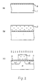
- the process of the prior art for making the metal-oxide semiconductor field effect transistor comprises a step of forming a gate insulating film 4 on a surface portion of a semiconductor substrate 1 as shown in Fig.2 (a), a step of filming a gate electrode material 5 through the gate insulating film 4 as shown in Fig.2 (b), and a step of forming a source 6 and a drain 7 by an ion implantation after having paterned a gate electrode 5 into a predetermined form as shown in Fig.2 (c).
- the drain 7 and the semiconductor substrate 1 has a PN+ junction.
- C D junction capacitance
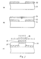
- An object of the present invention is to provide a MISFET which has a small junction capacitance between the substrate and the drain and improved dynamic characteristics.
- the present invention provides the following means.
- the above embodiments show the formation of MISFET using the semiconductor substrates 1, 31, 41 and 61.
- a well may be used instead of a substrate.
Landscapes
- Insulated Gate Type Field-Effect Transistor (AREA)
Applications Claiming Priority (6)
| Application Number | Priority Date | Filing Date | Title |
|---|---|---|---|
| JP183108/89 | 1989-07-14 | ||
| JP183106/89 | 1989-07-14 | ||
| JP18310889A JPH0346371A (ja) | 1989-07-14 | 1989-07-14 | 半導体装置の製造方法 |
| JP1183106A JP2869653B2 (ja) | 1989-07-14 | 1989-07-14 | 半導体装置およびその製造方法 |
| JP18668189A JPH0350743A (ja) | 1989-07-18 | 1989-07-18 | 半導体装置 |
| JP186681/89 | 1989-07-18 |
Publications (2)
| Publication Number | Publication Date |
|---|---|
| EP0436038A1 true EP0436038A1 (de) | 1991-07-10 |
| EP0436038A4 EP0436038A4 (en) | 1991-09-04 |
Family
ID=27325254
Family Applications (1)
| Application Number | Title | Priority Date | Filing Date |
|---|---|---|---|
| EP19900910930 Withdrawn EP0436038A4 (en) | 1989-07-14 | 1990-07-11 | Semiconductor device and method of producing the same |
Country Status (2)
| Country | Link |
|---|---|
| EP (1) | EP0436038A4 (de) |
| WO (1) | WO1991001569A1 (de) |
Cited By (5)
| Publication number | Priority date | Publication date | Assignee | Title |
|---|---|---|---|---|
| FR2673044A1 (fr) * | 1991-02-14 | 1992-08-21 | Mitsubishi Electric Corp | Transistor a effet de champ comprenant une couche enterree, et procede de fabrication. |
| EP0530046A1 (de) * | 1991-08-30 | 1993-03-03 | STMicroelectronics, Inc. | Transistor mit integrierter Schaltung |
| EP0535814A1 (de) * | 1991-09-30 | 1993-04-07 | STMicroelectronics, Inc. | Struktur und Methode für Transistor in integrierter Schaltung |
| US5612230A (en) * | 1991-04-16 | 1997-03-18 | Canon Kabushiki Kaisha | Process for manufacturing a semiconductor device by applying a non-single-crystalline material on a sidewall inside of an opening portion for growing a single-crystalline semiconductor body |
| US6064077A (en) * | 1991-08-30 | 2000-05-16 | Stmicroelectronics, Inc. | Integrated circuit transistor |
Family Cites Families (6)
| Publication number | Priority date | Publication date | Assignee | Title |
|---|---|---|---|---|
| GB1153428A (en) * | 1965-06-18 | 1969-05-29 | Philips Nv | Improvements in Semiconductor Devices. |
| CH455055A (de) * | 1967-03-15 | 1968-04-30 | Ibm | Halbleiteranordnung, bestehend aus einem Substrat, einer Öffnungen enthaltenden Maske und einer durch die Öffnungen mit dem Substrat verbundenen einkristallinen Halbleiterschicht |
| JPS54881A (en) * | 1977-06-03 | 1979-01-06 | Fujitsu Ltd | Semiconductor device |
| JPS56135969A (en) * | 1980-03-27 | 1981-10-23 | Fujitsu Ltd | Manufacture of semiconductor device |
| US4810664A (en) * | 1986-08-14 | 1989-03-07 | Hewlett-Packard Company | Method for making patterned implanted buried oxide transistors and structures |
| JPS63169065A (ja) * | 1987-01-05 | 1988-07-13 | Seiko Instr & Electronics Ltd | 絶縁ゲ−ト電界効果トランジスタ |
-
1990
- 1990-07-11 EP EP19900910930 patent/EP0436038A4/en not_active Withdrawn
- 1990-07-11 WO PCT/JP1990/000889 patent/WO1991001569A1/ja not_active Ceased
Cited By (6)
| Publication number | Priority date | Publication date | Assignee | Title |
|---|---|---|---|---|
| FR2673044A1 (fr) * | 1991-02-14 | 1992-08-21 | Mitsubishi Electric Corp | Transistor a effet de champ comprenant une couche enterree, et procede de fabrication. |
| US5612230A (en) * | 1991-04-16 | 1997-03-18 | Canon Kabushiki Kaisha | Process for manufacturing a semiconductor device by applying a non-single-crystalline material on a sidewall inside of an opening portion for growing a single-crystalline semiconductor body |
| EP0530046A1 (de) * | 1991-08-30 | 1993-03-03 | STMicroelectronics, Inc. | Transistor mit integrierter Schaltung |
| US6064077A (en) * | 1991-08-30 | 2000-05-16 | Stmicroelectronics, Inc. | Integrated circuit transistor |
| US6190179B1 (en) | 1991-08-30 | 2001-02-20 | Stmicroelectronics, Inc. | Method of making a field effect transistor having a channel in an epitaxial silicon layer |
| EP0535814A1 (de) * | 1991-09-30 | 1993-04-07 | STMicroelectronics, Inc. | Struktur und Methode für Transistor in integrierter Schaltung |
Also Published As
| Publication number | Publication date |
|---|---|
| EP0436038A4 (en) | 1991-09-04 |
| WO1991001569A1 (fr) | 1991-02-07 |
Similar Documents
| Publication | Publication Date | Title |
|---|---|---|
| US6767793B2 (en) | Strained fin FETs structure and method | |
| TWI234283B (en) | Novel field effect transistor and method of fabrication | |
| US5087581A (en) | Method of forming vertical FET device with low gate to source overlap capacitance | |
| JP2929291B2 (ja) | 絶縁ゲート電界効果トランジスタの製造方法 | |
| JP3082671B2 (ja) | トランジスタ素子及びその製造方法 | |
| KR100237279B1 (ko) | Misfet, 상보형misfet 및 그 제조방법 | |
| JP3319215B2 (ja) | 絶縁ゲート型半導体装置およびその製造方法 | |
| US5073519A (en) | Method of fabricating a vertical FET device with low gate to drain overlap capacitance | |
| US6331467B1 (en) | Method of manufacturing a trench gate field effect semiconductor device | |
| US11031466B2 (en) | Method of forming oxygen inserted Si-layers in power semiconductor devices | |
| KR930000603B1 (ko) | 반도체장치 및 그 제조방법 | |
| US20070164375A1 (en) | Semiconductor device and manufacturing method thereof | |
| EP0449620B1 (de) | Halbleiteranordnungen mit einer Silizium/Silizium-Germanium-Heterostruktur und Verfahren zu deren Herstellung | |
| US6064077A (en) | Integrated circuit transistor | |
| EP0436038A1 (de) | Halbleiteranordnung und verfahren zur herstellung | |
| US12033851B1 (en) | Left-ISD-LTSEE {low electrostatic field transistor (LEFT) using implanted S/D and selective low temperature epitaxial extension (ISD-LTSEE)} | |
| JP3402548B2 (ja) | 半導体装置の製造方法 | |
| EP0481965B1 (de) | Verfahren zur Herstellung der Statischen Induktionstransistoren mit isoliertem Gatter in einer eingeschnitteten Stufe | |
| JPS6336571A (ja) | 半導体装置 | |
| JPH0350771A (ja) | 半導体装置 | |
| JP2869653B2 (ja) | 半導体装置およびその製造方法 | |
| JPH036863A (ja) | 半導体装置 | |
| JPS63142677A (ja) | 絶縁ゲート電界効果トランジスタの製造方法 | |
| JPH03793B2 (de) | ||
| JP3467288B2 (ja) | バイポーラ動作モードが最適化された垂直接合形電界効果トランジスタ及びその製造方法 |
Legal Events
| Date | Code | Title | Description |
|---|---|---|---|
| PUAI | Public reference made under article 153(3) epc to a published international application that has entered the european phase |
Free format text: ORIGINAL CODE: 0009012 |
|
| 17P | Request for examination filed |
Effective date: 19910312 |
|
| AK | Designated contracting states |
Kind code of ref document: A1 Designated state(s): DE FR GB NL |
|
| A4 | Supplementary search report drawn up and despatched |
Effective date: 19910712 |
|
| AK | Designated contracting states |
Kind code of ref document: A4 Designated state(s): DE FR GB NL |
|
| STAA | Information on the status of an ep patent application or granted ep patent |
Free format text: STATUS: THE APPLICATION IS DEEMED TO BE WITHDRAWN |
|
| 18D | Application deemed to be withdrawn |
Effective date: 19930202 |