EP0436380A2 - Réseau monolithique à diode laser et méthode pour le fabriquer - Google Patents
Réseau monolithique à diode laser et méthode pour le fabriquer Download PDFInfo
- Publication number
- EP0436380A2 EP0436380A2 EP90314245A EP90314245A EP0436380A2 EP 0436380 A2 EP0436380 A2 EP 0436380A2 EP 90314245 A EP90314245 A EP 90314245A EP 90314245 A EP90314245 A EP 90314245A EP 0436380 A2 EP0436380 A2 EP 0436380A2
- Authority
- EP
- European Patent Office
- Prior art keywords
- substrate
- groove
- grooves
- array
- laser diodes
- Prior art date
- Legal status (The legal status is an assumption and is not a legal conclusion. Google has not performed a legal analysis and makes no representation as to the accuracy of the status listed.)
- Granted
Links
Images


Classifications
-
- H—ELECTRICITY
- H01—ELECTRIC ELEMENTS
- H01S—DEVICES USING THE PROCESS OF LIGHT AMPLIFICATION BY STIMULATED EMISSION OF RADIATION [LASER] TO AMPLIFY OR GENERATE LIGHT; DEVICES USING STIMULATED EMISSION OF ELECTROMAGNETIC RADIATION IN WAVE RANGES OTHER THAN OPTICAL
- H01S5/00—Semiconductor lasers
- H01S5/02—Structural details or components not essential to laser action
- H01S5/022—Mountings; Housings
- H01S5/023—Mount members, e.g. sub-mount members
- H01S5/02325—Mechanically integrated components on mount members or optical micro-benches
- H01S5/02326—Arrangements for relative positioning of laser diodes and optical components, e.g. grooves in the mount to fix optical fibres or lenses
-
- H—ELECTRICITY
- H01—ELECTRIC ELEMENTS
- H01S—DEVICES USING THE PROCESS OF LIGHT AMPLIFICATION BY STIMULATED EMISSION OF RADIATION [LASER] TO AMPLIFY OR GENERATE LIGHT; DEVICES USING STIMULATED EMISSION OF ELECTROMAGNETIC RADIATION IN WAVE RANGES OTHER THAN OPTICAL
- H01S5/00—Semiconductor lasers
- H01S5/40—Arrangement of two or more semiconductor lasers, not provided for in groups H01S5/02 - H01S5/30
- H01S5/4018—Lasers electrically in series
-
- H—ELECTRICITY
- H01—ELECTRIC ELEMENTS
- H01S—DEVICES USING THE PROCESS OF LIGHT AMPLIFICATION BY STIMULATED EMISSION OF RADIATION [LASER] TO AMPLIFY OR GENERATE LIGHT; DEVICES USING STIMULATED EMISSION OF ELECTROMAGNETIC RADIATION IN WAVE RANGES OTHER THAN OPTICAL
- H01S5/00—Semiconductor lasers
- H01S5/02—Structural details or components not essential to laser action
- H01S5/022—Mountings; Housings
- H01S5/0235—Method for mounting laser chips
- H01S5/02355—Fixing laser chips on mounts
- H01S5/0237—Fixing laser chips on mounts by soldering
-
- H—ELECTRICITY
- H01—ELECTRIC ELEMENTS
- H01S—DEVICES USING THE PROCESS OF LIGHT AMPLIFICATION BY STIMULATED EMISSION OF RADIATION [LASER] TO AMPLIFY OR GENERATE LIGHT; DEVICES USING STIMULATED EMISSION OF ELECTROMAGNETIC RADIATION IN WAVE RANGES OTHER THAN OPTICAL
- H01S5/00—Semiconductor lasers
- H01S5/02—Structural details or components not essential to laser action
- H01S5/024—Arrangements for thermal management
- H01S5/02407—Active cooling, e.g. the laser temperature is controlled by a thermo-electric cooler or water cooling
- H01S5/02423—Liquid cooling, e.g. a liquid cools a mount of the laser
-
- H—ELECTRICITY
- H01—ELECTRIC ELEMENTS
- H01S—DEVICES USING THE PROCESS OF LIGHT AMPLIFICATION BY STIMULATED EMISSION OF RADIATION [LASER] TO AMPLIFY OR GENERATE LIGHT; DEVICES USING STIMULATED EMISSION OF ELECTROMAGNETIC RADIATION IN WAVE RANGES OTHER THAN OPTICAL
- H01S5/00—Semiconductor lasers
- H01S5/04—Processes or apparatus for excitation, e.g. pumping, e.g. by electron beams
- H01S5/042—Electrical excitation ; Circuits therefor
- H01S5/0428—Electrical excitation ; Circuits therefor for applying pulses to the laser
-
- H—ELECTRICITY
- H01—ELECTRIC ELEMENTS
- H01S—DEVICES USING THE PROCESS OF LIGHT AMPLIFICATION BY STIMULATED EMISSION OF RADIATION [LASER] TO AMPLIFY OR GENERATE LIGHT; DEVICES USING STIMULATED EMISSION OF ELECTROMAGNETIC RADIATION IN WAVE RANGES OTHER THAN OPTICAL
- H01S5/00—Semiconductor lasers
- H01S5/40—Arrangement of two or more semiconductor lasers, not provided for in groups H01S5/02 - H01S5/30
- H01S5/4025—Array arrangements, e.g. constituted by discrete laser diodes or laser bar
- H01S5/4031—Edge-emitting structures
Definitions
- the present invention relates to a one-dimensional or two-dimensional laser diode array, and particularly to a structure for mounting one or a plurality of laser diodes on a monolithic substrate as a subassembly of a working laser device, and to a method of fabrication of such a subassembly.
- the invention has application in many areas in which high power semiconductor laser arrays are used, including satellite communications, directed energy applications, remote sensing of atmospheric conditions, range finding, and isotope separation. Other applications include optical recording, computing, laser machining, level sensing, and remote sensing.
- the inventive monolithic laser diode array includes a monolithic substrate having at least one groove formed therein; a metallization layer provided along the side walls of that groove; and at least one laser diode that fits into the groove.
- the monolithic substrate may be flexible, bending so as to open up the metallized grooves sufficiently to allow insertion of the laser diode into the device, the diodes being secured through force provided by the walls of the metallized grooves.
- the metallized grooves may be slightly larger than the laser diode to be inserted therein, adhesive or other bonding material being used to secure the laser diode within the metallized groove.
- a method of fabricating monolithic laser diode arrays comprising the following steps: providing a monolithic substrate; forming one or more grooves in the substrate; depositing a metallization layer along side walls of the grooves; and disposing a plurality of laser diodes in the metallized grooves.
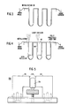
- a monolithic substrate 10 which may be formed of BeO (which may be small grain BeO), AlN, or any highly thermally conductive material, preferably ceramic is, in this embodiment, approximately 0.500 ⁇ x 0.400 ⁇ x 0.025 ⁇ .
- a substrate that is 2.00 ⁇ x 2.00 ⁇ x 0.025 ⁇ (generally an industry standard for ceramics) may be used.
- the thickness of the substrate also may vary; for example, a 40 mil thick substrate also is an industry standard.
- the first formed substrate may be relatively large, and then may be cut into smaller arrays, or submounts, at an appropriate step in the fabrication process.
- the substrate 10 may be polished on both sides to a 3 to 4 ⁇ m finish, and the overall thickness is reduced to 25 mils.
- a groove 20 is formed approximately 0.018 ⁇ deep and 0.004 ⁇ wide, along the second of the above-mentioned dimensions.
- the groove 20 may be wider at the top than at the bottom, depending on manufacturing conditions.
- the groove 20 may be provided with a rounded bottom as shown.
- the grooves 20 shown in Fig. 2 preferably have substantially the same dimensions. In Fig. 2, a 0.004 ⁇ separation between adjacent grooves is provided, and a 0.050 ⁇ margin is provided on either side. Thus, for a substrate 0.500 ⁇ wide, 50 grooves may be cut. However, it should be understood that the design is not limited to these dimensions.
- the grooves may be farther apart or closer together, as required by the end user of the array.
- metallization layer 30 is provided, using one or more of Cr, Ti, Ni, Au, or Ag, or alloys thereof, or any suitably conductive material that adheres sufficiently to the substrate, with a standard metal evaporator or any other suitable plating technique, such as that used in the fabrication of printed circuit boards.
- Cr or Ti may be used first, because they bond well to the substrate material (which usually is ceramic).
- a thick layer of Ni may be applied, to handle the current that will flow through the metallization layer.
- a layer of Au may be provided, because it may be used to form thermocompression bonds.
- the metallized grooves may be perhaps a few tenths of a mil smaller than the overall thickness of the laser diodes to be inserted therein. According to another preferred embodiment, the grooves may be slightly larger than the laser diodes.
- Metallization may be removed from the bottom of each groove by shadowing or masking, which are well-known industry standard metallization techniques, in order to provide electrical isolation.
- the metallized substrates are sized and isolated to form arrays of a suitable size. For example, a 2.00 ⁇ x 2.00 ⁇ array may be cut into individual 1 cm2 arrays.
- laser diodes 40 then may be loaded into each array, as shown in Fig. 4. This may be done in one of at least two presently preferred ways, depending on whether the metallized grooves are narrower than the diodes to be inserted therein. If the metallized grooves are narrower, then the array is loaded into a device capable of performing controlled bending, or flexure, of the substrate 10, by providing a force from the bottom of the substrate toward the top. This flexure enables temporary enlargement, or widening of each groove, to facilitate insertion of the laser diodes 40.
- the assembly 200 includes two L-shaped pieces 210 with respective grooves 220 formed therein, into which the substrate 10 fits.
- the pieces 210 are retractable away from each other to permit insertion of the substrate, whereupon the pieces may be urged toward each other to hold the substrate.
- a flexure member 230 having a curved upper surface is provided between the L-shaped members. To achieve flexure of the substrate, the flexure member 230 is urged upwardly toward a bottom of the substrate 10. It should be noted that uniformity of depth of the grooves 20 is important to the achievement of proper flexure; nonuniform grooves can lead to fracture of the substrate at the point of the shallowest groove.
- the bending of the substrate is terminated, establishing good mechanical and electrical contact between the laser diodes 40 and their respective metallized grooves.
- the electrical contact is sufficient at least to allow pre-testing of the diodes at low power, so that faulty diodes can be replaced before effecting permanent attachment (if such is either necessary or desired), as for example by thermocompression bonding.
- One aspect of the "bending" approach is that it may be possible to rely on compressive forces of the substrate material to secure the laser diodes permanently in the substrate, without having to resort to additional process steps. Such an approach can reduce the number of parts required for assembly. Nevertheless, whether the metallized grooves are wider or narrower than the laser diodes, adhesion of the diodes in the grooves may be effected as follows.
- the pretested laser array may be placed in a vacuum oven, and (assuming gold is used for the metallization layer), the array is heated to allow the gold metallization to enter the plastic stage, thus removing stresses induced during prior assembly stages, and forming a gold thermocompression bond between the laser diode 40 and the substrate 10.
- Other attachment approaches also are possible, and would include standard reflow, or the use of adhesives, such as a conductive Ag, Au, Cu, or Al filled epoxy, or any epoxy containing particulate which will provide thermal and electrical continuity.
- the laser diodes 40 may be facet coated with a multi-layer high reflectance dielectric stack if it is desired to achieve single ended emission, so that light is emitted only from the top of the array.
- Fig. 4 shows laser diodes placed in a submount.
- such submounts can be easier to work with than a larger mount.
- insertion of laser diodes into a smaller structure is easier.
- using smaller submounts, in a modular approach makes it easier to form arrays of different configurations. Also, customers often request such small submounts.
- any commercially manufactured laser diode may be used in the inventive array.
- One such laser diode is manufactured by NorthEast Semiconductor, Inc. (NSI) as quantum well heterostructure laser diode bars, formed using molecular beam epitaxy (MBE) techniques.
- NBI NorthEast Semiconductor, Inc.
- MBE molecular beam epitaxy
- This approach has been found to be preferable to organometallic vapor phase epitaxy with respect to both uniformity over a 3 ⁇ diameter deposition area, and with respect to toxic sources used. Uniformity is particularly important in reducing fabrication costs, to avoid the need for wavelength sorting of processed laser bars which generally must fall within a narrow spectral window.
- NSI has achieved less than 1 nm variation in emission wavelength over a 2 ⁇ GaAs substrate, and less than 3 nm run to run variation.
- GRINSH-SQW graded index separate confining heterostructure single quantum well
- Fig. 6A shows a 2D array module with a eutectic bond 70, which may be gold, and a BeO heat spreader (which is optional) and electrical interconnect 75 with electrical isolation points 80. Heat flows from the array, through the heat spreader; light goes in the opposite direction. Instead of a heat spreader, a thicker substrate 10 may be used, in which case the thicker bottom portion of the substrate would spread heat.
- Fig. 6B shows the Fig. 6A structure, bonded via a solder bond 90 to a water-cooled copper heat sink 100.
- a polymide, fiberglass, or other suitable insulator 110 also is provided.
- Fig. 7 shows a plurality of the arrays of Fig. 5, formed into a larger overall array that measures 2.00 ⁇ x 2.00 ⁇ x 1.00 ⁇ .
- At a 2.5% duty cycle there is 100kW peak power dissipation.
- the power requirements are 500A x 400V, for 200kW input peak.
- 40 gallons per hour flow rate is provided through the water-cooled copper heat sink.
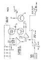
- Fig. 8 shows one implementation of driving circuitry for the Fig. 7 array. Any other appropriate driving circuitry may be used, so long as the above-mentioned power requirements are met.
- metallization and/or isolation within the substrate may be accomplished through patterning and/or mechanical isolation (i. e. cutting into the substrate).
- metallization and/or isolation within the substrate may be accomplished through patterning and/or mechanical isolation (i. e. cutting into the substrate).
Landscapes
- Physics & Mathematics (AREA)
- Condensed Matter Physics & Semiconductors (AREA)
- General Physics & Mathematics (AREA)
- Electromagnetism (AREA)
- Optics & Photonics (AREA)
- Semiconductor Lasers (AREA)
Applications Claiming Priority (2)
| Application Number | Priority Date | Filing Date | Title |
|---|---|---|---|
| US07/460,459 US5040187A (en) | 1990-01-03 | 1990-01-03 | Monolithic laser diode array |
| US460459 | 1990-01-03 |
Publications (3)
| Publication Number | Publication Date |
|---|---|
| EP0436380A2 true EP0436380A2 (fr) | 1991-07-10 |
| EP0436380A3 EP0436380A3 (en) | 1992-02-26 |
| EP0436380B1 EP0436380B1 (fr) | 1995-04-26 |
Family
ID=23828796
Family Applications (1)
| Application Number | Title | Priority Date | Filing Date |
|---|---|---|---|
| EP90314245A Expired - Lifetime EP0436380B1 (fr) | 1990-01-03 | 1990-12-24 | Réseau monolithique à diode laser et méthode pour le fabriquer |
Country Status (4)
| Country | Link |
|---|---|
| US (1) | US5040187A (fr) |
| EP (1) | EP0436380B1 (fr) |
| JP (1) | JP2858964B2 (fr) |
| DE (1) | DE69018956T2 (fr) |
Cited By (6)
| Publication number | Priority date | Publication date | Assignee | Title |
|---|---|---|---|---|
| EP0556639A1 (fr) * | 1992-02-03 | 1993-08-25 | Sumitomo Electric Industries, Limited | Dispositif laser à semi-conducteur |
| FR2720872A1 (fr) * | 1994-06-07 | 1995-12-08 | Thomson Csf Semiconducteurs | Pile de barrettes de diodes laser, et son procédé d'assemblage. |
| EP0687047A1 (fr) * | 1994-06-07 | 1995-12-13 | Thomson-Csf Semiconducteurs Specifiques | Pile de barrettes de diodes laser, et son procédé d'assemblage |
| US5542018A (en) * | 1990-08-31 | 1996-07-30 | Kuhara; Yoshiki | Semiconductor laser device making use of photodiode chip |
| US5778020A (en) * | 1996-06-04 | 1998-07-07 | Cj Laser, Inc. | ND: YAG laser pump head |
| EP1511135A1 (fr) * | 2003-08-27 | 2005-03-02 | Northrop Grumman Corporation | Réseau monolithique de diodes lasers refroidi par immersion et sa méthode de fabrication |
Families Citing this family (62)
| Publication number | Priority date | Publication date | Assignee | Title |
|---|---|---|---|---|
| US5128951A (en) * | 1991-03-04 | 1992-07-07 | Karpinski Arthur A | Laser diode array and method of fabrication thereof |
| US5305344A (en) * | 1993-04-29 | 1994-04-19 | Opto Power Corporation | Laser diode array |
| US5394427A (en) * | 1994-04-29 | 1995-02-28 | Cutting Edge Optronics, Inc. | Housing for a slab laser pumped by a close-coupled light source |
| US5572541A (en) * | 1994-10-13 | 1996-11-05 | Coherent Technologies, Inc. | Laser rod assembly for side pumped lasers |
| US5659413A (en) | 1995-02-28 | 1997-08-19 | The Mitre Corporation | Laser satellite communication system |
| US5610930A (en) * | 1995-03-02 | 1997-03-11 | Hughes Aircraft Company | Voltage adding diode laser array |
| US6188707B1 (en) * | 1995-03-20 | 2001-02-13 | Timothy L. Irwin | Mounting structure for laser diode bars |
| US5627850A (en) * | 1995-03-20 | 1997-05-06 | Paradigm Lasers, Inc. | Laser diode array |
| US5548605A (en) * | 1995-05-15 | 1996-08-20 | The Regents Of The University Of California | Monolithic microchannel heatsink |
| US5825803A (en) * | 1995-12-14 | 1998-10-20 | Institut National D'optique | Multiple emitter laser diode assembly with graded-index fiber microlens |
| US5898211A (en) * | 1996-04-30 | 1999-04-27 | Cutting Edge Optronics, Inc. | Laser diode package with heat sink |
| US5734672A (en) * | 1996-08-06 | 1998-03-31 | Cutting Edge Optronics, Inc. | Smart laser diode array assembly and operating method using same |
| US5909458A (en) * | 1996-11-27 | 1999-06-01 | The Regents Of The University Of California | Low-cost laser diode array |
| US5835518A (en) * | 1997-01-31 | 1998-11-10 | Star Medical Technologies, Inc. | Laser diode array packaging |
| US5828683A (en) * | 1997-04-21 | 1998-10-27 | The Regents Of The University Of California | High density, optically corrected, micro-channel cooled, v-groove monolithic laser diode array |
| US6151341A (en) * | 1997-05-30 | 2000-11-21 | Excel/Quantronix, Inc. | Stackable integrated diode packaging |
| US6219369B1 (en) | 1997-06-09 | 2001-04-17 | Laserfare Advanced Technology Group | Phased matched surface emitting diode laser |
| US6240116B1 (en) | 1997-08-14 | 2001-05-29 | Sdl, Inc. | Laser diode array assemblies with optimized brightness conservation |
| US6295307B1 (en) | 1997-10-14 | 2001-09-25 | Decade Products, Inc. | Laser diode assembly |
| US5995289A (en) | 1997-12-15 | 1999-11-30 | The University Of Utah Research Foundation | Laser beam coupler, shaper and collimator |
| US6259713B1 (en) | 1997-12-15 | 2001-07-10 | The University Of Utah Research Foundation | Laser beam coupler, shaper and collimator device |
| US6195376B1 (en) * | 1998-03-31 | 2001-02-27 | Opto Power Corporation | Semiconductor laser array stack package & method of fabrication |
| US5913108A (en) * | 1998-04-30 | 1999-06-15 | Cutting Edge Optronics, Inc. | Laser diode packaging |
| US6400740B1 (en) | 1998-10-22 | 2002-06-04 | Laser Diode Array, Inc. | Laser diode apparatus with support structure |
| US6636538B1 (en) | 1999-03-29 | 2003-10-21 | Cutting Edge Optronics, Inc. | Laser diode packaging |
| US6330259B1 (en) | 1999-06-24 | 2001-12-11 | Jonathan S. Dahm | Monolithic radial diode-pumped laser with integral micro channel cooling |
| US6266353B1 (en) * | 1999-07-30 | 2001-07-24 | The Regents Of The University Of California | Monolithic laser diode array with one metalized sidewall |
| CA2284946A1 (fr) | 1999-10-04 | 2001-04-04 | Institut National D'optique | Ensemble de reseaux de diodes laser fait d'un substrat monolithique nervure |
| US6647035B1 (en) | 2000-10-17 | 2003-11-11 | The Regents Of The University Of California | Ruggedized microchannel-cooled laser diode array with self-aligned microlens |
| US6782161B2 (en) | 2001-02-05 | 2004-08-24 | Derma Laser Inc. | Laser diode apparatus provided with an aiming beam and injection method therefor |
| US20020110165A1 (en) * | 2001-02-14 | 2002-08-15 | Filgas David M. | Method and system for cooling at least one laser diode with a cooling fluid |
| US6700913B2 (en) | 2001-05-29 | 2004-03-02 | Northrop Grumman Corporation | Low cost high integrity diode laser array |
| EP1278278A1 (fr) | 2001-07-18 | 2003-01-22 | Nanyang Technological University | Laser à l'état solide pompé par diodes |
| US6757309B1 (en) | 2001-11-07 | 2004-06-29 | Laser Diode Array, Inc. | Low inductance laser diode arrays, laser diode array assemblies, and fabrication thereof |
| US6927086B2 (en) * | 2002-09-24 | 2005-08-09 | Decade Products, Inc. | Method and apparatus for laser diode assembly and array |
| US7170919B2 (en) | 2003-06-23 | 2007-01-30 | Northrop Grumman Corporation | Diode-pumped solid-state laser gain module |
| US7495848B2 (en) * | 2003-07-24 | 2009-02-24 | Northrop Grumman Corporation | Cast laser optical bench |
| US7305016B2 (en) * | 2005-03-10 | 2007-12-04 | Northrop Grumman Corporation | Laser diode package with an internal fluid cooling channel |
| US7656915B2 (en) * | 2006-07-26 | 2010-02-02 | Northrop Grumman Space & Missions Systems Corp. | Microchannel cooler for high efficiency laser diode heat extraction |
| US7864825B2 (en) | 2006-08-10 | 2011-01-04 | Lasertel, Inc. | Method and system for a laser diode bar array assembly |
| US20080056314A1 (en) * | 2006-08-31 | 2008-03-06 | Northrop Grumman Corporation | High-power laser-diode package system |
| US20080089371A1 (en) * | 2006-10-11 | 2008-04-17 | Patrick Reichert | Bright light source with two-dimensional array of diode-laser emitters |
| US8236036B1 (en) | 2007-07-21 | 2012-08-07 | Frost Ricky A | Optical dermatological and medical treatment apparatus having replaceable laser diodes |
| US7724791B2 (en) * | 2008-01-18 | 2010-05-25 | Northrop Grumman Systems Corporation | Method of manufacturing laser diode packages and arrays |
| WO2010017619A1 (fr) * | 2008-08-13 | 2010-02-18 | Institut National D'optique | Dispositif d'éclairage à diodes laser, et procédé de conditionnement optique du faisceau lumineux émis par ce dispositif |
| US8160115B2 (en) * | 2009-01-21 | 2012-04-17 | Coherent, Inc. | Two-dimensional diode-laser array with broad-band output |
| US8345720B2 (en) * | 2009-07-28 | 2013-01-01 | Northrop Grumman Systems Corp. | Laser diode ceramic cooler having circuitry for control and feedback of laser diode performance |
| US8660156B2 (en) * | 2009-09-03 | 2014-02-25 | Lawrence Livermore National Security, Llc | Method and system for powering and cooling semiconductor lasers |
| JP5313180B2 (ja) * | 2010-01-19 | 2013-10-09 | シャープ株式会社 | レーザー定着装置 |
| US9590388B2 (en) | 2011-01-11 | 2017-03-07 | Northrop Grumman Systems Corp. | Microchannel cooler for a single laser diode emitter based system |
| WO2012100124A1 (fr) * | 2011-01-20 | 2012-07-26 | Dilas Diode Laser, Inc. | Ensemble laser combiné dans l'espace et procédé de combinaison de faisceaux laser |
| US8937976B2 (en) | 2012-08-15 | 2015-01-20 | Northrop Grumman Systems Corp. | Tunable system for generating an optical pulse based on a double-pass semiconductor optical amplifier |
| US20170117683A1 (en) | 2015-10-22 | 2017-04-27 | Northrup Grumman Space and Mission Systems Corp. | Thermally conductive, current carrying, electrically isolated submount for laser diode arrays |
| US11025031B2 (en) | 2016-11-29 | 2021-06-01 | Leonardo Electronics Us Inc. | Dual junction fiber-coupled laser diode and related methods |
| US10589508B2 (en) | 2016-12-15 | 2020-03-17 | General Electric Company | Additive manufacturing systems and methods |
| US11406004B2 (en) | 2018-08-13 | 2022-08-02 | Leonardo Electronics Us Inc. | Use of metal-core printed circuit board (PCB) for generation of ultra-narrow, high-current pulse driver |
| US11056854B2 (en) | 2018-08-14 | 2021-07-06 | Leonardo Electronics Us Inc. | Laser assembly and related methods |
| US11296481B2 (en) | 2019-01-09 | 2022-04-05 | Leonardo Electronics Us Inc. | Divergence reshaping array |
| US11752571B1 (en) | 2019-06-07 | 2023-09-12 | Leonardo Electronics Us Inc. | Coherent beam coupler |
| US12253685B2 (en) | 2019-09-16 | 2025-03-18 | Leonardo Electronics Us Inc. | Asymmetric input intensity hexagonal homogenizer |
| US20220360039A1 (en) * | 2019-09-30 | 2022-11-10 | Osram Opto Semiconductors Gmbh | Laser package and system with laser packages |
| CN114883909A (zh) * | 2022-05-24 | 2022-08-09 | 无锡亮源激光技术有限公司 | 一种准连续半导体激光器列阵叠层结构及制作方法 |
Family Cites Families (6)
| Publication number | Priority date | Publication date | Assignee | Title |
|---|---|---|---|---|
| US3622906A (en) * | 1967-10-24 | 1971-11-23 | Rca Corp | Light-emitting diode array |
| JPS5414181A (en) * | 1977-07-04 | 1979-02-02 | Fujitsu Ltd | Semiconductor laser unit |
| JPS6042888A (ja) * | 1983-08-18 | 1985-03-07 | Toshiba Corp | 半導体レ−ザ素子の端面保護膜形成方法 |
| JPH071794B2 (ja) * | 1985-07-23 | 1995-01-11 | 松下電器産業株式会社 | ハイブリッド光ic装置およびその製造方法 |
| JPS62128586A (ja) * | 1985-11-29 | 1987-06-10 | Matsushita Electric Ind Co Ltd | 光電子集積回路の製造方法 |
| US4881237A (en) * | 1988-08-26 | 1989-11-14 | Massachusetts Institute Of Technology | Hybrid two-dimensional surface-emitting laser arrays |
-
1990
- 1990-01-03 US US07/460,459 patent/US5040187A/en not_active Expired - Lifetime
- 1990-12-24 DE DE69018956T patent/DE69018956T2/de not_active Expired - Fee Related
- 1990-12-24 EP EP90314245A patent/EP0436380B1/fr not_active Expired - Lifetime
- 1990-12-28 JP JP2415676A patent/JP2858964B2/ja not_active Expired - Fee Related
Cited By (9)
| Publication number | Priority date | Publication date | Assignee | Title |
|---|---|---|---|---|
| US5542018A (en) * | 1990-08-31 | 1996-07-30 | Kuhara; Yoshiki | Semiconductor laser device making use of photodiode chip |
| EP0556639A1 (fr) * | 1992-02-03 | 1993-08-25 | Sumitomo Electric Industries, Limited | Dispositif laser à semi-conducteur |
| FR2720872A1 (fr) * | 1994-06-07 | 1995-12-08 | Thomson Csf Semiconducteurs | Pile de barrettes de diodes laser, et son procédé d'assemblage. |
| EP0687047A1 (fr) * | 1994-06-07 | 1995-12-13 | Thomson-Csf Semiconducteurs Specifiques | Pile de barrettes de diodes laser, et son procédé d'assemblage |
| US5778020A (en) * | 1996-06-04 | 1998-07-07 | Cj Laser, Inc. | ND: YAG laser pump head |
| US6101208A (en) * | 1996-06-04 | 2000-08-08 | Diode Pumped Laser Technologies, Inc. | Nd:YAG laser pump head |
| EP1511135A1 (fr) * | 2003-08-27 | 2005-03-02 | Northrop Grumman Corporation | Réseau monolithique de diodes lasers refroidi par immersion et sa méthode de fabrication |
| JP2005072549A (ja) * | 2003-08-27 | 2005-03-17 | Northrop Grumman Corp | 液浸冷却のレーザ・ダイオード装置 |
| US7016383B2 (en) | 2003-08-27 | 2006-03-21 | Northrop Grumman Corporation | Immersion-cooled monolithic laser diode array and method of manufacturing the same |
Also Published As
| Publication number | Publication date |
|---|---|
| JPH0629623A (ja) | 1994-02-04 |
| DE69018956T2 (de) | 1995-12-21 |
| US5040187A (en) | 1991-08-13 |
| EP0436380A3 (en) | 1992-02-26 |
| EP0436380B1 (fr) | 1995-04-26 |
| DE69018956D1 (de) | 1995-06-01 |
| JP2858964B2 (ja) | 1999-02-17 |
Similar Documents
| Publication | Publication Date | Title |
|---|---|---|
| US5040187A (en) | Monolithic laser diode array | |
| US5284790A (en) | Method of fabricating monolithic laser diode array | |
| US5128951A (en) | Laser diode array and method of fabrication thereof | |
| JP3386963B2 (ja) | レーザダイオードデバイスの製造方法 | |
| JP5513707B2 (ja) | 半導体発光デバイスの相互接続 | |
| EP1887666B1 (fr) | Procédé pour l'assemblage de réseaux de barres de diodes laser | |
| US5311530A (en) | Semiconductor laser array | |
| EP2786459B1 (fr) | Procédé pour fabriquer des piles de diodes laser à haute densité | |
| US20070170453A1 (en) | Package for mounting an optical element and a method of manufacturing the same | |
| JPH11340581A (ja) | レ―ザダイオ―ドパッケ―ジング | |
| WO1992019027A1 (fr) | Ensemble plane mince destine a refroidir un alignement de diodes laser a emission le long d'un bord | |
| WO1998034271A9 (fr) | Boitier pour groupes de diodes lasers | |
| WO1998034271A1 (fr) | Boitier pour groupes de diodes lasers | |
| KR20010013085A (ko) | 발광 소자의 제조 방법 | |
| WO2016133943A1 (fr) | Configurations de diodes laser densément espacées | |
| KR101217590B1 (ko) | 히트 싱크 상에서 측면으로 광학적으로 펌핑된 표면발광반도체 레이저 | |
| NL1007390C2 (nl) | Hoogvermogen diodenlaser en werkwijze voor het monteren daarvan. | |
| JP4904150B2 (ja) | 発光素子の製造方法 | |
| US5959352A (en) | Chip arrangement and method of producing the same | |
| JP4543651B2 (ja) | ヒートシンク並びにヒートシンクを備えた光源装置 | |
| JP4778627B2 (ja) | レーザダイオード用サブマウント及びその製造方法 | |
| CN114204407B (zh) | 激光器管芯的封装结构及封装方法 | |
| KR0121688Y1 (ko) | 반도체 레이저장치 | |
| CA2293925C (fr) | Ensemble de diodes laser |
Legal Events
| Date | Code | Title | Description |
|---|---|---|---|
| PUAI | Public reference made under article 153(3) epc to a published international application that has entered the european phase |
Free format text: ORIGINAL CODE: 0009012 |
|
| AK | Designated contracting states |
Kind code of ref document: A2 Designated state(s): DE FR GB |
|
| PUAL | Search report despatched |
Free format text: ORIGINAL CODE: 0009013 |
|
| AK | Designated contracting states |
Kind code of ref document: A3 Designated state(s): DE FR GB |
|
| 17P | Request for examination filed |
Effective date: 19920806 |
|
| 17Q | First examination report despatched |
Effective date: 19930323 |
|
| GRAA | (expected) grant |
Free format text: ORIGINAL CODE: 0009210 |
|
| AK | Designated contracting states |
Kind code of ref document: B1 Designated state(s): DE FR GB |
|
| REF | Corresponds to: |
Ref document number: 69018956 Country of ref document: DE Date of ref document: 19950601 |
|
| ET | Fr: translation filed | ||
| PLBE | No opposition filed within time limit |
Free format text: ORIGINAL CODE: 0009261 |
|
| STAA | Information on the status of an ep patent application or granted ep patent |
Free format text: STATUS: NO OPPOSITION FILED WITHIN TIME LIMIT |
|
| 26N | No opposition filed | ||
| REG | Reference to a national code |
Ref country code: GB Ref legal event code: IF02 |
|
| PGFP | Annual fee paid to national office [announced via postgrant information from national office to epo] |
Ref country code: FR Payment date: 20061220 Year of fee payment: 17 |
|
| PGFP | Annual fee paid to national office [announced via postgrant information from national office to epo] |
Ref country code: GB Payment date: 20061222 Year of fee payment: 17 |
|
| PGFP | Annual fee paid to national office [announced via postgrant information from national office to epo] |
Ref country code: DE Payment date: 20070131 Year of fee payment: 17 |
|
| GBPC | Gb: european patent ceased through non-payment of renewal fee |
Effective date: 20071224 |
|
| PG25 | Lapsed in a contracting state [announced via postgrant information from national office to epo] |
Ref country code: DE Free format text: LAPSE BECAUSE OF NON-PAYMENT OF DUE FEES Effective date: 20080701 |
|
| REG | Reference to a national code |
Ref country code: FR Ref legal event code: ST Effective date: 20081020 |
|
| PG25 | Lapsed in a contracting state [announced via postgrant information from national office to epo] |
Ref country code: GB Free format text: LAPSE BECAUSE OF NON-PAYMENT OF DUE FEES Effective date: 20071224 |
|
| PG25 | Lapsed in a contracting state [announced via postgrant information from national office to epo] |
Ref country code: FR Free format text: LAPSE BECAUSE OF NON-PAYMENT OF DUE FEES Effective date: 20071231 |