EP0437355B1 - Procédé et appareillage pour fabriquer un dispositif électroluminescent à film mince - Google Patents
Procédé et appareillage pour fabriquer un dispositif électroluminescent à film mince Download PDFInfo
- Publication number
- EP0437355B1 EP0437355B1 EP91300159A EP91300159A EP0437355B1 EP 0437355 B1 EP0437355 B1 EP 0437355B1 EP 91300159 A EP91300159 A EP 91300159A EP 91300159 A EP91300159 A EP 91300159A EP 0437355 B1 EP0437355 B1 EP 0437355B1
- Authority
- EP
- European Patent Office
- Prior art keywords
- gas
- source material
- material gas
- zone
- area
- Prior art date
- Legal status (The legal status is an assumption and is not a legal conclusion. Google has not performed a legal analysis and makes no representation as to the accuracy of the status listed.)
- Expired - Lifetime
Links
- 238000000034 method Methods 0.000 title claims description 25
- 239000010409 thin film Substances 0.000 title claims description 11
- 239000007789 gas Substances 0.000 claims description 67
- 239000000463 material Substances 0.000 claims description 46
- 239000000758 substrate Substances 0.000 claims description 33
- 238000006243 chemical reaction Methods 0.000 claims description 21
- 238000009792 diffusion process Methods 0.000 claims description 10
- 230000008021 deposition Effects 0.000 claims description 8
- 229910021380 Manganese Chloride Inorganic materials 0.000 claims description 7
- GLFNIEUTAYBVOC-UHFFFAOYSA-L Manganese chloride Chemical compound Cl[Mn]Cl GLFNIEUTAYBVOC-UHFFFAOYSA-L 0.000 claims description 7
- 239000011565 manganese chloride Substances 0.000 claims description 7
- 125000006850 spacer group Chemical group 0.000 claims description 5
- 239000012159 carrier gas Substances 0.000 claims description 3
- 238000011144 upstream manufacturing Methods 0.000 claims description 3
- 239000005132 Calcium sulfide based phosphorescent agent Substances 0.000 claims description 2
- 239000011592 zinc chloride Substances 0.000 claims description 2
- JIAARYAFYJHUJI-UHFFFAOYSA-L zinc dichloride Chemical compound [Cl-].[Cl-].[Zn+2] JIAARYAFYJHUJI-UHFFFAOYSA-L 0.000 claims description 2
- 230000001419 dependent effect Effects 0.000 claims 1
- 239000010408 film Substances 0.000 description 45
- 229910052984 zinc sulfide Inorganic materials 0.000 description 25
- 238000005229 chemical vapour deposition Methods 0.000 description 14
- 238000009826 distribution Methods 0.000 description 8
- 238000010438 heat treatment Methods 0.000 description 7
- 238000000151 deposition Methods 0.000 description 6
- 238000012216 screening Methods 0.000 description 6
- 230000000694 effects Effects 0.000 description 5
- 238000000313 electron-beam-induced deposition Methods 0.000 description 5
- 229910052581 Si3N4 Inorganic materials 0.000 description 3
- 238000004519 manufacturing process Methods 0.000 description 3
- VYPSYNLAJGMNEJ-UHFFFAOYSA-N Silicium dioxide Chemical compound O=[Si]=O VYPSYNLAJGMNEJ-UHFFFAOYSA-N 0.000 description 2
- 239000011521 glass Substances 0.000 description 2
- 238000004020 luminiscence type Methods 0.000 description 2
- 230000000704 physical effect Effects 0.000 description 2
- 229920006395 saturated elastomer Polymers 0.000 description 2
- 235000012431 wafers Nutrition 0.000 description 2
- BLRPTPMANUNPDV-UHFFFAOYSA-N Silane Chemical compound [SiH4] BLRPTPMANUNPDV-UHFFFAOYSA-N 0.000 description 1
- 230000002411 adverse Effects 0.000 description 1
- PNEYBMLMFCGWSK-UHFFFAOYSA-N aluminium oxide Inorganic materials [O-2].[O-2].[O-2].[Al+3].[Al+3] PNEYBMLMFCGWSK-UHFFFAOYSA-N 0.000 description 1
- 229910052681 coesite Inorganic materials 0.000 description 1
- 229910052593 corundum Inorganic materials 0.000 description 1
- 229910052906 cristobalite Inorganic materials 0.000 description 1
- 238000005566 electron beam evaporation Methods 0.000 description 1
- 238000005530 etching Methods 0.000 description 1
- 238000011156 evaluation Methods 0.000 description 1
- 238000009413 insulation Methods 0.000 description 1
- 239000004973 liquid crystal related substance Substances 0.000 description 1
- 238000005259 measurement Methods 0.000 description 1
- 239000002184 metal Substances 0.000 description 1
- 229910052751 metal Inorganic materials 0.000 description 1
- 239000000843 powder Substances 0.000 description 1
- 239000004065 semiconductor Substances 0.000 description 1
- 239000000377 silicon dioxide Substances 0.000 description 1
- 229910052682 stishovite Inorganic materials 0.000 description 1
- WGPCGCOKHWGKJJ-UHFFFAOYSA-N sulfanylidenezinc Chemical group [Zn]=S WGPCGCOKHWGKJJ-UHFFFAOYSA-N 0.000 description 1
- 238000012360 testing method Methods 0.000 description 1
- 229910052905 tridymite Inorganic materials 0.000 description 1
- 229910001845 yogo sapphire Inorganic materials 0.000 description 1
Images




Classifications
-
- C—CHEMISTRY; METALLURGY
- C23—COATING METALLIC MATERIAL; COATING MATERIAL WITH METALLIC MATERIAL; CHEMICAL SURFACE TREATMENT; DIFFUSION TREATMENT OF METALLIC MATERIAL; COATING BY VACUUM EVAPORATION, BY SPUTTERING, BY ION IMPLANTATION OR BY CHEMICAL VAPOUR DEPOSITION, IN GENERAL; INHIBITING CORROSION OF METALLIC MATERIAL OR INCRUSTATION IN GENERAL
- C23C—COATING METALLIC MATERIAL; COATING MATERIAL WITH METALLIC MATERIAL; SURFACE TREATMENT OF METALLIC MATERIAL BY DIFFUSION INTO THE SURFACE, BY CHEMICAL CONVERSION OR SUBSTITUTION; COATING BY VACUUM EVAPORATION, BY SPUTTERING, BY ION IMPLANTATION OR BY CHEMICAL VAPOUR DEPOSITION, IN GENERAL
- C23C16/00—Chemical coating by decomposition of gaseous compounds, without leaving reaction products of surface material in the coating, i.e. chemical vapour deposition [CVD] processes
- C23C16/44—Chemical coating by decomposition of gaseous compounds, without leaving reaction products of surface material in the coating, i.e. chemical vapour deposition [CVD] processes characterised by the method of coating
- C23C16/455—Chemical coating by decomposition of gaseous compounds, without leaving reaction products of surface material in the coating, i.e. chemical vapour deposition [CVD] processes characterised by the method of coating characterised by the method used for introducing gases into reaction chamber or for modifying gas flows in reaction chamber
- C23C16/45502—Flow conditions in reaction chamber
-
- C—CHEMISTRY; METALLURGY
- C23—COATING METALLIC MATERIAL; COATING MATERIAL WITH METALLIC MATERIAL; CHEMICAL SURFACE TREATMENT; DIFFUSION TREATMENT OF METALLIC MATERIAL; COATING BY VACUUM EVAPORATION, BY SPUTTERING, BY ION IMPLANTATION OR BY CHEMICAL VAPOUR DEPOSITION, IN GENERAL; INHIBITING CORROSION OF METALLIC MATERIAL OR INCRUSTATION IN GENERAL
- C23C—COATING METALLIC MATERIAL; COATING MATERIAL WITH METALLIC MATERIAL; SURFACE TREATMENT OF METALLIC MATERIAL BY DIFFUSION INTO THE SURFACE, BY CHEMICAL CONVERSION OR SUBSTITUTION; COATING BY VACUUM EVAPORATION, BY SPUTTERING, BY ION IMPLANTATION OR BY CHEMICAL VAPOUR DEPOSITION, IN GENERAL
- C23C16/00—Chemical coating by decomposition of gaseous compounds, without leaving reaction products of surface material in the coating, i.e. chemical vapour deposition [CVD] processes
- C23C16/22—Chemical coating by decomposition of gaseous compounds, without leaving reaction products of surface material in the coating, i.e. chemical vapour deposition [CVD] processes characterised by the deposition of inorganic material, other than metallic material
- C23C16/30—Deposition of compounds, mixtures or solid solutions, e.g. borides, carbides, nitrides
- C23C16/305—Sulfides, selenides, or tellurides
- C23C16/306—AII BVI compounds, where A is Zn, Cd or Hg and B is S, Se or Te
-
- C—CHEMISTRY; METALLURGY
- C23—COATING METALLIC MATERIAL; COATING MATERIAL WITH METALLIC MATERIAL; CHEMICAL SURFACE TREATMENT; DIFFUSION TREATMENT OF METALLIC MATERIAL; COATING BY VACUUM EVAPORATION, BY SPUTTERING, BY ION IMPLANTATION OR BY CHEMICAL VAPOUR DEPOSITION, IN GENERAL; INHIBITING CORROSION OF METALLIC MATERIAL OR INCRUSTATION IN GENERAL
- C23C—COATING METALLIC MATERIAL; COATING MATERIAL WITH METALLIC MATERIAL; SURFACE TREATMENT OF METALLIC MATERIAL BY DIFFUSION INTO THE SURFACE, BY CHEMICAL CONVERSION OR SUBSTITUTION; COATING BY VACUUM EVAPORATION, BY SPUTTERING, BY ION IMPLANTATION OR BY CHEMICAL VAPOUR DEPOSITION, IN GENERAL
- C23C16/00—Chemical coating by decomposition of gaseous compounds, without leaving reaction products of surface material in the coating, i.e. chemical vapour deposition [CVD] processes
- C23C16/44—Chemical coating by decomposition of gaseous compounds, without leaving reaction products of surface material in the coating, i.e. chemical vapour deposition [CVD] processes characterised by the method of coating
- C23C16/455—Chemical coating by decomposition of gaseous compounds, without leaving reaction products of surface material in the coating, i.e. chemical vapour deposition [CVD] processes characterised by the method of coating characterised by the method used for introducing gases into reaction chamber or for modifying gas flows in reaction chamber
- C23C16/45512—Premixing before introduction in the reaction chamber
-
- C—CHEMISTRY; METALLURGY
- C23—COATING METALLIC MATERIAL; COATING MATERIAL WITH METALLIC MATERIAL; CHEMICAL SURFACE TREATMENT; DIFFUSION TREATMENT OF METALLIC MATERIAL; COATING BY VACUUM EVAPORATION, BY SPUTTERING, BY ION IMPLANTATION OR BY CHEMICAL VAPOUR DEPOSITION, IN GENERAL; INHIBITING CORROSION OF METALLIC MATERIAL OR INCRUSTATION IN GENERAL
- C23C—COATING METALLIC MATERIAL; COATING MATERIAL WITH METALLIC MATERIAL; SURFACE TREATMENT OF METALLIC MATERIAL BY DIFFUSION INTO THE SURFACE, BY CHEMICAL CONVERSION OR SUBSTITUTION; COATING BY VACUUM EVAPORATION, BY SPUTTERING, BY ION IMPLANTATION OR BY CHEMICAL VAPOUR DEPOSITION, IN GENERAL
- C23C16/00—Chemical coating by decomposition of gaseous compounds, without leaving reaction products of surface material in the coating, i.e. chemical vapour deposition [CVD] processes
- C23C16/44—Chemical coating by decomposition of gaseous compounds, without leaving reaction products of surface material in the coating, i.e. chemical vapour deposition [CVD] processes characterised by the method of coating
- C23C16/455—Chemical coating by decomposition of gaseous compounds, without leaving reaction products of surface material in the coating, i.e. chemical vapour deposition [CVD] processes characterised by the method of coating characterised by the method used for introducing gases into reaction chamber or for modifying gas flows in reaction chamber
- C23C16/45559—Diffusion of reactive gas to substrate
-
- C—CHEMISTRY; METALLURGY
- C23—COATING METALLIC MATERIAL; COATING MATERIAL WITH METALLIC MATERIAL; CHEMICAL SURFACE TREATMENT; DIFFUSION TREATMENT OF METALLIC MATERIAL; COATING BY VACUUM EVAPORATION, BY SPUTTERING, BY ION IMPLANTATION OR BY CHEMICAL VAPOUR DEPOSITION, IN GENERAL; INHIBITING CORROSION OF METALLIC MATERIAL OR INCRUSTATION IN GENERAL
- C23C—COATING METALLIC MATERIAL; COATING MATERIAL WITH METALLIC MATERIAL; SURFACE TREATMENT OF METALLIC MATERIAL BY DIFFUSION INTO THE SURFACE, BY CHEMICAL CONVERSION OR SUBSTITUTION; COATING BY VACUUM EVAPORATION, BY SPUTTERING, BY ION IMPLANTATION OR BY CHEMICAL VAPOUR DEPOSITION, IN GENERAL
- C23C16/00—Chemical coating by decomposition of gaseous compounds, without leaving reaction products of surface material in the coating, i.e. chemical vapour deposition [CVD] processes
- C23C16/44—Chemical coating by decomposition of gaseous compounds, without leaving reaction products of surface material in the coating, i.e. chemical vapour deposition [CVD] processes characterised by the method of coating
- C23C16/455—Chemical coating by decomposition of gaseous compounds, without leaving reaction products of surface material in the coating, i.e. chemical vapour deposition [CVD] processes characterised by the method of coating characterised by the method used for introducing gases into reaction chamber or for modifying gas flows in reaction chamber
- C23C16/45582—Expansion of gas before it reaches the substrate
-
- C—CHEMISTRY; METALLURGY
- C23—COATING METALLIC MATERIAL; COATING MATERIAL WITH METALLIC MATERIAL; CHEMICAL SURFACE TREATMENT; DIFFUSION TREATMENT OF METALLIC MATERIAL; COATING BY VACUUM EVAPORATION, BY SPUTTERING, BY ION IMPLANTATION OR BY CHEMICAL VAPOUR DEPOSITION, IN GENERAL; INHIBITING CORROSION OF METALLIC MATERIAL OR INCRUSTATION IN GENERAL
- C23C—COATING METALLIC MATERIAL; COATING MATERIAL WITH METALLIC MATERIAL; SURFACE TREATMENT OF METALLIC MATERIAL BY DIFFUSION INTO THE SURFACE, BY CHEMICAL CONVERSION OR SUBSTITUTION; COATING BY VACUUM EVAPORATION, BY SPUTTERING, BY ION IMPLANTATION OR BY CHEMICAL VAPOUR DEPOSITION, IN GENERAL
- C23C16/00—Chemical coating by decomposition of gaseous compounds, without leaving reaction products of surface material in the coating, i.e. chemical vapour deposition [CVD] processes
- C23C16/44—Chemical coating by decomposition of gaseous compounds, without leaving reaction products of surface material in the coating, i.e. chemical vapour deposition [CVD] processes characterised by the method of coating
- C23C16/458—Chemical coating by decomposition of gaseous compounds, without leaving reaction products of surface material in the coating, i.e. chemical vapour deposition [CVD] processes characterised by the method of coating characterised by the method used for supporting substrates in the reaction chamber
Definitions
- the present invention relates to a process and apparatus for preparing a thin film electroluminescent device.
- the thin film electroluminescent devices are mainly used for displays of office automation apparatus or testing apparatus, because the device is light and thin. Recently, the devices which have a display capacity of 1,152 x 900 dots and a gradation function of 16 steps have been commercially available. Thus, as increasing information to be displayed, the thin film electroluminescent devices having larger area and larger size are desired.
- the electroluminescent devices which have been practically used have an electroluminescent layer of ZnS:Mn which is generally produced by an electron beam deposition method.
- the electron beam evaporation method encounters some problems.
- a gas exhausting system is employed in the method, but it is required that its exhausting capacity be increased with the increase of the size of the substrate. It is however difficult to make such exhausting system having a large exhausting capacity.
- a temperature of the substrate changes the Mn concentration or the quality of the ZnS:Mn film prepared by the electron beam deposition method. However, it is very difficult to keep the temperature of the substrate throughout the large surface area.
- a chemical vapor deposition (CVD) method is also known to the art as a method forming a uniform thin film on a large area and is popular in the semiconductor industry.
- Fig. 5(a) schematically shows an apparatus for the CVD method
- Fig. 5(b) schematically shows a substrate holder.
- a source material gas is introduced through supply tubes 1, 2 and 3 which are arranged at one end of a reaction tube 4.
- the reaction tube 4 is exhausted by an exhausting system through the other end to keep the reaction tube 4 in vacuo.
- the reaction tube 4 is surrounded with furnaces 5 which control the temperature of substrates 8.
- the substrates 8 are held by a holder 7 in a uniformly heating area 6 in which a certain temperature is kept fixed.
- the source material gas is composed of SiH 4 and NH 3
- an Si 3 N 4 film which is employed as an insulation film for LSI is formed by the following reaction: SiH 4 + 4/3NH 3 ⁇ 1/3Si 3 N 4 + 4H 2
- US-A-4 548 159 discloses a CVD apparatus comprising a cylindrical wafer boat engaging wafers and having in the lower hemicylinder gas diffusion openings in a gas diffusion zone.
- This former effect can be alleviated by reducing an inside pressure of the reaction tube and by increasing the diffusion constant, and the latter effect can be alleviated by increasing a feeding rate of the source material in terms of the source material gas flow in comparison with the consumption rate of the source material so as to make the source material gas concentration substantially uniform in the flowing direction.
- the CVD method has been little applied in the past for forming a luminescent layer in a thin film electroluminescent device, but the present inventors attempted to study its use for forming a larger size luminescent layer for a thin film electroluminescent device on an industrial scale.
- a CVD apparatus as shown in Fig. 5 was employed for forming a ZnS film.
- ZnS powder was heated at 900 to 1,000°C and the vapor was sent to the reaction tube 4 with H 2 gas.
- a glass substrate was employed and its temperature was set at 450° to 550°C.
- the inside pressure of the reaction tube 4 was kept at 10° N/m 2 (10 -2 torr) and deposition was conducted for 60 minutes.
- the resulting ZnS film was a polycrystalline film having zincblende structure and oriented in the (111) direction.
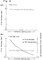
- Fig. 6(a) is a graph of film thickness distribution over the uniformly heating area, and clearly shows the uniformity of the film thickness.
- a ZnS:Mn film was prepared using the same apparatus.
- the deposition conditions were the same, provided that an Mn gas source was fed.
- the Mn gas was introduced in the form of MnCl 2 gas prepared by heating Mn at 800° to 900°C and then mixing with HCl gas to react as follows: Mn (S) + 2HCl (g) ⁇ MnCl 2(g) + H 2(g)
- Fig. 6(b) is a graph which indicates an Mn concentration and a ZnS:Mn film thickness distribution in the uniformly heating area. The results show that the film thickness reduced to 1/3, but has good uniformity.
- the Mn concentration varies widely from relatively high in the upstream region to relatively low in the downstream region.
- the ZnS:Mn film has a wurtzite structure. It is believed that the reduction of the film thickness is caused by etching of the ZnS film by means of HCl gas which occurs by the addition of the MnCl 2 gas.
- the ZnS:Mn film obtained by the reduced-pressure CVD method has a drawback of non-uniformity in the Mn concentration.
- the above results are obtained by a horizontal furnace, but if it is conducted by a perpendicular furnace, the same non-uniformity of Mn concentration would occur.
- the reason for the non-uniformity of Mn concentration is as follows: Since a vapor pressure of MnCl 2 is low in the substrate temperature area, the deposition of Mn occurs easily, so that the Mn in the source material gas is consumed more in the upstream region and the Mn concentration therefore reduces in the downstream region.
- the non-uniformity may be improved by increasing the flow rate of the source material gas, but the source material gas is sufficiently fed in view of the uniformity of the ZnS:Mn film thickness. If the flow rate of the source material gas is increased, a conversion rate of the source material to the deposited film is also reduced and a production cost becomes expensive.
- the increase of the flow raises the inside pressure of the reaction tube, which often gives rise to a non-uniformity caused by the increase of diffusion constant and adversely affects the uniformity of the ZnS film which is a host material of the ZnS:Mn film.
- the present invention may provide an improvement of the chemical vapor deposition (CVD) process for preparing an electroluminescent device having a large area and a large size.
- a process in an embodiment of the present invention comprises forming a luminescent layer on a substrate by reduced-pressure chemical vapor deposition method wherein a source material gas is introduced into a reaction chamber; an improvement being present in that;
- the screening means is not limited as long as the flow of the source material gas is screened in the substrate area. It can be formed by surrounding the substrate area with boards. It also can be a container box having some apertures and put on the substrates area.
- the apertures in the screening means are formed such that the screening effect of the source material gas flow is not lowered.
- the shape and position of the apertures can be determined in view of a concentration of the luminescent center atom in the source material gas.
- the shape includes holes, slits or mesh.
- the shape and position of the apertures are controlled such that at the higher concentration area the apertures are smaller and at the lower concentration area they are larger, whereby the amount of diffusion of the luminescent center atoms through the apertures is substantially equal at any position.
- the apertures and screening means are designed such that the amount of the luminescent center atoms is common around all the substrates.
- the substrates are placed in the second area in which the source material gas flow is little present.
- the feed of the source material gas is mainly conducted by diffusion through the apertures and little by gas stream. Accordingly, the luminescent film is made from the source material fed by the diffusion, so that the concentration of the luminescent center atom can be made uniform.
- Fig. 1 schematically shows an apparatus employed in this example.
- FIG. 2 schematically shows an exploded view of the container 11 of Figure 1.
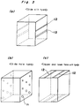
- Fig. 3(a), (b) and (c) show schematical views of other embodiments of the container.
- Fig. 4 shows a graph of L-V (luminance - applied voltage) characteristics with respect to the above obtained EL device and another conventional EL device which was prepared by the electron beam deposition.
- Fig. 5(a) schematically shows an apparatus for chemical vapor deposition (CVD) and Fig. 5(b) schematically shows a substrate holder.
- CVD chemical vapor deposition
- Fig. 6(a) is a film thickness distribution in the uniformly heating area
- Fig. 6(b) is a graph which indicates an Mn concentration and a ZnS:Mn film thickness distribution in the uniform by heating area.
- a source material ZnS
- H 2 a carrier gas
- Mn metal was heated to about 800° to 900°C in a source furnace 10, to which HCl gas was introduced and reacted as follows; Mn (S) + 2HCl (g) ⁇ MnCl 2(g) + H 2(g)
- the resulting MnCl 2 gas was introduced through a supply tube 2 into the reaction chamber 4.
- the introduction of the source material gas could be done by direct introduction of ZnCl 2 gas, H 2 S gas, MnCl 2 gas and the like.
- a substrate 8 was a glass substrate (14 cm x 17 cm) on which a transparent electrode of ITO was formed to about 150 nm (1,500 angstrom) thickness, and thereon a SiO 2 film and Si 3 N 4 film were formed to a total of about 250 nm (2,500 angstrom) thickness. Twenty such substrates 8 were placed in a container box 11 having slits 12, of which an enlarged and schematical view is shown in Fig. 2. The container box 11 had base dimensions of 10 cm x 10 cm and a height of 20.6 cm.
- the container box 11 was placed on a substrate holder 7 and the substrates 8 therein were heated by a substrate furnace 5 to a temperature of 450° to 600°C.
- the pressure inside the reaction tube 4 was kept at about 10°N/m 2 (10 -2 torr). Deposition was conducted at a substrate temperature of about 550°C for 60 minutes.
- the measurement was conducted at 6 points on the luminescent layer (10 cm x 13 cm). As can be seen from Table 1, growth rate was reduced about 5%, but film thickness and Mn concentration distribution were improved. In particular, Mn concentration distribution was significantly improved. Since an optimum Mn concentration of a ZnS:Mn device lies generally within the range of 0.3 to 0.5 atomic %, the film obtained by the above example of the present invention was in this optimum range and no difference in regard with the physical properties of the ZnS:Mn film was observed between the substrates.
- the ZnS:Mn film prepared by the electron beam deposition method has a region of low efficiency from the substrate to 300nm (3,000 angstrom), but in the film produced in accordance with the present invention such a region of low efficiency is less than 100 nm (1,000 angstrom) thick according to the observation of SEM. This difference of the film structure provides a high luminance at low voltage and high saturated luminescence.
- the shape and size of the container 11 can be varied according to the shape and size of the substrate 8 and film-forming conditions.
- the apertures are slits, but holes 20 can be used instead.
- the slits may be formed in the upper and lower surfaces of the container.
- Fig. 3(a), (b) and (c) show schematical views of the above described apertures.
- the invention is not limited to these forms of apertures.
- the form and arrangement of apertures may be determined such that the source material gas is constantly fed.
- a ZnS:Mn film was produced, but other films, such as ZnS:Tb, CaS:Eu and SrSl:Ce can be produced by the above method.
- a thin film EL device having a large area can be produced on an industrial scale. Also the process of the present invention has highly efficient utilization of the source material gas and lowers production costs.
Landscapes
- Chemical & Material Sciences (AREA)
- General Chemical & Material Sciences (AREA)
- Chemical Kinetics & Catalysis (AREA)
- Engineering & Computer Science (AREA)
- Materials Engineering (AREA)
- Mechanical Engineering (AREA)
- Metallurgy (AREA)
- Organic Chemistry (AREA)
- Inorganic Chemistry (AREA)
- Electroluminescent Light Sources (AREA)
Claims (16)
- Procédé CVD (dépôt chimique en phase vapeur) sous pression réduite pour le dépôt d'une couche de matière sur un substrat (8) comprenant les étapes consistant:à provoquer l'écoulement d'un gaz de matière source à travers une chambre de réaction (4); à placer le substrat (8) à l'intérieur d'une zone (19) de ladite chambre de réaction dans laquelle il n'existe pratiquement pas d'écoulement de gaz, et à diffuser le gaz de matière source dans la zone (19) par l'intermédiaire de moyens formant ouvertures (12, 20), caractérisé en ce que les moyens formant ouvertures (12, 20) ont une faible surface dans une région de forte concentration dudit gaz de matière source à l'extérieur de la zone (19) et une grande surface dans une région de faible concentration dudit gaz de matière source à l'extérieur de la zone (19) de telle sorte que la concentration dudit gaz de matière source dans ladite zone soit sensiblement uniforme.
- Procédé selon la revendication 1, dans lequel la couche est une couche luminescente et ledit gaz de matière source comprend un élément de centre luminescent, la concentration de l'élément de centre luminescent étant sensiblement uniforme dans ladite zone.
- Procédé selon la revendication 2, dans lequel ledit gaz de matière source est du gaz MnCl2.
- Procédé selon la revendication 3, comprenant la réaction de Mn avec du gaz HCl pour produire ledit gaz MnCl2.
- Procédé selon l'une quelconque des revendications précédentes, comprenant l'introduction d'un autre gaz dans la chambre de réaction (4).
- Procédé selon la revendication 5, dans lequel l'autre gaz comprend:ZnS et un gaz porteur sélectionné dans le groupe H2, He ou Ar.
- Procédé selon la revendication 5, dans lequel ledit autre gaz comprend:le gaz ZnCl2 et le gaz H2S.
- Dispositif électroluminescent à couche mince produit par un procédé selon l'une quelconque des revendications précédentes.
- Dispositif selon la revendication 8, lorsqu'elle dépend de la revendication 2, comportant une couche luminescente de ZnS:Mn, ZnS:Tb, CaS:Eu ou SeS:Ce.
- Appareil pour réaliser le procédé CVD sous pression réduite pour le dépôt d'une couche de matière sur un substrat (8), ledit appareil comprenant une chambre de réaction (4), des moyens (2) pour introduire dans ladite chambre de réaction un gaz de matière source qui, en service, s'écoule à travers ladite chambre de réaction, et des moyens (11) définissant à l'intérieur de ladite chambre une zone (19) dans laquelle, en service, est enfermé ledit substrat (8) et pratiquement aucun écoulement de gaz n'existe, lesdits moyens définissant la zone comprenant des moyens formant ouvertures (12, 20), par l'intermédiaire desquels il y a diffusion du gaz de matière de source, caractérisé en ce que les moyens formant ouvertures (12, 20) ont une faible surface dans une région dans laquelle la concentration dudit gaz de matière source à l'extérieur de la zone (19) est élevée, et une surface importante dans une région dans laquelle la concentration dudit gaz de matière source à l'extérieur de la zone (19) est faible, de manière à obtenir une concentration sensiblement uniforme dudit gaz de matière source dans ladite zone.
- Appareil selon la revendication 10, dans lequel les moyens formant ouvertures (12, 20) fournissent une région d'ouverture pour la diffusion du gaz, cette région étant plus importante en aval qu'en amont, par rapport à la direction de l'écoulement du gaz de matière.
- Appareil selon la revendication 11, dans lequel les moyens formant ouvertures comprennent des fentes de largeurs différentes (12) qui s'étendent en travers de ladite direction de l'écoulement.
- Appareil selon la revendication 11, dans lequel les moyens formant ouvertures se composent d'orifices (20).
- Appareil selon l'une quelconque des revendications 10 à 13, dans lequel lesdits moyens de définition de zone sont constitués par un récipient (11) formé en plaçant un moyen formant entretoise (16) entre un tube rectangulaire (14) et une boîte inférieure (13), puis en plaçant sur ceux-ci un autre moyen formant entretoise (17) et une boîte supérieure (15).
- Appareil selon l'une quelconque des revendications 10 à 14, dans lequel les moyens (2) pour introduire le gaz de matière source est conçu de façon à introduire ledit gaz de matière source comprenant un élément de centre luminescent.
- Utilisation d'un appareil tel que revendiqué dans la revendication 15 pour produire ladite couche de matière comprenant une couche luminescente ayant une concentration sensiblement uniforme dudit élément de centre luminescent sur le substrat (8).
Applications Claiming Priority (2)
| Application Number | Priority Date | Filing Date | Title |
|---|---|---|---|
| JP2003190A JPH0793191B2 (ja) | 1990-01-09 | 1990-01-09 | 薄膜el素子の製造方法 |
| JP3190/90 | 1990-01-09 |
Publications (2)
| Publication Number | Publication Date |
|---|---|
| EP0437355A1 EP0437355A1 (fr) | 1991-07-17 |
| EP0437355B1 true EP0437355B1 (fr) | 1996-06-05 |
Family
ID=11550487
Family Applications (1)
| Application Number | Title | Priority Date | Filing Date |
|---|---|---|---|
| EP91300159A Expired - Lifetime EP0437355B1 (fr) | 1990-01-09 | 1991-01-09 | Procédé et appareillage pour fabriquer un dispositif électroluminescent à film mince |
Country Status (5)
| Country | Link |
|---|---|
| US (1) | US5147683A (fr) |
| EP (1) | EP0437355B1 (fr) |
| JP (1) | JPH0793191B2 (fr) |
| DE (1) | DE69119916T2 (fr) |
| FI (1) | FI101585B1 (fr) |
Families Citing this family (7)
| Publication number | Priority date | Publication date | Assignee | Title |
|---|---|---|---|---|
| US5300316A (en) * | 1991-12-11 | 1994-04-05 | Kabushiki Kaisha Komatsu Seisakusho | Method of forming thin oxysulfide film |
| US6689422B1 (en) * | 1994-02-16 | 2004-02-10 | Howmet Research Corporation | CVD codeposition of A1 and one or more reactive (gettering) elements to form protective aluminide coating |
| JP3564737B2 (ja) * | 1994-06-24 | 2004-09-15 | 株式会社デンソー | エレクトロルミネッセンス素子の製造方法および製造装置 |
| US5989733A (en) * | 1996-07-23 | 1999-11-23 | Howmet Research Corporation | Active element modified platinum aluminide diffusion coating and CVD coating method |
| EP2001027B1 (fr) | 2003-09-17 | 2013-01-23 | Konica Minolta Medical & Graphic, Inc. | Panneau de conversion d'image radiographique et son procédé de fabrication |
| CN103289693A (zh) * | 2012-02-28 | 2013-09-11 | 海洋王照明科技股份有限公司 | 铈铽共掺杂硼磷酸盐发光材料、制备方法及其应用 |
| CN107604340B (zh) * | 2017-08-31 | 2023-09-01 | 安徽光智科技有限公司 | 化学气相沉积炉 |
Family Cites Families (3)
| Publication number | Priority date | Publication date | Assignee | Title |
|---|---|---|---|---|
| US4582720A (en) * | 1982-09-20 | 1986-04-15 | Semiconductor Energy Laboratory Co., Ltd. | Method and apparatus for forming non-single-crystal layer |
| US4548159A (en) * | 1984-07-06 | 1985-10-22 | Anicon, Inc. | Chemical vapor deposition wafer boat |
| JPH0760738B2 (ja) * | 1988-05-13 | 1995-06-28 | シャープ株式会社 | エレクトロルミネッセンス発光膜の製造方法 |
-
1990
- 1990-01-09 JP JP2003190A patent/JPH0793191B2/ja not_active Expired - Lifetime
-
1991
- 1991-01-08 US US07/638,841 patent/US5147683A/en not_active Expired - Lifetime
- 1991-01-08 FI FI910095A patent/FI101585B1/fi active
- 1991-01-09 EP EP91300159A patent/EP0437355B1/fr not_active Expired - Lifetime
- 1991-01-09 DE DE69119916T patent/DE69119916T2/de not_active Expired - Fee Related
Also Published As
| Publication number | Publication date |
|---|---|
| FI910095A7 (fi) | 1991-07-10 |
| JPH0793191B2 (ja) | 1995-10-09 |
| FI101585B (fi) | 1998-07-15 |
| DE69119916T2 (de) | 1996-11-28 |
| FI101585B1 (fi) | 1998-07-15 |
| JPH03208298A (ja) | 1991-09-11 |
| DE69119916D1 (de) | 1996-07-11 |
| FI910095A0 (fi) | 1991-01-08 |
| US5147683A (en) | 1992-09-15 |
| EP0437355A1 (fr) | 1991-07-17 |
Similar Documents
| Publication | Publication Date | Title |
|---|---|---|
| EP0464515B1 (fr) | Procédé pour fabriquer un film à nitride de silicium | |
| US6297522B1 (en) | Highly uniform silicon carbide epitaxial layers | |
| US5294286A (en) | Process for forming a thin film of silicon | |
| US4735822A (en) | Method for producing an electronic device having a multi-layer structure | |
| US5334250A (en) | Vapor deposition apparatus for using solid starting materials | |
| US5593497A (en) | Method for forming a deposited film | |
| US5356657A (en) | Method of manufacturing an electroluminescent device | |
| EP0437355B1 (fr) | Procédé et appareillage pour fabriquer un dispositif électroluminescent à film mince | |
| US5390626A (en) | Process for formation of silicon carbide film | |
| US5750188A (en) | Method for forming a thin film of a non-stoichiometric metal oxide | |
| US5185181A (en) | Process for preparing an electroluminescent thin film | |
| US5135607A (en) | Process for forming deposited film | |
| EP0242182B1 (fr) | Procédé pour former une couche déposée | |
| US5275840A (en) | Manufacturing method for electroluminescent thin film | |
| EP0240314B1 (fr) | Procédé pour la formation d'un film déposé | |
| US5372839A (en) | Process for preparing an electroluminescent film | |
| EP0241311B1 (fr) | Procédé pour former une couche déposée | |
| EP0243074B1 (fr) | Procédé de fabrication d'une couche déposée | |
| EP1100978A1 (fr) | Procede et appareil de formation de films d'alliage silicium/germanium amorphes et polycristallins | |
| EP0240305A2 (fr) | Méthode de fabrication d'une couche déposée | |
| JPH02119126A (ja) | 半導体装置作製方法 | |
| JPH02152191A (ja) | エレクトロルミネッセンス発光膜の気相成長法 | |
| JPH01766A (ja) | 半導体装置 | |
| JPH07315826A (ja) | 多結晶シリコン薄膜及びその製造方法 | |
| JP2726353B2 (ja) | エレクトロルミネッセンス薄膜の成長方法 |
Legal Events
| Date | Code | Title | Description |
|---|---|---|---|
| PUAI | Public reference made under article 153(3) epc to a published international application that has entered the european phase |
Free format text: ORIGINAL CODE: 0009012 |
|
| AK | Designated contracting states |
Kind code of ref document: A1 Designated state(s): DE FR GB |
|
| 17P | Request for examination filed |
Effective date: 19910801 |
|
| 17Q | First examination report despatched |
Effective date: 19940214 |
|
| GRAA | (expected) grant |
Free format text: ORIGINAL CODE: 0009210 |
|
| AK | Designated contracting states |
Kind code of ref document: B1 Designated state(s): DE FR GB |
|
| REF | Corresponds to: |
Ref document number: 69119916 Country of ref document: DE Date of ref document: 19960711 |
|
| ET | Fr: translation filed | ||
| GRAH | Despatch of communication of intention to grant a patent |
Free format text: ORIGINAL CODE: EPIDOS IGRA |
|
| PLBE | No opposition filed within time limit |
Free format text: ORIGINAL CODE: 0009261 |
|
| STAA | Information on the status of an ep patent application or granted ep patent |
Free format text: STATUS: NO OPPOSITION FILED WITHIN TIME LIMIT |
|
| 26N | No opposition filed | ||
| PGFP | Annual fee paid to national office [announced via postgrant information from national office to epo] |
Ref country code: DE Payment date: 20010102 Year of fee payment: 11 |
|
| PGFP | Annual fee paid to national office [announced via postgrant information from national office to epo] |
Ref country code: GB Payment date: 20010103 Year of fee payment: 11 |
|
| PGFP | Annual fee paid to national office [announced via postgrant information from national office to epo] |
Ref country code: FR Payment date: 20010125 Year of fee payment: 11 |
|
| REG | Reference to a national code |
Ref country code: GB Ref legal event code: IF02 |
|
| PG25 | Lapsed in a contracting state [announced via postgrant information from national office to epo] |
Ref country code: GB Free format text: LAPSE BECAUSE OF NON-PAYMENT OF DUE FEES Effective date: 20020109 |
|
| PG25 | Lapsed in a contracting state [announced via postgrant information from national office to epo] |
Ref country code: DE Free format text: LAPSE BECAUSE OF NON-PAYMENT OF DUE FEES Effective date: 20020801 |
|
| GBPC | Gb: european patent ceased through non-payment of renewal fee |
Effective date: 20020109 |
|
| PG25 | Lapsed in a contracting state [announced via postgrant information from national office to epo] |
Ref country code: FR Free format text: LAPSE BECAUSE OF NON-PAYMENT OF DUE FEES Effective date: 20020930 |
|
| REG | Reference to a national code |
Ref country code: FR Ref legal event code: ST |