EP0437376A2 - Phasenverschiebungsmaske und Verfahren zur Herstellung - Google Patents
Phasenverschiebungsmaske und Verfahren zur Herstellung Download PDFInfo
- Publication number
- EP0437376A2 EP0437376A2 EP91300207A EP91300207A EP0437376A2 EP 0437376 A2 EP0437376 A2 EP 0437376A2 EP 91300207 A EP91300207 A EP 91300207A EP 91300207 A EP91300207 A EP 91300207A EP 0437376 A2 EP0437376 A2 EP 0437376A2
- Authority
- EP
- European Patent Office
- Prior art keywords
- phase shifting
- light shielding
- forming
- light
- resist pattern
- Prior art date
- Legal status (The legal status is an assumption and is not a legal conclusion. Google has not performed a legal analysis and makes no representation as to the accuracy of the status listed.)
- Granted
Links
Images


Classifications
-
- G—PHYSICS
- G03—PHOTOGRAPHY; CINEMATOGRAPHY; ANALOGOUS TECHNIQUES USING WAVES OTHER THAN OPTICAL WAVES; ELECTROGRAPHY; HOLOGRAPHY
- G03F—PHOTOMECHANICAL PRODUCTION OF TEXTURED OR PATTERNED SURFACES, e.g. FOR PRINTING, FOR PROCESSING OF SEMICONDUCTOR DEVICES; MATERIALS THEREFOR; ORIGINALS THEREFOR; APPARATUS SPECIALLY ADAPTED THEREFOR
- G03F1/00—Originals for photomechanical production of textured or patterned surfaces, e.g., masks, photo-masks, reticles; Mask blanks or pellicles therefor; Containers specially adapted therefor; Preparation thereof
- G03F1/26—Phase shift masks [PSM]; PSM blanks; Preparation thereof
- G03F1/29—Rim PSM or outrigger PSM; Preparation thereof
Definitions
- This invention relates to phase shifting masks and to methods of manufacturing such masks, which can be used in the formation of a variety of patterns, such as resist patterns in the process of manufacturing semiconductor devices.
- phase shifting method is disclosed, for example, in Japanese Patent Laid-open No. Sho 58 (1983)-173744; in Marc D. Levenson et al., "Improving Resolution in Photolithography with a Phase Shifting Mask", IEEE Transactions on Electron Devices, Vol. ED-29, No. 12, December 1982, pp. 1828 - 1836; and in Marc D. Levenson et al., "The Phase Shifting Mask II; Imaging Simulations and Submicrometer Resist Exposures", Transactions on Electron Devices, Vol. ED-31, No. 6, June 1984, pp. 753 - 763.
- a light shielding region 10 is formed by the use of a light shielding material such as chromium on a transparent substrate 1 of quartz or the like, and an arrangement of repeated line-and-space patterns is formed to produce an exposure mask.
- the intensity distribution of the light transmitted through such an exposure mask is represented by a curve A1 in Figure 1(a), wherein the intensity is zero at the light shielding regions 10 while the light is transmitted through the other regions (light transmitting segments 12a, 12b) to provide constant light intensity levels.
- the intensity of the light transmitted therethrough and irradiated on a work member to be exposed is distributed as represented by a curve A2 in Figure 1(a), wherein hill-like maxima have flatter regions on either side due to the diffraction of the light.
- the light passing through the light transmitting segment 12b is represented by a one-dot chained line which is similar to, but dimensionally displaced from, the curve A2.
- phase shifting films are provided on the light transmitting segments of the repeated patterns alternately as shown in Figure 1(b), any blur of the image resulting from diffraction of the light is eliminated by inversion of the phase resulting in a sharp image and thereby improving the resolution and the focusing performance. More particularly, when a phase shifting film 11a is formed on the light transmitting segment 12a as shown in Figure 1(b) in such a manner as to cause a phase shift of 180° for example, the light passed through the phase shifting film 11a is inverted, as represented by a curve B1. The light obtained through the adjacent light transmitting segment 12a does not pass through a phase shifting film so that there is no such phase inversion.
- a member used for reduced-size projection may be termed a reticle, and a member for actual-size projection may then be termed a mask; alternatively a member corresponding to an original sheet may be termed a reticle, and a member obtained by duplicating such a reticle may then be termed a mask.
- a mask any one of the masks and reticles classified by such various definitions is generally termed a mask.
- phase shifting mask utilising the previously-proposed phase shifting mask is very effective for forming an arrangement of repeated patterns such as the line-and-space patterns shown in Figure 1(b), there still exists a problem that such a mask is not readily usable in forming isolated patterns which are not repetitive.
- the phase shifting technique causes a phase difference between the light beams for exposure of mutually adjacent patterns, and utilises the effect that the respective overlapping light intensities cancel each other.
- mutually proximate light beams are not present in the case of forming an isolated line or a contact hole, the above phase shifting technique is not directly applicable.
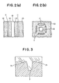
- phase shifting segments 11 are formed along the two sides of and in the proximity of a rectangularly extending light transmitting region 12 which is a main space in the mask of Figure 2(a) for forming an isolated line pattern; alternatively the segments 11 are formed along and in the proximity of four sides of a square light transmitting region 12 in the mask of Figure 2(b) for forming a hole pattern.
- phase shifting segment 11 needs to have certain dimensions since the effect thereof is diminished in accordance with a dimensional decrease. As a result, there arises another problem in that the pattern of the phase shifting segment 11 is itself transferred.
- Figure 3 illustrates an exemplary case in which an isolated space 7 is formed by using the mask of Figure 2(a). As shown with some exaggeration in Figure 3, it is unavoidable that patterns 71 derived directly from the phase shifting segments 11 are also formed.
- a phase shifting mask comprising, on a substrate, a transparent region which is transparent to exposure light and a light shielding region for shielding the exposure light, said transparent region having a light transmitting segment for directly transmitting the exposure light therethrough and a phase shifting segment for transmitting the exposure light therethrough with a phase difference from the light transmitted through said light transmitting segment,
- said light shielding region is formed adjacent at least said phase shifting segment or said light transmitting segment, and said phase shifting segment and said light transmitting segment are formed adjacent each other.
- a method of manufacturing a phase shifting mask comprising the steps of: forming a light shielding layer on a substrate; forming a photoresist on said light shielding layer; patterning said photoresist to form a resist pattern; forming an opening in said light shielding layer by the use of said resist pattern as a mask, thereby forming a light shielding pattern; etching said substrate anisotropically to form a phase shifting segment; side etching said light shielding pattern to form a light shielding region; and removing said resist pattern.
- a method of manufacturing a phase shifting mask comprising the steps of: forming a light shielding layer on a substrate; forming a photoresist on said light shielding layer; patterning said photoresist to form a resist pattern; forming an opening in said light shielding layer by the use of said resist pattern as a mask, thereby forming a light shielding pattern; etching said substrate anisotropically to form a phase shifting segment; removing said resist pattern; and etching said light shielding pattern isotropically to form a light shielding region.
- a method of manufacturing a phase shifting mask comprising the steps of: forming a light shielding layer on a substrate; forming a photoresist on said light shielding layer; patterning said photoresist to form a resist pattern; forming an opening in said light shielding layer by the use of said resist pattern as a mask, thereby forming a light shielding pattern; side etching said light shielding pattern to form a light shielding region; depositing a phase shifting material in said opening by the use of said resist pattern as a mask; and removing said resist pattern together with phase shifting material thereon to form a phase shifting segment in said opening.
- a method of manufacturing a phase shifting mask comprising the steps of: forming a light shielding layer on a substrate; forming a photoresist on said light shielding layer; patterning said photoresist to form a first resist pattern; forming an opening in said light shielding layer by the use of said first resist pattern as a mask, thereby forming a light shielding pattern; removing said first resist pattern; forming a photoresist on said light shielding pattern and said opening; removing said photoresist partially from said opening thereby forming a second resist pattern; anisotropically etching said substrate in a partial area of said opening thereby forming a phase shifting region; and removing said second resist pattern.
- a method of manufacturing a phase shifting mask comprising the steps of: forming a light shielding layer on a substrate; forming a photoresist on said light shielding layer; patterning said photoresist to form a first resist pattern; forming an opening in said light shielding layer by the use of said first resist pattern as a mask, thereby forming a light shielding pattern; removing said first resist pattern; forming a layer of a phase shifting material on said light shielding pattern and said opening; forming a photoresist on said layer of the phase shifting material; removing said photoresist in such a manner as to leave a second opening which is positioned over and is narrower than the first-mentioned opening, thereby forming a second resist pattern; anisotropically etching said layer of the phase shifting material by the use of said second resist pattern as a mask, thereby forming a phase shifting region; and removing said second resist pattern.
- a method of manufacturing a phase shifting mask comprising the steps of: forming a light shielding layer on a substrate; forming a photoresist on said light shielding layer; patterning said photoresist to form a first resist pattern; forming an opening in said light shielding layer by the use of said first resist pattern as a mask, thereby forming a light shielding pattern; removing said first resist pattern; forming a photoresist on said light shielding pattern and said opening; removing said photoresist partially from said opening thereby forming a second resist pattern; depositing a phase shifting material in said opening partially by the use of said second resist pattern as a mask; and removing said second resist pattern together with said phase shifting material thereon to leave a phase shifting segment in a partial area of said opening.
- Embodiments of the present invention described in greater detail hereinafter provide an improved phase shifting mask which can have a reduced pattern-forming area thereby decreasing the space required while preventing transfer of any unrequired pattern of a phase shifting film even when forming an isolated line (space) or a hole pattern.
- the embodiments of the present invention also provide improved methods of manufacturing a phase shifting mask, which are capable of minimising the number of required steps, particularly by overcoming the necessity of executing a plotting step twice to obtain a mask of a desired structure.
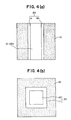
- phase shifting masks embodying the present invention each comprise a transparent region 20 (transparent with respect to exposure light) and a light shielding region 10.
- the transparent region 20 has a light transmitting segment 12 for directly transmitting the exposure light therethrough, and phase shifting segments 11, 11a, 11b for transmitting the exposure light therethrough with a phase difference from the light transmitted through the light transmitting segment 12.
- the light shielding region 10 is formed so as to be adjacent at least the phase shifting segments 11, 11a, 11b or the light transmitting segment 12.
- the light transmitting segment 12 may be composed so as to permit transmission of the exposure light without any phase shift.
- the light shielding region 10 is positioned adjacent the phase shifting segments 11, 11a, 11b.
- the arrangement may be modified so that the light shielding region 10 is adjacent the light transmitting segment 12. More specifically, in the example of Figure 4(a), two rows of phase shifting segments 11a, 11b are formed adjacent respective sides of a light transmitting segment 12 corresponding to an isolated line (space) pattern, and the phase shifting segments 11a, 11b are positioned adjacent the surrounding light shielding region 10.
- phase shifting segment of a shape corresponding to a desired pattern may be formed at the centre, and rows of light transmitting segments may be formed on respective sides of the phase shifting segment region, in such a manner that the light transmitting segments and the light shielding region 10 adjoin mutually.
- a phase shifting segment 11 is formed adjacent a light transmitting segment 12 which corresponds to a desired hole pattern, in a manner to surround the four sides of the light transmitting segment 12, and the phase shifting segment 11 adjoins the peripheral light shielding region 10.
- this arrangement may be modified so that a phase shifting segment of a shape corresponding to a desired hole pattern is formed at the centre, while a light transmitting segment is formed in a manner which surrounds the phase shifting segment, and the light transmitting segment and the light shielding segment 10 adjoin mutually.
- a transparent region 20 on a mask is generally divided into two mutually adjacent segments, and these segments are composed so as to cause a phase difference between exposure light transmitted therethrough.
- the effect thereby achieved is optimised when the phase difference is 180°.
- the light transmitted through the periphery of the central area (light transmitting segment 12 in Figures 4(a) and 4(b)) of the transparent region 20 is cancelled by the light transmitted through the outer difference-phase areas (phase shifting segments 11, 11a, 11b in Figures 4(a) and 4(b)), so that the intensity of the former light is rendered lower than the intensity obtained in a different structure where the central area (light transmitting segment 12) alone is present. Therefore, the resultant pattern becomes considerably smaller as compared to the pattern exposed and transferred in the structure where merely the central area (light transmitting segment 12) is present.
- the central area (light transmitting segment 12) is formed to be greater than the size of the desired pattern to be obtained so that it becomes possible to transfer a pattern of the desired size. Also, the resolution of the pattern thus obtained can be enhanced due to the effect of the phase shifting process.
- This example represents a case in which there is formed a contact hole of a 0.15- ⁇ m square by using a KrF excimer laser (light wavelength 248 nm).
- the space can be minimised without inducing transfer of any unrequired pattern, hence ensuring a high resolution.
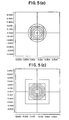
- FIG. 6(a) to 6(c) graphically shows the light intensity distribution obtained on an exposed work member such as a wafer by the use of a KrF excimer laser in transferring an isolated line pattern of 0.25 ⁇ m in width.
- the abscissa represents length in ⁇ m
- the ordinate represents an absolute value of the light intensity on the exposed work member with the irradiated light regarded as unity.
- Figure 6(a) graphically shows the result obtained relative to a previously-proposed mask without using the phase shifting technique, wherein the light intensity distribution Ia on the exposed work member is curved in conformity with the irradiated light IIa passed through the light transmitting segment of the mask.
- the maximum light intensity in the distribution Ia on the exposed work member was 0.5299.
- Figure 6(b) graphically shows the result obtained by a previously-proposed phase shifting mask according to Figure 2(a).
- the intensity distribution Ib1 of the pattern exposure light corresponding to the irradiated light IIb1 through the light transmitting segment 12 in Figure 2(a) indicates a major maximum intensity of 0.6640.
- a sub-peak is generated in the intensity distribution Ib2 of the irradiated light IIb2 through the phase shifting segment 11, and its maximum value of 0.2902 is considerable. This signifies that the possibility of transfer of an unrequired pattern is high.
- phase shifting masks such as those of Figures 4(a) and 4(b), will now be described.
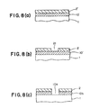
- a first embodiment comprises the following steps as illustrated in Figures 7(a) to 7(f).
- An opening is provided in a light shielding layer to form a light shielding pattern, and then the light shielding pattern is processed by side-etching while being marked with a photoresist to form a light shielding region of the phase shifting mask.
- a film of a material having light shielding properties is formed as a light shielding layer 10′ on a substrate 1 (of silicon dioxide or the like) having light transmitting properties; and a photoresist 2′ is formed as a film on the light shielding layer 10′ by coating or the like thereby to produce a structure as shown in Figure 7(a).
- a material having light shielding properties for example, chromium or any other material such as a heavy metal or oxide thereof suited to shield exposure light
- a photoresist 2′ is formed as a film on the light shielding layer 10′ by coating or the like thereby to produce a structure as shown in Figure 7(a).
- an electron beam (EB) plotting step is executed, and the photoresist 2′ is patterned thereby to form a resist pattern 2 with a resist opening 21, as illustrated in Figure 7(b).
- EB electron beam
- a light shielding pattern 10b with an opening 10a is obtained by the normal technique of photolithography while being masked with the resist pattern 2, as illustrated in Figure 7(c). Since the opening 10a corresponds to the phase shifting segment 12 (see Figure 7(f)) of a final desired structure, both the opening 10a and the resist opening 21 are formed in conformity therewith.
- the resist pattern 2 is obtained by EB-plotting and developing the resist 2′, and the light shielding layer 10′ is patterned by etching or the like while being masked with the resist pattern 2.
- the processing steps are the same as those adopted in manufacture of an ordinary reticle, and therefore known techniques may be employed.
- the substrate 1 is etched while being masked directly with the resist pattern 2, whereby a recess 1a is formed in the substrate as illustrated in Figure 7(d).
- the phase shifting effect is maximised when the above condition is satisfied.
- the light shielding pattern 10b is side-etched while being masked with the resist pattern 2, whereby a structure as shown in Figure 7(e) is obtained, with a light shielding region 10 in which the light shielding pattern 10b is partially etched on both sides of the recess 1a in the substrate 1. Portions 10c, 10d are removed from the light shielding pattern 10b by the etching in this step.
- side etching signifies etching in a lateral direction (leftward-rightward lateral direction in the drawing) orthogonal to the depth of the light shielding pattern 10b (upward-downward vertical direction in the drawing).
- Such side etching can be executed with a suitable agent which causes an erosive action on the material of the light shielding pattern 10b.
- the side etching can be effected in a wet etching mode with a selected etching liquid which meets the above requirement. Since the side-etched portions 10c, 10d correspond to the light transmitting segments 11a, 11b respectively as illustrated in Figure 7(e), the amount of such etching is determined in conformity with the desired size.
- phase shifting mask structure as shown in Figure 7(f), which comprises a transparent region 20 with respect to exposure light and a light shielding region 10 for shielding the exposure light, wherein the transparent region 20 has light transmitting segments 11a, 11b for directly transmitting the exposure light therethrough, and the phase shifting segment 12 for transmitting exposure light therethrough with a phase difference from the light passed through the light transmitting segments.
- the plan-view constitution of the phase shifting mask may be shaped into a contact hole pattern as shown in Figure 4(b) or a line (space) pattern as shown in Figure 4(a).
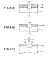
- a light shielding layer 10′ is formed of chromium or the like on a substrate 1 (of quartz, silicon dioxide or the like) having light transmitting properties, as illustrated in Figure 8(a).
- the thickness of the light shielding layer 10′ is selectively determined to be greater than the thickness of a light shielding region 10 which is to be finally obtained.
- a resist 2′ is formed on the light shielding layer 10′ by coating or the like to produce the structure shown in Figure 8(a).
- the light shielding layer 10′ is anisotropically etched while being masked with the resist pattern 2, whereby an opening 10a is formed in the light shielding layer to obtain a structure as shown in Figure 8(c). Since the opening 10a corresponds to the phase shifting segment 12 (see Figure 8(f)) in a desired final structure, both the opening 10a and the resist opening 21 are formed to have proper dimensions conforming therewith.
- the substrate 1 is anisotropically etched while being masked with the resist pattern 2, thereby obtaining a structure as shown in Figure 8(d), having a substrate recess 1a. Since this recess 1a serves as the phase shifting segment 12, the depth d thereof in this embodiment is selected so as to be equal to that of the substrate recess 1a in the first embodiment of Figures 7(a) to 7(f), so as to maximise the phase shifting effect.
- the resist pattern 2 is then removed in order to attain a state as illustrated in Figure 8(e).
- isotropic etching is executed to remove the light shielding layer in the periphery of the recess 1a, thereby producing a structure as shown in Figure 8(f).
- the isotropic etching may be carried out by any means capable of isotropically etching the light shielding material, and a wet etching means may be employed.
- a wet etching means may be employed as the portions to be removed by such isotropic etching serve as the light transmitting segments 11a, 11b, the required amount of etching is determined in conformity therewith.
- the phase shifting mask structure of Figure 8(f) can be obtained, comprising a transparent region 20 (transparent with respect to the exposure light) and a light shielding region 10 for shielding such exposure light, wherein the transparent region 20 has light transmitting segments 11a, 11b for directly transmitting the exposure light therethrough, and the phase shifting segment 12 for transmitting the exposure light therethrough with a phase difference from the light passed through the light transmitting segments.
- a third embodiment shown in Figures 9(d) to 9(f) is arranged so as to form a projection 42 on the substrate 1, the projection 42 being formed from a suitable material having a phase shifting effect, wherein the projection is used as the phase shifting region 12 (see Figure 9(f)).
- a suitable material having a phase shifting effect such as silicon dioxide, is then evaporated by means of chemical vapour deposition (CVD) or the like, thereby forming the projection 42 of phase shifting material of a size corresponding to a resist opening 21 in the resist pattern 2, as illustrated in Figure 9(e). Simultaneously therewith, a film 41 of phase shifting material is formed on the resist pattern 2 as well.
- CVD chemical vapour deposition
- phase shifting mask structure as shown in Figure 9(f) which comprises a light shielding region 10 and a transparent region 20 having a phase shifting segment 12 composed of the phase shifting projection 42 and the light transmitting segments 11a, 11b formed by the side etching step.
- a light shielding film 10′ is formed on a transparent substrate of quartz or the like by evaporation of a light shielding material such as chromium, and a resist film 2′ is formed thereon. Subsequently, an opening 21 of a size corresponding to a desired transparent region 20 (see Figure 10(c)) is formed in the resist film 2′ by normal photolithography thereby obtaining a resist pattern 2 ( Figure 10(b)).
- the light shielding film 10′ is partially removed by etching or the like while being masked with the resist pattern 2, and then the remaining resist pattern is removed to produce a structure as shown in Figure 10(c) which includes a light shielding region 10 and a transparent region 20.
- an opening 31 of a size corresponding to a desired light transmitting segment 12 is formed in the resist 3′ to provide a resist pattern 3 as illustrated in Figure 10(e).
- the substrate 1 is partially etched while being masked by the resist pattern 3 so that, as illustrated in Figure 10(f), the central portion of the transparent region 20 becomes reduced in thickness.
- This central portion serves as a light transmitting segment 12, and its two sides serve as the phase shifting segments 11a, 11b.
- the phases of the transmitted light beams are rendered mutually different by partially changing the thickness of the substrate 1, thereby forming the light transmitting segment 12 and the phase shifting segments 11a, 11b.
- a fifth embodiment shown in Figures 11(d) to 11(f) the steps up to and including forming the light shielding region 10 and the transparent region 20 are the same as those in the fourth embodiment as shown in Figures 10(a) to 10(c).
- a layer 4′ having a phase shifting effect is formed over the surface, and a resist film 5′ is formed thereon.
- An opening 51 corresponding to a light transmitting region 12 ( Figure 11(f)) is then formed in the resist film 5′ by photolithography to produce a resist pattern 5 as shown in Figure 11(e).
- the material 4′ having a phase shifting effect is patterned by etching or the like while being masked with the resist pattern 5.
- a projection 4 of the phase shifting material 4′ is formed in a thickness d on each side of the transparent region 20 to serve as a phase shifting mask.
- the portions where such projection 4 is present on the transparent region 20 are used as phase shifting segments 11a, 11b, while any other portion of the transparent region 20 is used as a light transmitting segment 12.
- the thickness d of the projection 4 is selected so as to be optimal for attaining a desired phase shift.
- the thickness d determined according to the aforementioned equation is selected to cause a phase shift of 180°.
- the phase shifting segments 11a, 11b are composed of a phase shifting film as described above.
- Materials suited for the film may include, in addition to silicon dioxide, organic materials such as polyimide resin or resist material, or inorganic materials such as silicon nitride. It is also possible to use any material that can be processed so as to finally become silicon dioxide by baking, such as SOG.
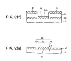
- the early steps correspond to those of Figures 10(a) to 10(e) of the fourth embodiment, such that the structure of Figure 10(e) is obtained with a resist pattern 3 formed on a light shielding region 10.
- a material having a phase shifting effect is deposited as illustrated in Figure 12(f), whereby a projection 6 of the phase shifting material is formed in the portion of the transparent region 20 of the substrate 1 not covered with the resist pattern 3.
- a film 61 of the phase shifting material is formed on the resist pattern 3 as well.
- the resist pattern 3 is then removed such that, as illustrated in Figure 12(g), a phase shifting segment 11 composed of the projection 6 is formed at the centre of the transparent region 20, and light transmitting segments 12a, 12b are formed on both sides of the segment 11.
- the film 61 of the phase shifting material deposited on the resist pattern 3 in the step of Figure 12(f) has already been removed together with the resist pattern 3.
- the sixth embodiment involves a process in reverse whereby the phase shifting segment 11 is formed at the centre of the transparent region 20, and its two sides are used as the light transmitting segments 12a, 12b.
- the thickness d and the material of the projection to be used as a phase shifting segment can be the same as those in the fifth embodiment.
Landscapes
- Physics & Mathematics (AREA)
- General Physics & Mathematics (AREA)
- Exposure And Positioning Against Photoresist Photosensitive Materials (AREA)
- Preparing Plates And Mask In Photomechanical Process (AREA)
- Exposure Of Semiconductors, Excluding Electron Or Ion Beam Exposure (AREA)
Priority Applications (1)
| Application Number | Priority Date | Filing Date | Title |
|---|---|---|---|
| EP96102706A EP0730200A3 (de) | 1990-01-12 | 1991-01-11 | Phasenverschiebungsmaske und Verfahren zur Herstellung |
Applications Claiming Priority (6)
| Application Number | Priority Date | Filing Date | Title |
|---|---|---|---|
| JP5606/90 | 1990-01-12 | ||
| JP560690A JP3122107B2 (ja) | 1990-01-12 | 1990-01-12 | 位相シフトマスクの製造方法 |
| JP69979/90 | 1990-03-20 | ||
| JP2069979A JPH03269531A (ja) | 1990-03-20 | 1990-03-20 | 位相シフトマスクの製造方法 |
| JP2116464A JPH0413141A (ja) | 1990-05-02 | 1990-05-02 | 位相シフトマスクの製造方法 |
| JP116464/90 | 1990-05-02 |
Related Child Applications (1)
| Application Number | Title | Priority Date | Filing Date |
|---|---|---|---|
| EP96102706.7 Division-Into | 1996-02-23 |
Publications (3)
| Publication Number | Publication Date |
|---|---|
| EP0437376A2 true EP0437376A2 (de) | 1991-07-17 |
| EP0437376A3 EP0437376A3 (en) | 1991-11-06 |
| EP0437376B1 EP0437376B1 (de) | 1997-03-19 |
Family
ID=27276824
Family Applications (2)
| Application Number | Title | Priority Date | Filing Date |
|---|---|---|---|
| EP91300207A Expired - Lifetime EP0437376B1 (de) | 1990-01-12 | 1991-01-11 | Phasenverschiebungsmaske und Verfahren zur Herstellung |
| EP96102706A Withdrawn EP0730200A3 (de) | 1990-01-12 | 1991-01-11 | Phasenverschiebungsmaske und Verfahren zur Herstellung |
Family Applications After (1)
| Application Number | Title | Priority Date | Filing Date |
|---|---|---|---|
| EP96102706A Withdrawn EP0730200A3 (de) | 1990-01-12 | 1991-01-11 | Phasenverschiebungsmaske und Verfahren zur Herstellung |
Country Status (3)
| Country | Link |
|---|---|
| EP (2) | EP0437376B1 (de) |
| KR (1) | KR0163437B1 (de) |
| DE (1) | DE69125195T2 (de) |
Cited By (18)
| Publication number | Priority date | Publication date | Assignee | Title |
|---|---|---|---|---|
| DE4031413A1 (de) * | 1990-05-25 | 1991-11-28 | Samsung Electronics Co Ltd | Verfahren zur herstellung einer maske |
| EP0489539A3 (en) * | 1990-12-05 | 1992-09-16 | American Telephone And Telegraph Company | Method of making phase-shifting lithographic masks |
| EP0475694A3 (en) * | 1990-09-10 | 1992-09-16 | Fujitsu Limited | Optical mask using phase shift and method of producing the same |
| EP0477035A3 (en) * | 1990-09-21 | 1992-10-21 | Dai Nippon Printing Co., Ltd. | Phase shift layer-containing photomask, and its production and correction |
| EP0500393A3 (en) * | 1991-02-22 | 1993-01-27 | Canon Kabushiki Kaisha | Imaging method for manufacture of microdevices |
| EP0529338A1 (de) * | 1991-07-30 | 1993-03-03 | Fujitsu Limited | Photomaske und Verfahren zur Herstellung |
| EP0551621A1 (de) * | 1992-01-13 | 1993-07-21 | International Business Machines Corporation | Selbstausrichtende Phasenverschiebungsmaske |
| EP0553543A1 (de) * | 1992-01-31 | 1993-08-04 | Mitsubishi Denki Kabushiki Kaisha | Verfahren zur Erzeugung eines Fotolackmusters |
| EP0595750A1 (de) * | 1992-10-30 | 1994-05-04 | International Business Machines Corporation | Phasenverschiebungsmaske mit abwechselnden Rändern |
| US5345292A (en) * | 1992-03-31 | 1994-09-06 | Canon Kabushiki Kaisha | Illumination device for projection exposure apparatus |
| EP0461778B1 (de) * | 1990-06-15 | 1996-01-03 | Mitsubishi Denki Kabushiki Kaisha | Verfahren zur Herstellung eines Maskenmusters |
| US5489509A (en) * | 1989-04-28 | 1996-02-06 | Fujitsu, Ltd. | Mask, mask producing method and pattern forming method using mask |
| EP0590627A3 (en) * | 1992-09-29 | 1996-08-07 | Texas Instruments Inc | Improved photomask for semiconductor fabrication |
| US5574492A (en) * | 1992-03-27 | 1996-11-12 | Canon Kabushiki Kaisha | Imaging method and semiconductor device manufacturing method using the same |
| US5631773A (en) * | 1991-08-02 | 1997-05-20 | Canon Kabushiki Kaisha | Image projection method and semiconductor device manufacturing method using the same |
| US5673102A (en) * | 1991-02-22 | 1997-09-30 | Canon Kabushiki Kaisha | Image farming and microdevice manufacturing method and exposure apparatus in which a light source includes four quadrants of predetermined intensity |
| US6551750B2 (en) | 2001-03-16 | 2003-04-22 | Numerical Technologies, Inc. | Self-aligned fabrication technique for tri-tone attenuated phase-shifting masks |
| US6635393B2 (en) | 2001-03-23 | 2003-10-21 | Numerical Technologies, Inc. | Blank for alternating PSM photomask with charge dissipation layer |
Families Citing this family (5)
| Publication number | Priority date | Publication date | Assignee | Title |
|---|---|---|---|---|
| US6436608B1 (en) * | 2000-01-20 | 2002-08-20 | Agere Systems Guardian Corp. | Lithographic method utilizing a phase-shifting mask |
| US6638663B1 (en) | 2000-01-20 | 2003-10-28 | Agere Systems Inc. | Phase-shifting mask and semiconductor device |
| AU2001227931A1 (en) | 2000-01-20 | 2001-07-31 | Free-Flow Packaging International, Inc. | System, method and material for making pneumatically filled packing cushions |
| US7282461B2 (en) | 2003-09-04 | 2007-10-16 | Agere Systems, Inc. | Phase-shifting mask and semiconductor device |
| EP2188838B1 (de) | 2007-09-04 | 2015-04-01 | NDS Limited | Sicherheitschip |
Family Cites Families (5)
| Publication number | Priority date | Publication date | Assignee | Title |
|---|---|---|---|---|
| EP0090924B1 (de) * | 1982-04-05 | 1987-11-11 | International Business Machines Corporation | Verfahren zur Erhöhung der Bildauflösung einer Photomaske und Photomaske zur Dürchführung dieses Verfahrens |
| CA1313792C (en) * | 1986-02-28 | 1993-02-23 | Junji Hirokane | Method of manufacturing photo-mask and photo-mask manufactured thereby |
| US5234780A (en) * | 1989-02-13 | 1993-08-10 | Kabushiki Kaisha Toshiba | Exposure mask, method of manufacturing the same, and exposure method using the same |
| EP0653679B1 (de) * | 1989-04-28 | 2002-08-21 | Fujitsu Limited | Maske, Verfahren zur Herstellung der Maske und Verfahren zur Musterherstellung mit einer Maske |
| EP0401795A3 (de) * | 1989-06-08 | 1991-03-27 | Oki Electric Industry Company, Limited | Phasenverschiebungs-Photomaske für negative Lacke und Verfahren zur Herstellung von isolierten negativen Resistbildern mit dieser Phasenverschiebungsmaske |
-
1991
- 1991-01-11 EP EP91300207A patent/EP0437376B1/de not_active Expired - Lifetime
- 1991-01-11 EP EP96102706A patent/EP0730200A3/de not_active Withdrawn
- 1991-01-11 DE DE1991625195 patent/DE69125195T2/de not_active Expired - Fee Related
- 1991-01-11 KR KR1019910000303A patent/KR0163437B1/ko not_active Expired - Fee Related
Cited By (31)
| Publication number | Priority date | Publication date | Assignee | Title |
|---|---|---|---|---|
| US5786115A (en) * | 1989-04-28 | 1998-07-28 | Fujitsu Limited | Mask producing method |
| US5674646A (en) * | 1989-04-28 | 1997-10-07 | Fujitsu Ltd. | Mask producing method |
| US5624791A (en) * | 1989-04-28 | 1997-04-29 | Fujitsu Ltd. | Pattern forming method using mask |
| US5489509A (en) * | 1989-04-28 | 1996-02-06 | Fujitsu, Ltd. | Mask, mask producing method and pattern forming method using mask |
| DE4031413A1 (de) * | 1990-05-25 | 1991-11-28 | Samsung Electronics Co Ltd | Verfahren zur herstellung einer maske |
| EP0461778B1 (de) * | 1990-06-15 | 1996-01-03 | Mitsubishi Denki Kabushiki Kaisha | Verfahren zur Herstellung eines Maskenmusters |
| US5424153A (en) * | 1990-09-10 | 1995-06-13 | Fujitsu Limited | Optical mask using phase shift and method of producing the same |
| EP0475694A3 (en) * | 1990-09-10 | 1992-09-16 | Fujitsu Limited | Optical mask using phase shift and method of producing the same |
| EP0477035A3 (en) * | 1990-09-21 | 1992-10-21 | Dai Nippon Printing Co., Ltd. | Phase shift layer-containing photomask, and its production and correction |
| EP0489539A3 (en) * | 1990-12-05 | 1992-09-16 | American Telephone And Telegraph Company | Method of making phase-shifting lithographic masks |
| US6084655A (en) * | 1991-02-22 | 2000-07-04 | Canon Kabushiki Kaisha | Imaging method for manufacture of microdevices |
| US6271909B1 (en) | 1991-02-22 | 2001-08-07 | Canon Kabushiki Kaisha | Exposure apparatus and device manufacturing method including changing a photo-intensity distribution of a light source and adjusting an illuminance distribution on a substrate in accordance with the change |
| US6654101B2 (en) | 1991-02-22 | 2003-11-25 | Canon Kabushiki Kaisha | Exposure apparatus and device manufacturing method including changing a photo-intensity distribution of a light source and adjusting an illuminance distribution on a substrate in accordance with the change |
| US6473160B2 (en) | 1991-02-22 | 2002-10-29 | Canon Kabushiki Kaisha | Projection exposure apparatus and device manufacturing method including an aperture member having a circular light transmitting portion and a light blocking member |
| US6128068A (en) * | 1991-02-22 | 2000-10-03 | Canon Kabushiki Kaisha | Projection exposure apparatus including an illumination optical system that forms a secondary light source with a particular intensity distribution |
| EP0500393A3 (en) * | 1991-02-22 | 1993-01-27 | Canon Kabushiki Kaisha | Imaging method for manufacture of microdevices |
| US5305054A (en) * | 1991-02-22 | 1994-04-19 | Canon Kabushiki Kaisha | Imaging method for manufacture of microdevices |
| US5673102A (en) * | 1991-02-22 | 1997-09-30 | Canon Kabushiki Kaisha | Image farming and microdevice manufacturing method and exposure apparatus in which a light source includes four quadrants of predetermined intensity |
| EP0529338A1 (de) * | 1991-07-30 | 1993-03-03 | Fujitsu Limited | Photomaske und Verfahren zur Herstellung |
| US5368963A (en) * | 1991-07-30 | 1994-11-29 | Fujitsu Limited | Photomask and method of fabricating the same |
| US5631773A (en) * | 1991-08-02 | 1997-05-20 | Canon Kabushiki Kaisha | Image projection method and semiconductor device manufacturing method using the same |
| US5382483A (en) * | 1992-01-13 | 1995-01-17 | International Business Machines Corporation | Self-aligned phase-shifting mask |
| EP0551621A1 (de) * | 1992-01-13 | 1993-07-21 | International Business Machines Corporation | Selbstausrichtende Phasenverschiebungsmaske |
| EP0553543A1 (de) * | 1992-01-31 | 1993-08-04 | Mitsubishi Denki Kabushiki Kaisha | Verfahren zur Erzeugung eines Fotolackmusters |
| US5574492A (en) * | 1992-03-27 | 1996-11-12 | Canon Kabushiki Kaisha | Imaging method and semiconductor device manufacturing method using the same |
| US5345292A (en) * | 1992-03-31 | 1994-09-06 | Canon Kabushiki Kaisha | Illumination device for projection exposure apparatus |
| US5726740A (en) * | 1992-03-31 | 1998-03-10 | Canon Kabushiki Kaisha | Projection exposure apparatus having illumination device with ring-like or spot-like light source |
| EP0590627A3 (en) * | 1992-09-29 | 1996-08-07 | Texas Instruments Inc | Improved photomask for semiconductor fabrication |
| EP0595750A1 (de) * | 1992-10-30 | 1994-05-04 | International Business Machines Corporation | Phasenverschiebungsmaske mit abwechselnden Rändern |
| US6551750B2 (en) | 2001-03-16 | 2003-04-22 | Numerical Technologies, Inc. | Self-aligned fabrication technique for tri-tone attenuated phase-shifting masks |
| US6635393B2 (en) | 2001-03-23 | 2003-10-21 | Numerical Technologies, Inc. | Blank for alternating PSM photomask with charge dissipation layer |
Also Published As
| Publication number | Publication date |
|---|---|
| EP0730200A2 (de) | 1996-09-04 |
| KR0163437B1 (ko) | 1999-02-01 |
| EP0437376A3 (en) | 1991-11-06 |
| DE69125195D1 (de) | 1997-04-24 |
| DE69125195T2 (de) | 1997-06-26 |
| EP0437376B1 (de) | 1997-03-19 |
| EP0730200A3 (de) | 1997-01-22 |
Similar Documents
| Publication | Publication Date | Title |
|---|---|---|
| EP0437376B1 (de) | Phasenverschiebungsmaske und Verfahren zur Herstellung | |
| US7053405B2 (en) | Phase-shifting mask and semiconductor device | |
| US5487962A (en) | Method of chromeless phase shift mask fabrication suitable for auto-cad layout | |
| US5718829A (en) | Phase shift structure and method of fabrication | |
| EP0686876B1 (de) | Bedämpfte Phasenschiebemaske und Verfahren zu ihrer Herstellung | |
| US5240796A (en) | Method of fabricating a chromeless phase shift reticle | |
| JP2002501634A (ja) | 高透過率ハーフトーン型位相シフトマスクを用いた4分の1露光波長以下線形パターン形成方法 | |
| US5382483A (en) | Self-aligned phase-shifting mask | |
| JPH06266095A (ja) | レティクル及びレティクル・ブランク | |
| Tounai et al. | Resolution improvement with annular illumination | |
| US5484672A (en) | Method of making a rim-type phase-shift mask | |
| JP4486364B2 (ja) | ダマシンプロセスにおける全位相位相シフトマスク | |
| US5840447A (en) | Multi-phase photo mask using sub-wavelength structures | |
| EP0843217A2 (de) | Optische Phasenmaske und Verfahren zur Herstellung | |
| EP0489540A2 (de) | Lithographische Phasenverschiebungsmasken mit erhöhter Auflösung | |
| US5853921A (en) | Methods of fabricating phase shift masks by controlling exposure doses | |
| US5495959A (en) | Method of making substractive rim phase shifting masks | |
| JPH07306524A (ja) | フォトマスク及びその製造方法 | |
| US5300378A (en) | Method of producing a phase shifting mask | |
| US5260152A (en) | Phase shifting mask and method of manufacturing same | |
| US5895735A (en) | Phase shift masks including first and second radiation blocking layer patterns, and methods of fabricating and using the same | |
| EP1361478B1 (de) | Verfahren zur herstellung einer phasenverschiebungsmaske und phasenverschiebungsmaske | |
| US5994001A (en) | Phase shift mask and its manufacturing method and semiconductor device and its manufacturing method using the phase shift mask | |
| US5840445A (en) | Method of manufacturing a self-aligned phase-shifting mask | |
| JPH03125150A (ja) | マスク及びマスク作製方法 |
Legal Events
| Date | Code | Title | Description |
|---|---|---|---|
| PUAI | Public reference made under article 153(3) epc to a published international application that has entered the european phase |
Free format text: ORIGINAL CODE: 0009012 |
|
| AK | Designated contracting states |
Kind code of ref document: A2 Designated state(s): DE FR GB |
|
| PUAL | Search report despatched |
Free format text: ORIGINAL CODE: 0009013 |
|
| AK | Designated contracting states |
Kind code of ref document: A3 Designated state(s): DE FR GB |
|
| 17P | Request for examination filed |
Effective date: 19920327 |
|
| 17Q | First examination report despatched |
Effective date: 19941214 |
|
| GRAG | Despatch of communication of intention to grant |
Free format text: ORIGINAL CODE: EPIDOS AGRA |
|
| GRAH | Despatch of communication of intention to grant a patent |
Free format text: ORIGINAL CODE: EPIDOS IGRA |
|
| GRAH | Despatch of communication of intention to grant a patent |
Free format text: ORIGINAL CODE: EPIDOS IGRA |
|
| GRAA | (expected) grant |
Free format text: ORIGINAL CODE: 0009210 |
|
| AK | Designated contracting states |
Kind code of ref document: B1 Designated state(s): DE FR GB |
|
| DX | Miscellaneous (deleted) | ||
| REF | Corresponds to: |
Ref document number: 69125195 Country of ref document: DE Date of ref document: 19970424 |
|
| ET | Fr: translation filed | ||
| PLBE | No opposition filed within time limit |
Free format text: ORIGINAL CODE: 0009261 |
|
| STAA | Information on the status of an ep patent application or granted ep patent |
Free format text: STATUS: NO OPPOSITION FILED WITHIN TIME LIMIT |
|
| 26N | No opposition filed | ||
| REG | Reference to a national code |
Ref country code: GB Ref legal event code: IF02 |
|
| PGFP | Annual fee paid to national office [announced via postgrant information from national office to epo] |
Ref country code: GB Payment date: 20030108 Year of fee payment: 13 |
|
| PGFP | Annual fee paid to national office [announced via postgrant information from national office to epo] |
Ref country code: FR Payment date: 20030110 Year of fee payment: 13 |
|
| PGFP | Annual fee paid to national office [announced via postgrant information from national office to epo] |
Ref country code: DE Payment date: 20030123 Year of fee payment: 13 |
|
| PG25 | Lapsed in a contracting state [announced via postgrant information from national office to epo] |
Ref country code: GB Free format text: LAPSE BECAUSE OF NON-PAYMENT OF DUE FEES Effective date: 20040111 |
|
| PG25 | Lapsed in a contracting state [announced via postgrant information from national office to epo] |
Ref country code: DE Free format text: LAPSE BECAUSE OF NON-PAYMENT OF DUE FEES Effective date: 20040803 |
|
| GBPC | Gb: european patent ceased through non-payment of renewal fee |
Effective date: 20040111 |
|
| PG25 | Lapsed in a contracting state [announced via postgrant information from national office to epo] |
Ref country code: FR Free format text: LAPSE BECAUSE OF NON-PAYMENT OF DUE FEES Effective date: 20040930 |
|
| REG | Reference to a national code |
Ref country code: FR Ref legal event code: ST |