EP0843217A2 - Optische Phasenmaske und Verfahren zur Herstellung - Google Patents
Optische Phasenmaske und Verfahren zur Herstellung Download PDFInfo
- Publication number
- EP0843217A2 EP0843217A2 EP98101274A EP98101274A EP0843217A2 EP 0843217 A2 EP0843217 A2 EP 0843217A2 EP 98101274 A EP98101274 A EP 98101274A EP 98101274 A EP98101274 A EP 98101274A EP 0843217 A2 EP0843217 A2 EP 0843217A2
- Authority
- EP
- European Patent Office
- Prior art keywords
- light
- phase
- layer
- shift
- region
- Prior art date
- Legal status (The legal status is an assumption and is not a legal conclusion. Google has not performed a legal analysis and makes no representation as to the accuracy of the status listed.)
- Withdrawn
Links
Images


Classifications
-
- G—PHYSICS
- G03—PHOTOGRAPHY; CINEMATOGRAPHY; ANALOGOUS TECHNIQUES USING WAVES OTHER THAN OPTICAL WAVES; ELECTROGRAPHY; HOLOGRAPHY
- G03F—PHOTOMECHANICAL PRODUCTION OF TEXTURED OR PATTERNED SURFACES, e.g. FOR PRINTING, FOR PROCESSING OF SEMICONDUCTOR DEVICES; MATERIALS THEREFOR; ORIGINALS THEREFOR; APPARATUS SPECIALLY ADAPTED THEREFOR
- G03F1/00—Originals for photomechanical production of textured or patterned surfaces, e.g., masks, photo-masks, reticles; Mask blanks or pellicles therefor; Containers specially adapted therefor; Preparation thereof
- G03F1/26—Phase shift masks [PSM]; PSM blanks; Preparation thereof
- G03F1/29—Rim PSM or outrigger PSM; Preparation thereof
-
- G—PHYSICS
- G03—PHOTOGRAPHY; CINEMATOGRAPHY; ANALOGOUS TECHNIQUES USING WAVES OTHER THAN OPTICAL WAVES; ELECTROGRAPHY; HOLOGRAPHY
- G03F—PHOTOMECHANICAL PRODUCTION OF TEXTURED OR PATTERNED SURFACES, e.g. FOR PRINTING, FOR PROCESSING OF SEMICONDUCTOR DEVICES; MATERIALS THEREFOR; ORIGINALS THEREFOR; APPARATUS SPECIALLY ADAPTED THEREFOR
- G03F1/00—Originals for photomechanical production of textured or patterned surfaces, e.g., masks, photo-masks, reticles; Mask blanks or pellicles therefor; Containers specially adapted therefor; Preparation thereof
- G03F1/68—Preparation processes not covered by groups G03F1/20 - G03F1/50
- G03F1/80—Etching
Definitions
- the present invention generally relates to optical masks and methods of producing the same, and more particularly to an optical mask which uses a phase shift exposure to improve the resolution, and a method of producing such an optical mask.
- phase shift exposure technique which employs an optical mask using a phase shift, and a coherent light source which emits an exposure light having a wavelength which is as short as possible.
- the optical mask using the phase shift will hereinafter referred to as a phase shift optical mask.
- FIG.1 shows in cross section an example of a conventional phase shift optical mask.
- the phase shift optical mask shown in FIG.1 includes a glass substrate 11, a chromium (Cr) layer 12 and a silicon dioxide (SiO 2 ) layer 13 which forms a phase shift part.
- the Cr light blocking layer 12 which blocks the exposure light is formed on the entire surface of the glass substrate 11 which is transparent with respect to the exposure light. Then, the SiO 2 layer 13 which is also transparent with respect to the exposure light is formed on the Cr light blocking layer 12 to a thickness such that the phase of the exposure light is shifted by 180°.
- a resist layer (not shown) with an opening is formed on the SiO 2 layer 13 and the SiO 2 layer 13 is etched using a photolithography technique so as to form an opening 14.
- This opening 14 has the size and shape of a predetermined main light transmitting part.
- the SiO 2 layer 13 is used as a mask and the Cr light blocking layer 12 which is within the opening 14 is subjected to an isotropic etching. As a result, the SiO 2 layer 13 overhangs above the Cr light blocking layer 12 to form the phase shift part.
- phase shift optical mask when the phase shift optical mask is subjected to a cleaning or brushing during the production stage or in a stage before the phase shift optical mask is actually used, there are problems in that the SiO 2 layer 13 easily separates from the Cr light blocking layer 12 and that a part of the SiO 2 layer 13 may become damaged and come off the phase shift optical mask.
- phase shift optical mask when producing the phase shift optical mask by the conventional technology, there is a limit to the precision with which the patterns may be formed by the photolithography technique. For this reason, there is problem in that it is extremely difficult to form in the SiO 2 layer 13 an opening which has a desired size and shape. In addition, when subjecting the Cr light blocking layer 12 to a side etching, there is also a problem in that it is difficult to control the side etching quantity.
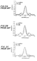
- FIGS.2B and 2C respectively show the distributions for the cases where the width L2 of the SiO 2 layer (phase shift part) 13 varies by ⁇ 0.05 ⁇ m over the wafer.
- the solid line indicates the distribution at a defocus of 0.000 ⁇ m
- the dashed line indicates the distribution at a defocus of 0.300 ⁇ m
- a fine dotted line indicates the distribution at a defocus of 0.600 ⁇ m
- the one-dot chain line indicate the distribution at a defocus of 0.900 ⁇ m
- the two-dot chain line indicates the distribution at a defocus of 1.200 ⁇ m.
- the wavelength ⁇ of the exposure light is 0.365 ⁇ m
- the numerical aperture (NA) of the exposure lens is 0.54
- the coherency factor ⁇ is 0.30.
- the resist layer on the wafer is exposed by the peaks appearing on both sides of the distribution, and more of the resist layer is developed when compared to the case shown in FIG.2A.
- the width of the opening in the resist layer after the developing is approximately the distance in the distribution at the light intensity of 0.3.
- the width of the opening in the resist layer is 0.35 ⁇ m which is slightly smaller than the width of 0.36 ⁇ m which is obtained in the case shown in FIG.2A.
- the width of the opening in the resist layer is 0.39 ⁇ m which is considerably greater than the 0.36 ⁇ m obtained in the case shown in FIG.2A. Therefore, it can be seen that the deviation of ⁇ 0.05 ⁇ m of the width L2 exceeds the tolerable deviation range.
- the side etching of the Cr layer 12 lacks stability, and the side etching rate is greatly dependent on the conditions of the preprocess carried out before the side etching and also the etching pattern or etching area. Particularly, the side etching rate varies from 0.03 ⁇ m/min to 0.07 ⁇ m/min, and under this variation range, an error of 0.05 ⁇ m appears on the wafer at 3 ⁇ . Therefore, as described above, it is extremely difficult to control the width L2 of the SiO 2 layer 13 to a desired value which is within a tolerable range when the side etching of the Cr layer 12 is required.
- phase shift optical mask used for exposing a pattern using an exposure light, comprising a substrate which is transparent with respect to the exposure light, a light blocking layer which is non-transparent with respect to the exposure light and is provided on the substrate, where the light blocking layer has an opening having a predetermined shape and size and being defined by a side wall of the light blocking layer, and a phase shift layer which is transparent with respect to the exposure light and is provided on the light blocking layer and the substrate which is exposed within the opening.
- the phase shift layer has a uniform thickness
- the light blocking layer has a predetermined thickness so that a phase of the exposure light transmitted through the phase shift layer provided on the side wall of the light blocking layer is shifted by approximately 180° relative to a phase of the exposure light transmitted through the phase shift layer provided on the substrate.
- the present divisional invention provides a phase shift optical mask for exposing a pattern on a wafer via an exposure lens using an exposure light, comprising: a substrate which is transparent with respect to the exposure light, a light-transmitting region on the substrate and having a width m(L + 0.2 ⁇ /NA), where m denotes the reducing projection magnification, L denotes the width of the opening actually developed on the wafer, ⁇ denotes the wavelength of the exposure light and NA denotes the numerical aperture of the exposing lens; a first phase-shift region which is transparent with respect to the exposure light and is provided to a width (m ⁇ /2NA)[1.1 - (NA/ ⁇ )(L + 0.2 ⁇ /NA)] around the periphery of the light-transmitting region; a first light-blocking region which is non-transparent with respect to the exposure light and is provided to a width 0.1m ⁇ /NA around the outside of the first phase-shift region; a second phase-shift region which is transparent with respect to the exposure light,
- the invention is also concerned with a corresponding method, which comprises the steps of:
- the phase shift optical mask includes a glass substrate 1, a light blocking layer 2, a first inorganic layer 3 and a second inorganic layer 4.
- a main light transmitting part A is surrounded by a phase shift part B.
- the first and second inorganic layers 3 and 4 are respectively made of an inorganic material, and the second inorganic layer 4 has a thickness T.
- the total thickness PS of the light-blocking layer 2 and the first inorganic layer 3 corresponds to a phase shift of approximately 180°.
- FIG.3B shows the amplitude and the phase characteristic of the light which is transmitted through the main light transmitting part A and the phase shift part B of the phase shift optical mask.
- a curve I indicates the light transmitted through the main light transmitting part A
- a curve II indicates the light transmitted through the phase shift part B.
- the phase of the light transmitted through the phase shift part B is shifted by 180° with respect to the phase of the light transmitted through the main light transmitting part A.
- FIG.3C shows the amplitude and the phase characteristic of the synthesized light in which the light transmitted through the main light transmitting part A and the light transmitted through the phase shift part B are superimposed.
- the curve III of this synthesized light is sharper than the curve I because, at the bottom of the curve III, the light transmitted through the main light transmitting part A is cancelled by the light which is transmitted through the phase shift part B and has an inverted phase with respect to the light transmitted through the main light transmitting part A.
- curve IV indicates the intensity of the transmitted light. This curve IV corresponds to the square of the amplitude indicated by the curve III shown in FIG.3C. The curve IV is very sharp because of the light transmitted through the phase shift part B. Hence, it may be seen from FIG.3D that the resulution is improved when carrying out the exposure.
- the light blocking layer 2 is formed on the entire surface of the glass substrate 1, and the first inorganic layer 3 is formed on the entire surface of the light blocking layer 2.
- the total thickness PS of the light blocking layer 2 and the first inorganic layer 3 is set so that the exposure light is shifted by 180° by the second inorganic layer 4 which is later formed.
- the thickness PS for realizing the 180° phase shift by use of the second inorganic layer 4 is calculated as follows. Since the propagation velocity of the exposure light is inversely proportional to the refractive index of the medium through which the exposure light propagates, the thickness of the medium should be set to ⁇ /2(n-1) when shifting the phase of the exposure light by 180° compared to the exposure light propagating through air, where n denotes the refractive index of the medium and ⁇ denotes the wavelength of the exposure light.
- the thickness PS can be realized using only the light blocking layer 2.
- problems are introduced due to a difference between coefficients of thermal expansion of the layers if the metal light blocking layer 2 is made thick.
- the metal light blocking layer 2 is thick, the etching of the metal light blocking layer 2 at the later stage becomes that much more difficult.
- an opening 5 for exposure is formed in the first organic layer 3 and the light blocking layer 2 by a photolithography technique.
- the width of this opening 5 is A+2T, where A denotes the width of the main light transmitting part A after completion and T denotes the thickness of the second inorganic layer 4 which is later formed.
- the width of the opening 5 is 2T wider than the width of the opening 14 of the conventional phase shift optical mask shown in FIG.1, thereby making it possible to accurately form the opening 5 with a satisfactory reproducibility using the normal photolithography technique.
- the second inorganic layer 4 is formed on the first inorganic layer 3 and the glass substrate 1 which is exposed within the opening 5, using chemical vapor deposition (CVD) or the like.
- the thickness of the second inorganic layer 4 which is formed by the CVD is uniform, and the thickness T of the second inorganic layer 4 deposited on the first inorganic layer 3 can be made the same as the width T of the second inorganic layer 4 which is deposited on the inner wall defining the opening 5.
- the depression of the stepped part which is formed at the surface of the second inorganic layer 4 is maintained the same as the total thickness PS of the light blocking layer 2 and the first inorganic layer 3.
- the depression functions as the main light transmitting part A, and the region of width T that is formed on the outer side of the depression on each side functions as the phase shift part B.
- the size of the completed main light transmitting part A can be controlled accurately using the width A+2T of the opening 5 as a reference, which opening 5 is formed by the normal photolithography technique.
- the phase shift optical mask 34 shown in FIG.4 includes a Cr light blocking layer 7 which is formed on a quartz glass substrate 6, a SiO 2 first inorganic layer 8 which is formed on the Cr light blocking layer 7, an opening 10 which is formed in the SiO 2 first inorganic layer 8 and the Cr light blocking layer 7, and a SiO 2 second inorganic layer 9 which is formed on the SiO 2 inorganic layer 8 and the quartz glass substrate 6 which is exposed within the opening 10.
- the SiO 2 second inorganic layer 9 is transparent with respect to the exposure light.
- a main light transmitting part A is surrounded by the phase shift part B.
- This optical mask according to Fig. 4 may be produced by a first embodiment of a method of producing the optical mask according to the parent invention, as follows. According to the method, the Cr layer 7 is formed on the quartz glass substrate 6 and the SiO 2 layer 8 is formed on the Cr layer 7,so that the total thickness of the Cr layer 7 and the SiO 2 layer 8 becomes 4700 ⁇ .
- the total thickness of the Cr layer 7 and the SiO 2 layer 8 is calculated as follows. That is, since the propagation velocity of the exposure light is inversely proportional to the refractive index of the medium through which the exposure light propagates, the thickness of the medium should be set to ⁇ /2(n-1) when shifting the phase of the exposure light by 180° compared to the exposure light propagating through air, where n denotes the refractive index of the medium and ⁇ denotes the wavelength of the exposure light.
- the total thickness of the Cr layer 7 and the SiO 2 layer 8 can be calculated from ⁇ /2(n-1) as 4737 ⁇ or approximately 4700 ⁇ .
- a resist layer (not shown) is formed on the entire surface of the SiO 2 layer 8, and a resist mask pattern having an opening is formed by a normal electron beam exposure technique.
- One side of this opening in the resist mask pattern has a length of 1.1 x m ⁇ m when the reducing projection magnification of a reducing projection type exposure apparatus used is m.
- the SiO 2 layer 8 and the Cr layer 8 are selectively removed via this opening in the resist mask pattern using a dry etching, thereby forming an opening 10.
- the SiO 2 layer 9 is deposited to a thickness of 1 ⁇ m on the entire surface of the SiO 2 layer 8 and the quartz glass substrate 6 which is exposed within the opening 10 using a CVD.
- the phase shift optical mask 34 which is produced by the above described processes has a square main light transmitting part A having a side of 0.7 x m ⁇ m, and a frame shaped phase shift part B having a width of 0.2 x m ⁇ m.
- the square opening in the resist mask pattern which is formed on the SiO 2 layer 8 has a side of 5.5 ⁇ m, and when the phase shift optical mask 34 is completed, the square main light transmitting part A has a side of 3.5 ⁇ m and the frame shaped phase shift part B has a width of 1 ⁇ m.
- a resist layer which is formed on a semiconductor surface is exposed by passing a g-ray having a wavelength of 4358 ⁇ from a mercury discharge lamp through an optical pattern of the phase shift optical mask 34 and projecting the transmitted g-ray on the resist layer with a size reduction to 1/5, for example.
- the NA of the exposure lens is 0.45.
- FIG.5 generally shows an exposure apparatus which is used for carrying out the method.
- the g-ray emitted from a mercury discharge lamp 31 irradiates the phase shift optical mask (or reticle) 34 via a condenser lens 32 and an iris 33, and the g-ray transmitted through the phase shift optical mask 34 is converged and irradiates a wafer 36 via a projection lens 35.
- the wafer 36 corresponds to the semiconductor surface referred above, and the resist layer which is exposed is formed on the wafer 36.
- the width T of the SiO 2 layer (phase shift part) 4 can be controlled accurately by controlling the deposition thickness of the SiO 2 layer 4.
- the deposition thickness of the SiO 2 layer 4 can be controlled within the range ⁇ 0.02 ⁇ m on the phase shift optical mask 34.
- this range is reduced to 1/5 because of the reduced production, and the error on the wafer 36 is of the order of ⁇ 0.004 ⁇ m at 3 ⁇ .
- This error of ⁇ 0.004 ⁇ m is considerably smaller than the error of ⁇ 0.05 ⁇ m which is introduced in the conventional case described above.
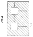
- FIG.6 shows a plan view of an actual pattern which is formed on the wafer 36 using the optical mask 34.
- the optical mask 34 is particularly suited for use in forming a fine aperture 340 of the pattern shown in FIG.6.
- the phase shift optical mask was developed to improve the resolution of the photolithography technique.
- the phase shift optical mask includes a first region for transmitting the exposure light as it is and a second region for inverting the phase of the exposure light, and the second region is formed adjacent to or in a vicinity of the first region.
- the widths of the first and second regions are determined by the wavelength of the exposure light and the NA of the exposure lens, and these first and second regions effectively utilize the light interference.
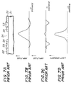
- FIG.7A shows another conventional phase shift optical mask including a glass substrate 21, a Cr light blocking layer 22 and a SiO 2 phase shift layer 23.
- the amplitude of the exposure light which is transmitted through a light transmitting region 24 of this phase shift optical mask is shown in FIG.7B, while the amplitude of the exposure light which is transmitted through the SiO 2 phase shift layer 23 is shown in FIG.7C.
- a positive direction indicates a positive phase and a negative direction indicates an inverted phase.
- the light intensity of the exposure light transmitted through the phase shift optical mask that is, the light intensity of the synthesized light, made up of the exposure light transmitted through the light transmitting region 24 and the exposure light transmitted through the SiO 2 phase shift layer 23, becomes as shown in FIG.7D. Therefore, it is possible to draw or expose an extremely thin line using this phase shift optical mask.
- FIG.8A shows a further conventional phase shift optical mask including a glass substrate 21, a Cr light blocking layer 25 and a SiO 2 phase shift layer 26.
- the amplitude of the exposure light which is transmitted through a light transmitting region 27 of this phase shift optical mask is shown in FIG.8B, while the amplitude of the exposure light which is transmitted through the SiO 2 phase shift layer 26 is shown in FIG.8C.
- a positive direction likewise indicates a positive phase and a negative direction indicates an inverted phase.
- the light intensity of the exposure light transmitted through the phase shift optical mask that is, the light intensity of the synthesized light,made up of the exposure light transmitted through the light transmitting region 27 and the exposure light transmitted through the SiO 2 phase shift layer 26, becomes as shown in FIG.8D. Therefore, it is possible to draw or expose an extremely thin line using this phase shift optical mask.
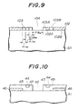
- a phase shift optical mask which combines the concepts of the first and second conventional phase shift optical masks shown in FIGS.7A and 8A has the structure shown in FIG.9.
- the phase shift optical mask shown in FIG.9 includes a glass substrate 101, a Cr light blocking layer 102 which includes first and second light blocking regions 102A and 102B, a SiO 2 phase shift layer 103 which includes first and second phase shift regions 103A and 103B, and a light transmitting region 104.
- the width of the light transmitting region 104 must be set to m x 0.6 ⁇ m
- the width of the first phase shift region 103A must be set to m x 0.25 ⁇ m
- the width of the first light blocking region 102A must be set to m x 0.1 ⁇ m
- the width of the second phase shift region 103B must be set to m x 0.1 ⁇ m, where m denotes the reducing projection magnification which is normally 5 or less.
- FIG.10 shows an essential part of the embodiment of the optical mask according to the present invention.
- the optical mask shown in FIG.10 includes a light transmitting substrate 41, a light transmitting region 42, a first phase shift layer 43, a first light blocking layer 44, a second phase shift layer 45, and a second light blocking layer 46.
- the light transmitting substrate 41 is made of quartz glass
- the first and second phase shift layers 43 and 45 are made of SiO 2
- the first and second light blocking layers 44 and 46 are made of Cr.
- the first phase shift layer 43 is provided on the outer side of the light transmitting region 42.
- the first light blocking layer 44 is provided on the outer side of the first phase shift layer 43.
- the second phase shift layer 45 is provided on the outer side of the first light blocking layer 44.
- the second light blocking layer 46 is provided on the outer side of the second phase shift layer 45.
- the light transmitting region 42 has a width of the order of m(L + 0.2 ⁇ /NA)
- the first phase shift layer 43 has a width of the order of (m ⁇ /2NA)[1.1 - (NA/ ⁇ )(L + 0.2 ⁇ /NA)]
- the first light blocking layer 44 has a width of the order of 0.1m ⁇ /NA, where m denotes the reducing projection magnification, L denotes the width of the actual opening which is formed on the wafer, ⁇ denotes the wavelength of the exposure light and NA denotes the numerical aperture of the exposure lens.
- FIG.11A shows the amplitude and a phase characteristic of light transmitted through the light transmitting region 42, the first phase shift layer (region) 43 and the second phase shift layer (region) 45 of the optical mask shown in FIG.10
- FIG.11B shows the light intensity of transmitted light in correspondence with FIG.11A.
- G denotes the amplitude of the light transmitted through the light transmitting region 42
- H denotes the amplitude of the light transmitted through the first phase shift layer 43
- I denotes the amplitude of the light transmitted through the second phase shift layer 45.
- the intensity of the light transmitted through the optical mask shown in FIG.10 as a whole is a synthesized light of G, H and I, as indicated by J in FIG.11B.
- the effective exposure width can be set to 0.4 ⁇ m, for example, thereby enabling a considerable improvement of the resolution when compared to the conventional phase shift optical masks.
- phase shift layer 47 which covers the light transmitting region 42, the first phase shift layer 43, the first light blocking layer 44 and the second phase shift layer 45.
- FIGS.12A to 12C a description will be given of an embodiment of the method of producing the optical mask according to the present example, by referring to FIGS.12A to 12C.
- the embodiment of the optical mask shown in FIG.10 is produced.
- FIGS.12A to 12C those parts which are the same as those corresponding parts in FIG.10 are designated by the same reference numerals, and a description thereof will be omitted.
- a Cr layer 46 is formed on the quartz glass substrate 41 to a thickness of 4700 ⁇ which corresponds to ⁇ /(2n - 2), where ⁇ denotes the wavelength of the exposure light and n denotes the refractive index of SiO 2 which is used as the phase shift material of this optical mask.
- An opening having a width of 7.5 ⁇ m is formed in the Cr layer 46 using a photolithography technique.
- a SiO 2 layer 45a is formed to a thickness of 5000 ⁇ . This SiO 2 layer 45a covers the Cr layer 46 and the surface of the quartz glass substrate 42 which is exposed within the opening.
- a Cr layer 44a is formed on the SiO 2 layer 45a to a thickness of 5000 ⁇ .
- the width of the side wall at the stepped part of the Cr layer 44a and the width of the side wall at the stepped part of the SiO 2 layer 45a both become 0.5 ⁇ m.
- a reactive etching using a gas mixture of carbon tetrafluoride (CF 4 ) and oxygen (O 2 ) as the reactive gas is carried out to etch back the Cr layer 44a so as to leave the first light blocking layer 44 at the side wall of the stepped part of the SiO 2 layer 45a as shown in FIG.12B.
- a SiO 2 layer 43a is thereafter formed on the surface of the structure shown in FIG.12B to a thickness of 1 ⁇ m, as shown in FIG.12C.
- the width of the side wall at the stepped part of this SiO 2 layer 43a is 1 ⁇ m.
- the SiO 2 layer 43a is etched back by a reactive etching using CF 4 as the reactive gas, the first phase shift layer 43 is left on the side wall at the stepped part of the first light blocking layer 44 as shown in FIG.10.
- the SiO 2 layer 45a which remains on the side wall part at the stepped part of the Cr layer (second light blocking layer) 46 forms the second phase shift layer 45.
- an opening is formed in the phase shift layers 43 and 45 so as to form the light transmitting region 42.
- the first phase shift layer 43 in this case has a double-layer structure made up of the original first phase shift layer 43 and the SiO 2 layer 43a
- the second phase shift layer 45 has a double-layer structure made up of the original second phase shift layer 45 and the SiO 2 layer 43a.
- the second embodiment of the method carries out an etch back process after forming a phase shift layer and a light blocking layer on a stepped surface, it is possible to form a phase shift layer and a light blocking layer having an extremely narrow width with a high accuracy. Therefore, it is possible to expose line patterns having a width of 0.4 ⁇ m or even less.
- the second embodiment of the optical mask shown in FIG.12C may be regarded as the optical mask shown in FIG.4 added with the phase shift layer 43 and the light blocking layer 44.
Landscapes
- Physics & Mathematics (AREA)
- General Physics & Mathematics (AREA)
- Preparing Plates And Mask In Photomechanical Process (AREA)
- Exposure And Positioning Against Photoresist Photosensitive Materials (AREA)
Applications Claiming Priority (5)
| Application Number | Priority Date | Filing Date | Title |
|---|---|---|---|
| JP2237110A JPH04118654A (ja) | 1990-09-10 | 1990-09-10 | 位相シフト光学マスクおよびその製造方法 |
| JP237110/90 | 1990-09-10 | ||
| JP21483/91 | 1991-01-23 | ||
| JP2148391A JP3125104B2 (ja) | 1991-01-23 | 1991-01-23 | 光学マスク及びその製造方法 |
| EP91308195A EP0475694B1 (de) | 1990-09-10 | 1991-09-06 | Optische Phasenmaske und Verfahren zur Herstellung |
Related Parent Applications (1)
| Application Number | Title | Priority Date | Filing Date |
|---|---|---|---|
| EP91308195A Division EP0475694B1 (de) | 1990-09-10 | 1991-09-06 | Optische Phasenmaske und Verfahren zur Herstellung |
Publications (2)
| Publication Number | Publication Date |
|---|---|
| EP0843217A2 true EP0843217A2 (de) | 1998-05-20 |
| EP0843217A3 EP0843217A3 (de) | 1998-12-16 |
Family
ID=26358550
Family Applications (2)
| Application Number | Title | Priority Date | Filing Date |
|---|---|---|---|
| EP91308195A Expired - Lifetime EP0475694B1 (de) | 1990-09-10 | 1991-09-06 | Optische Phasenmaske und Verfahren zur Herstellung |
| EP98101274A Withdrawn EP0843217A3 (de) | 1990-09-10 | 1991-09-06 | Optische Phasenmaske und Verfahren zur Herstellung |
Family Applications Before (1)
| Application Number | Title | Priority Date | Filing Date |
|---|---|---|---|
| EP91308195A Expired - Lifetime EP0475694B1 (de) | 1990-09-10 | 1991-09-06 | Optische Phasenmaske und Verfahren zur Herstellung |
Country Status (4)
| Country | Link |
|---|---|
| US (1) | US5424153A (de) |
| EP (2) | EP0475694B1 (de) |
| KR (1) | KR950014324B1 (de) |
| DE (1) | DE69131173T2 (de) |
Cited By (1)
| Publication number | Priority date | Publication date | Assignee | Title |
|---|---|---|---|---|
| WO2001065316A1 (en) * | 2000-03-03 | 2001-09-07 | Koninklijke Philips Electronics N.V. | Method of manufacturing a device by means of a mask and phase-shifting mask for use in said method |
Families Citing this family (17)
| Publication number | Priority date | Publication date | Assignee | Title |
|---|---|---|---|---|
| US5595844A (en) * | 1990-11-29 | 1997-01-21 | Kabushiki Kaisha Toshiba | Method of exposing light in a method of fabricating a reticle |
| JPH04269750A (ja) * | 1990-12-05 | 1992-09-25 | American Teleph & Telegr Co <Att> | 離隔特徴をフォトレジスト層に印刷する方法 |
| EP0524741A1 (de) * | 1991-07-12 | 1993-01-27 | Motorola, Inc. | Verfahren zur Erhöhung der Bildauflösung einer Maske für die Herstellung von Halbleiterschaltungen |
| JP3194155B2 (ja) * | 1992-01-31 | 2001-07-30 | キヤノン株式会社 | 半導体デバイスの製造方法及びそれを用いた投影露光装置 |
| JPH10512683A (ja) * | 1993-01-21 | 1998-12-02 | セマテック,インコーポレーテッド | 改善されたイメージングのために吸収/減衰性側壁を備えた移相マスク構造および吸収/減衰性側壁を備えたシフターを作る方法 |
| US5418095A (en) * | 1993-01-21 | 1995-05-23 | Sematech, Inc. | Method of fabricating phase shifters with absorbing/attenuating sidewalls using an additive process |
| US5411824A (en) * | 1993-01-21 | 1995-05-02 | Sematech, Inc. | Phase shifting mask structure with absorbing/attenuating sidewalls for improved imaging |
| WO1994017449A1 (en) * | 1993-01-21 | 1994-08-04 | Sematech, Inc. | Phase shifting mask structure with multilayer optical coating for improved transmission |
| US5470681A (en) * | 1993-12-23 | 1995-11-28 | International Business Machines Corporation | Phase shift mask using liquid phase oxide deposition |
| TW270219B (de) * | 1994-05-31 | 1996-02-11 | Advanced Micro Devices Inc | |
| US5717218A (en) * | 1994-12-28 | 1998-02-10 | International Business Machines Corporation | Focal plane phase-shifting lithography |
| KR100627210B1 (ko) * | 1995-08-04 | 2006-12-01 | 다이니폰 인사츠 가부시키가이샤 | 위상시프트마스크 |
| KR100213250B1 (ko) * | 1996-10-10 | 1999-08-02 | 윤종용 | 위상 쉬프트 마스크 및 그 제조방법 |
| US6251546B1 (en) * | 1999-09-16 | 2001-06-26 | Agere Systems Guardian Corp. | Method of fabricating devices using an attenuated phase-shifting mask and an attenuated phase-shifting mask |
| US20050100798A1 (en) * | 2003-10-15 | 2005-05-12 | Taiwan Semiconductor Manufacturing Company, Ltd. | Device and method for providing wavelength reduction with a photomask |
| US20060083997A1 (en) * | 2003-10-15 | 2006-04-20 | Taiwan Semiconductor Manufacturing Company, Ltd. | Photomask with wavelength reduction material and pellicle |
| KR20160127276A (ko) * | 2015-04-24 | 2016-11-03 | 삼성디스플레이 주식회사 | 표시 장치 |
Family Cites Families (6)
| Publication number | Priority date | Publication date | Assignee | Title |
|---|---|---|---|---|
| JP2865685B2 (ja) * | 1988-03-16 | 1999-03-08 | 株式会社日立製作所 | 半導体装置の製造方法 |
| JP2710967B2 (ja) * | 1988-11-22 | 1998-02-10 | 株式会社日立製作所 | 集積回路装置の製造方法 |
| JPH02211451A (ja) * | 1989-02-13 | 1990-08-22 | Toshiba Corp | 露光マスク,露光マスクの製造方法及びこれを用いた露光方法 |
| EP0653679B1 (de) * | 1989-04-28 | 2002-08-21 | Fujitsu Limited | Maske, Verfahren zur Herstellung der Maske und Verfahren zur Musterherstellung mit einer Maske |
| DE69125195T2 (de) * | 1990-01-12 | 1997-06-26 | Sony Corp | Phasenverschiebungsmaske und Verfahren zur Herstellung |
| JP2566048B2 (ja) * | 1990-04-19 | 1996-12-25 | シャープ株式会社 | 光露光用マスク及びその製造方法 |
-
1991
- 1991-09-06 DE DE69131173T patent/DE69131173T2/de not_active Expired - Fee Related
- 1991-09-06 EP EP91308195A patent/EP0475694B1/de not_active Expired - Lifetime
- 1991-09-06 EP EP98101274A patent/EP0843217A3/de not_active Withdrawn
- 1991-09-10 KR KR1019910015744A patent/KR950014324B1/ko not_active Expired - Fee Related
-
1993
- 1993-10-22 US US08/139,782 patent/US5424153A/en not_active Expired - Fee Related
Cited By (1)
| Publication number | Priority date | Publication date | Assignee | Title |
|---|---|---|---|---|
| WO2001065316A1 (en) * | 2000-03-03 | 2001-09-07 | Koninklijke Philips Electronics N.V. | Method of manufacturing a device by means of a mask and phase-shifting mask for use in said method |
Also Published As
| Publication number | Publication date |
|---|---|
| KR950014324B1 (ko) | 1995-11-24 |
| DE69131173T2 (de) | 1999-08-19 |
| EP0475694A3 (en) | 1992-09-16 |
| EP0475694A2 (de) | 1992-03-18 |
| DE69131173D1 (de) | 1999-06-02 |
| US5424153A (en) | 1995-06-13 |
| EP0843217A3 (de) | 1998-12-16 |
| EP0475694B1 (de) | 1999-04-28 |
Similar Documents
| Publication | Publication Date | Title |
|---|---|---|
| EP0475694B1 (de) | Optische Phasenmaske und Verfahren zur Herstellung | |
| EP0653679B1 (de) | Maske, Verfahren zur Herstellung der Maske und Verfahren zur Musterherstellung mit einer Maske | |
| US5234780A (en) | Exposure mask, method of manufacturing the same, and exposure method using the same | |
| JP3368947B2 (ja) | レティクル及びレティクル・ブランク | |
| US6306547B1 (en) | Photomask and manufacturing method thereof, and exposure method using the photomask | |
| US5429897A (en) | Attenuating type phase shifting mask and method of manufacturing thereof | |
| KR940007788B1 (ko) | 사진석판술용 마스크 및 그 제조방법 | |
| JPH04136854A (ja) | 半導体装置の製造方法 | |
| US5840447A (en) | Multi-phase photo mask using sub-wavelength structures | |
| EP1321820A1 (de) | Halbton-phasenverschiebungs-photomaske und rolling für die halbton-phasenverschiebungsphotomaske | |
| US6372392B1 (en) | Transparent optical device and fabrication method thereof | |
| US5248575A (en) | Photomask with phase shifter and method of fabricating semiconductor device by using the same | |
| US5698349A (en) | Sub-resolution phase shift mask | |
| EP1172692A2 (de) | Rohling für Phasenschiebermaske, Phasenschiebermaske und Verfahren zu deren Herstellung | |
| JPH0627636A (ja) | フォトマスク及びフォトマスクの製造方法及びエッチング方法及び露光方法 | |
| US5468576A (en) | Method for manufacturing exposure mask | |
| JP3007846B2 (ja) | マスク及びその製造方法並びにマスクを用いたパターン形成方法 | |
| JP3301557B2 (ja) | 位相シフトフォトマスクの製造方法 | |
| JP2652341B2 (ja) | 位相反転マスクの製造方法 | |
| US6348288B1 (en) | Resolution enhancement method for deep quarter micron technology | |
| JP3434309B2 (ja) | 位相シフトマスクの製造方法 | |
| JP3225673B2 (ja) | 位相シフト・マスクの製造方法 | |
| JPH0659432A (ja) | 露光用マスク及びこれを使用した露光方法 | |
| JPH07159971A (ja) | 光学マスクブランクと光学マスクおよびそれらの製造方法 | |
| KR0172235B1 (ko) | 반도체 소자의 미세패턴 제조방법 |
Legal Events
| Date | Code | Title | Description |
|---|---|---|---|
| PUAI | Public reference made under article 153(3) epc to a published international application that has entered the european phase |
Free format text: ORIGINAL CODE: 0009012 |
|
| AC | Divisional application: reference to earlier application |
Ref document number: 475694 Country of ref document: EP |
|
| AK | Designated contracting states |
Kind code of ref document: A2 Designated state(s): DE FR GB |
|
| PUAL | Search report despatched |
Free format text: ORIGINAL CODE: 0009013 |
|
| AK | Designated contracting states |
Kind code of ref document: A3 Designated state(s): DE FR GB |
|
| 17P | Request for examination filed |
Effective date: 19990510 |
|
| 17Q | First examination report despatched |
Effective date: 20030317 |
|
| STAA | Information on the status of an ep patent application or granted ep patent |
Free format text: STATUS: THE APPLICATION IS DEEMED TO BE WITHDRAWN |
|
| 18D | Application deemed to be withdrawn |
Effective date: 20030729 |