EP0437712B1 - Tandem-Cache-Speicher - Google Patents
Tandem-Cache-Speicher Download PDFInfo
- Publication number
- EP0437712B1 EP0437712B1 EP90122942A EP90122942A EP0437712B1 EP 0437712 B1 EP0437712 B1 EP 0437712B1 EP 90122942 A EP90122942 A EP 90122942A EP 90122942 A EP90122942 A EP 90122942A EP 0437712 B1 EP0437712 B1 EP 0437712B1
- Authority
- EP
- European Patent Office
- Prior art keywords
- cache
- information
- address
- output
- block
- Prior art date
- Legal status (The legal status is an assumption and is not a legal conclusion. Google has not performed a legal analysis and makes no representation as to the accuracy of the status listed.)
- Expired - Lifetime
Links
Images


Classifications
-
- G—PHYSICS
- G06—COMPUTING OR CALCULATING; COUNTING
- G06F—ELECTRIC DIGITAL DATA PROCESSING
- G06F9/00—Arrangements for program control, e.g. control units
- G06F9/06—Arrangements for program control, e.g. control units using stored programs, i.e. using an internal store of processing equipment to receive or retain programs
- G06F9/30—Arrangements for executing machine instructions, e.g. instruction decode
- G06F9/38—Concurrent instruction execution, e.g. pipeline or look ahead
- G06F9/3802—Instruction prefetching
- G06F9/3814—Implementation provisions of instruction buffers, e.g. prefetch buffer; banks
-
- G—PHYSICS
- G06—COMPUTING OR CALCULATING; COUNTING
- G06F—ELECTRIC DIGITAL DATA PROCESSING
- G06F12/00—Accessing, addressing or allocating within memory systems or architectures
- G06F12/02—Addressing or allocation; Relocation
- G06F12/08—Addressing or allocation; Relocation in hierarchically structured memory systems, e.g. virtual memory systems
- G06F12/0802—Addressing of a memory level in which the access to the desired data or data block requires associative addressing means, e.g. caches
- G06F12/0844—Multiple simultaneous or quasi-simultaneous cache accessing
- G06F12/0855—Overlapped cache accessing, e.g. pipeline
- G06F12/0859—Overlapped cache accessing, e.g. pipeline with reload from main memory
-
- G—PHYSICS
- G06—COMPUTING OR CALCULATING; COUNTING
- G06F—ELECTRIC DIGITAL DATA PROCESSING
- G06F12/00—Accessing, addressing or allocating within memory systems or architectures
- G06F12/02—Addressing or allocation; Relocation
- G06F12/08—Addressing or allocation; Relocation in hierarchically structured memory systems, e.g. virtual memory systems
- G06F12/0802—Addressing of a memory level in which the access to the desired data or data block requires associative addressing means, e.g. caches
- G06F12/0893—Caches characterised by their organisation or structure
- G06F12/0897—Caches characterised by their organisation or structure with two or more cache hierarchy levels
-
- G—PHYSICS
- G06—COMPUTING OR CALCULATING; COUNTING
- G06F—ELECTRIC DIGITAL DATA PROCESSING
- G06F9/00—Arrangements for program control, e.g. control units
- G06F9/06—Arrangements for program control, e.g. control units using stored programs, i.e. using an internal store of processing equipment to receive or retain programs
- G06F9/30—Arrangements for executing machine instructions, e.g. instruction decode
- G06F9/38—Concurrent instruction execution, e.g. pipeline or look ahead
- G06F9/3802—Instruction prefetching
-
- G—PHYSICS
- G06—COMPUTING OR CALCULATING; COUNTING
- G06F—ELECTRIC DIGITAL DATA PROCESSING
- G06F12/00—Accessing, addressing or allocating within memory systems or architectures
- G06F12/02—Addressing or allocation; Relocation
- G06F12/08—Addressing or allocation; Relocation in hierarchically structured memory systems, e.g. virtual memory systems
- G06F12/0802—Addressing of a memory level in which the access to the desired data or data block requires associative addressing means, e.g. caches
- G06F12/0862—Addressing of a memory level in which the access to the desired data or data block requires associative addressing means, e.g. caches with prefetch
Definitions
- the present invention relates to a tandem cache memory that is a cache memory comprising two cache memories which operate in parallel and support each other with the purpose of a fast servicing of information requests issued by a processor.
- buffer memories or “caches” are used, each coupled to a processor in the system.
- Each cache stores information most recently used by the related processor and provides such information on processor request, without need of access to the system bus.
- the caches of the first kind essentially comprise a "directory" or a list of block addresses and a memory storing the information blocks whose address is listed in the directory.
- the address of the block is the address field common to all addresses of the information items in the block.
- the information items in the same block are "contiguous" in the sense that their addresses differ in the least significant address bits only (their number depending on the block size) but the addresses of the several blocks are completely independent each from the other.
- the address is compared with the addresses stored in the cache directory.
- the requested information is stored in the cache and can be read out therefrom.
- the cache requests an information block containing the information to the working memory (through the system bus).
- the cache provides the requested information to the processing unit, with a delay or latency time corresponding to the time required to read the whole block or, in the best case (for very elaborated caches) to the time required to read the block portion preceding and containing the requested information.
- the cache cannot be further used by the processor and is "latent" for the whole time needed to load the whole block.
- the latency time may be further aggravated if the block loading must be preceded by a "replacement” operation, that is by the saving of the information stored in some zone of the cache in the working memory to give place in the cache to the new information block.
- the first kind caches offers the remarkable advantage that, as long as the requested information is contained in the cache, it may be supplied to the processor in a fast way and an unlimited number of times, independently of the order in which information items are requested.
- the cache of the second kind operate in a different way.
- a cache of this kind is for instance described in the European publication EP-A-0293720.
- the cache is loaded with the block containing the requested information and with the next following ordered block.
- the requested information is provided to the requesting processor as soon as available.
- the cache If the requested information is in a block already contained in the cache, but the next following block is not stored in the cache, the cache provides the requested information to the requesting processor without delay.
- the cache fetches the next following block from working memory and stores it.
- the prefetch unit and the microprocessor cache from an architectural standpoint woul be cascade connected or structured in a hierarchy as previosly mentioned: the first kind one would be connected between the microprocessor and the system bus, the second kind one would be connected between the system bus and the memory.
- a memory read request would be sent through the system bus to the memory system and, if the requested information is available in the second kind cache, it would be sent to the microprocessor and to the the first kind cache much faster than if it would be originally read from the memory into the prefetch unit.
- the sequential prefetching provided by the prefetching unit would not offer any substantive advantage, because memory accesses from the several processors (or units) are intermingled and sequentiality of addresses in memory accesses is generally lost.
- US-A-4,442,488 describes a cache memory system, which combines at some extent the functions of the first kind caches and the second kind caches by division of the cache in a plurality of regions: within each region information is prefetched in sequential order but the information stored in each region is address independent of thge one in the other regions.
- the arrangement is very complicated and very often results in a partial exploitation of the full size of the cache, because the regions must have a fixed size, whilst the the information sequences stored therein have a variable lenght, generally shorter than said fixed size.
- the cache memory cycle is splitted in two half cycles during which the cache is respectively read and written.
- the cache is inherently affected by a latency time, which however short is not negligible.
- the invention is defined in claim 1.
- tandem cache consisting in fact of two caches, coupled to operate in parallel and both located between a processor and the system bus.
- a first cache having a relatively high capacity is organized to store a plurality of independent blocks of information items.
- the second cache is organized to store a limited number of blocks, preferably four, of sequential information items.
- the first cache has its address input connected to the address input of the second cache and its information input/output connected to the information output of the second cache.
- the second cache performs subsequent read operations and fetches the block containing the requested information and the blocks having subsequent addresses in increasing order from working memory, loading them in suitable registers arranged to form a buffer.
- the requested information is forwarded to the requesting processor and at the same time the block containing it is loaded in the first cache.
- the information blocks having subsequent addresses are not stored in the first cache, with the advantage that the first cache remains free to respond to subsequent requests from the processor.
- the latency problem is therefore avoided and the first cache is not filled with information whose subsequent utilization is not certain.
- the second cache immediately provides it and at the same time transfers the block containing the requested information to the first cache.
- the requested information is available in the first cache, it is supplied to the requesting processor and the second cache remains inactive.
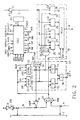
- Figure 1 shows in block diagram a data processing system including the tandem cache memory of the present invention.
- the system comprises a processor 1, including a memory management unit, the tandem cache memory 2, a working memory 3 and at least an input/output controller I/OC 4.
- a system bus 5 comprising a set of leads ABUS for transferring addresses, a set of leads DBUS for transferring data or instructions and a set of leads CBUS for transferring control signals, forms an intercommunication path for processor 1, working memory 3 and I/OC 4. Communication between processor 1 and bus 5, for having access to the working memory, occurs through the cache memory 2.
- the cache memory 2 is intended for storing instructions only and for fetching them from the working memory.
- Data read/write operations in the working memory 3, requested by processor 1, are performed through an interface unit 6, which, in turn, may include a data cache.
- tandem cache memory 2 may be implemented in a very simple way and described in an easily understandable manner.
- the cache memory 2 comprises a first cache 7, having a relatively high capacity, a second prefetching cache 8 and two sets of logical gates 9,10 for connection to the bus 5.
- gates 9 connect caches 7,8 to the address bus ABUS and gates 10 connect cache 8 to the data bus DBUS.
- the two caches 7,8 receives reading addresses, generated by processor 1, through a channel 11.
- cache 7 When a hit occurs in cache 7, cache 7 sends a signal HIT asserted to cache 8, through a lead 12.
- channel 14, data bus DBUS and working memory 3 have a 4 bytes parallelism.
- cache 7 sends signal HIT deasserted to cache 8.
- cache 8 sends the requested information to processor 1, through channel 14.
- control lead 15 In addition it controls cache 7, through control lead 15, so as to transfer the same information to cache 7, through channel 14.
- cache 8 Moreover if in cache 8 some space is available for storing a plurality of information blocks, cache 8 generates, on a bidirectional channel 16, the addresses of blocks next following those already stored in cache 8, requests access to the system bus (through control leads 171) and, once obtained it, controls a sequence of memory read operations, in burst mode, loading the received information in the available space.
- the information is received through gates 10 and a channel 17.
- the cache 8 operates as previously described to fetch, from the working memory, the block containing the requested instruction and a plurality of next following ordered blocks.
- Bidirectional gates 9, suitably controlled by cache 8 for receiving addresses from the system bus, enables the two caches 7,8 to systematically perform "bus watching" operations.
- cache 8 may detect, through channel 171, if a memory write operation is requested through the system bus.
- gates 9 are controlled so as to transfer to cache 7 and cache 8 (through channel 16) the write address present on bus 5.
- Both caches check if the referenced block i contained therein and in the affirmative they invalidate it.
- Figure 2 shows in block diagram and in greater detail a preferred embodiment of cache 8.
- Cache 8 comprises a logical sequencer SQC 18, which may be implemented as a finite states logical machine, an instruction buffer IPB 19, where a plurality of sequential blocks of instructions may be stored, a register IPBP 21 for storing the address of the first of the blocks which are actually stored in buffer 19, a counter register IPBL 22, an address comparing logic unit 23, a multiplexer 20 and a set of tristate gates 35.
- the comparison logic unit 23 comprises an AND gate 34, a subtractor 31 and two comparators 32,33.
- Subtractor 31 has the inputs connected to the output of registers 21 and 22.
- Comparator 32 has the inputs connected respectively to the output of multiplexer 20 and to the output of register 21.
- Comparator 32 output is connected to a first input of AND gate 34.
- Comparator 33 has the inputs connected respectively to the output of multiplexer 20 and to the output of counter register 22. Its output is connected to a second input of AND gate 34.
- Buffer 19 comprises four register 24,25,26,27, each having 32 bits and the inputs connected to channel 17 (which in turn is connected to data bus of system bus 5, through gates 10), a decoder 30 and a multiplexer 28.
- each register is connected to one input of the four input multiplexer 28.
- the output of multiplexer 28 is connected to channel 14.
- Multiplexer 28 is controlled by a selection code SC consisting in the two least significant bits in output from multiplexer 20.
- Code SC enables, in mutually exclusive way, one of the inputs to be connected to the output.
- the output of multiplexer 28 is enabled by a signal EN1, generated by sequencer 18.
- Decoder 30 has the input connected to the output of counter register 22 and receives the least significant bits of the register 22 output.
- Decoder 30 outputs, in mutually exclusive way, one of four selection signals SL1,SL2,SL3,SL4, each enabling the loading of one of the four registers 24,25,26,27.
- Loading is controlled by a signal LD generated by sequencer 18.
- Multiplexer 20 has a first input set connected to channel 11 and a second input set connected to channel 16.
- a signal BW, generated by sequencer 18, enables multiplexer 20 to transfer at its output the information present on channel 16 when "bus watching" detects write operations occurring on the system bus.
- the output of multiplexer 20 is connected to the input of the two registers 21,22, besides being connected to an input of comparators 32,33.
- Registers 21,22 are respectively controlled by parallel load signals LD1,LD2 and by an initialization reset signal RST.
- Register 22 is further controlled by an incrementing control signal INCR.
- the output of counter register 22 is connected to channel 16 through gates 35.
- Gates 35 are normally enabled to transfer addresses to channel 16 by signal NBW (BW negated).
- the addresses present on channel 11 and 16, as well as those at the output of registers 21,22 are block addresses and do not comprise the two least significant address bits which reference a "byte" within the information block.
- the two least significant bits of the block address at the output of multiplexer 20, form the selection code SC and the two least significant bits in output from register 22, and input to decoder 30, form a selection code for writing in one of registers 24,25,26,27.
- Subtractor 31 subtracts the contents of register 21 to the contents of register 22 and signals to sequencer 18, by a three bits code DIF what is the difference among the two contents.
- Sequencer 18 receives signal HIT from cache 7 and exchanges control signals with the system bus 5. These signals are not detailed because they clearly depend on the system bus protocol, being possible to select any one among several of the standard or non standard protocols known in the art.
- Sequencer 18 further receives signal HIT1 from gate 34 and a periodic clock signal CK from an oscillator 18A.
- Fig.3 and Fig.4 clarify the architecture of sequencer 18 as a finite state machine operating in accordance with predetermined logical flows and enlighten the operation of cache 8.
- Cache 8 normally inactive, is triggered by two external events: HIT deasserted by cache 7 joint with signals generated by processor 1, such as for instance AS, an address validation signal, and FCO, a signal qualifying the address as an instruction address, or by a write command SBW on bus 5, coupled with an address validation signal SBAS on system bus.
- processor 1 such as for instance AS, an address validation signal, and FCO
- a signal qualifying the address as an instruction address or by a write command SBW on bus 5, coupled with an address validation signal SBAS on system bus.
- the operations performed in the two cases are respectively shown in Fig.3 and Fig.4.
- cache 8 steps from an initial state IDLE (block 100) to a first active state 101 owing to external signals AS,FCO,NHIT.
- sequencer 18 checks if signal HIT1 is asserted or not.
- HIT1 is deasserted, this means that the address received on channel 11 through multiplexer 20 is not greater than or equal to the one stored in register 21, nor it is lesser than the one stored in register 22.
- This condition is for instance the one which occurs after an initialization which resets registers 21 and 22.
- the sequencer 18 loads the address present on channel 11 in registers 21 and 22 by means of commands LD1,LD2.
- the code DIF generated by subtractor 31 is, in this example, 000 and signals that the address stored in the two registers 21,22 differs for an amount zero.
- the sequencer 18 further provides to request access to the system bus 5, by setting a suitable flip flop indicating that a bus request BRQ is pending (block 102) and steps to a bus request and arbitration state 103, waiting to receive access.
- sequencer 18 exits from state 103 and steps to a state 104 which will be considered in the following.
- sequencer 18 steps in a state 105 and controls a working memory read operation, in burst mode, by asserting a signal SBRBURST, a code NBURST indicating the number of blocks to be read (in the example NBURST is the complement to 4 of code DIF) and by resetting the pending request indicator flip flop (signal RSBRQ).
- the gates 9 are enabled towards the system bus by a signal EN2 and gates 35 are enabled by signal NBW, so that the address stored in register 22 is transferred over the system bus 5.
- the address so transferred coincide with the block address received through channel 11.
- Cache 8 is preset to receive the requested information by signal EN which enables gates 10.
- the cache 8 After a certain time interval, the cache 8 receives a first information block, accompanied by a validation signal DVAL.
- the arbitrator 18 On receipt of such signal, the arbitrator 18 generates signal LD and loads the information block in the register, among registers 24,25,26, 27, which is selected by code SC.
- register 22 selects another register, among registers 24,25,26,27, as destination of a new information block when it will be received.
- the comparing unit 23 asserts HIT1.
- the sequencer 18 generates signal EN1 enabling multiplexer 28 to transfer the requested information block on channel 14 accompanied by a validation signal DTACK, which is sent through a lead 15 to both processor 1 and the cache 7 (Fig. 1).
- the block is received by the requesting processor 1 (which deasserts AS) and at the same time is loaded in cache 7, for possible subsequent use.
- Sequencer 18 does not limit itself to fetch an instruction block, but checks if the output of subtractor 31 indicates a difference equal to four, say the buffer capacity.
- the sequencer remains in state 103 and reenters in the flow already described at node 107, thus repeating the buffer 19 loading operation and counter 22 incrementation until DIF code indicates a value equal to 4.
- multiplexer 28 is disabled if signal AS is deasserted, that is if processor 1 does not need a new instruction contained in one of the subsequent blocks, stored in buffer 19.
- processor 1 and cache 7 receive the block containing the requested instruction as soon as it becomes available, without waiting for completion of the burst mode read operation.
- sequencer 18 steps to state 101, but being the signal HIT1 asserted, sequencer 18 asserts EN1 and DTACK and the requested block is immediately transferred to processor 1 and to cache 7.
- the selection of the buffer 19 register storing the block is performed by the address present on channel 11 and transferred through multiplexer 20 to the selection input of multiplexer 28.
- Sequencer 18 further asserts signal LD1 and loads the address at the output of multiplexer 20 in register 21.
- sequencer 18 checks if due to such operation the code DIF in output from subtractor 31 indicates a difference lesser than or equal to two (block 110).
- sequencer 18 steps from state 101 to state 103.
- the blocks are loaded in buffer 19.
- cache 7 provides the instruction and cache 8 remains inactive.
- cache 7 and cache 8 must check that the write operation on the system bus does not modify some information in a block which may be contained either in cache 7 or cache 8 or both.
- sequencer 18 steps to state 104, either from state 100 or from state 103 (Fig.3).
- sequencer 18 When in state 104, sequencer 18 asserts signal BW which controls multiplexer 20 and inhibits gates 35 so that the comparing unit 23 checks if the address on system bus is related to a block stored in buffer 19.
- sequencer 18 If signal HIT1 becomes asserted, sequencer 18 generates reset signals (RSIPBL,RSIPBP) which are directed to register 21,22 (signal RS of fig. 2) and steps to IDLE state 100.
- reset signals RSIPBL,RSIPBP
- sequencer 18 steps immediately to state 101 if a concurrent processor request has arised and signals AS,FCO,NHIT are pending (Fig. 3).
- sequencer 18 checks the pending request status BRQ, and if this condition is true, on the occurrence of the condition BGRANT, steps to state 105 of Fig.3.
- tandem cache memory specifically devoted to store instructions
- a cache such as cache 7 may be intended for storing both instructions and data
- a cache such 8 is intended for storing instructions only.
- tandem cache memory in which a cache for independent blocks of data and instructions is coupled to a pair of caches buffering sequential blocks, each of the caches of the pair being functionally equivalent to the cache 8 already described but intended for storing blocks of instructions and data blocks respectively.
Landscapes
- Engineering & Computer Science (AREA)
- Theoretical Computer Science (AREA)
- Software Systems (AREA)
- Physics & Mathematics (AREA)
- General Engineering & Computer Science (AREA)
- General Physics & Mathematics (AREA)
- Memory System Of A Hierarchy Structure (AREA)
Claims (3)
- Cache-Speichersystem (2) mit folgenden Merkmalen:einem ersten Cache (7) zum Speichern von Informationsblöcken, der einen Adresseneingang (11), einen Informationen-Eingang/Ausgang (14) und einen Signal-Ausgang (12) zum Signalisieren mit einem aktivierten bzw. deaktivierten Signal HIT aufweist, wenn Informationen, auf die durch eine Adresse verwiesen wird, die an dem Adresseneingang (11) empfangen wird, in dem ersten Cache gespeichert sind oder nicht, wobei der erste Cache (7) die Informationen, auf die verwiesen wird, an dem Informationen-Eingang/Ausgang (14) bei einer Aktivierung des Signals HIT ausgibt;einem zweiten Cache (8) zum Speichern von Informationsblöcken, auf die von aufeinanderfolgenden geordneten Adressen verwiesen wird, der einen Adresseneingang (11), der mit dem Adresseneingang (11) des ersten Cache (7) verbunden ist, einen Adressenausgang (16), einen Informationeneingang (17), einen Informationenausgang (14), der mit dem Informationen-Eingang/Ausgang (14) des ersten Cache (7) verbunden ist, und einen Eingang (12) zum Empfangen des Signals HIT von dem ersten Cache (7) aufweist;wobei der zweite Cache (8) eine Logikeinrichtung (18, 21, 22, 23), die durch das deaktivierte Signal HIT getriggert wird, zum Überprüfen aufweist, ob Informationen, auf die von einer an dem Adresseneingang (11) empfangenen Adresse verwiesen wird, in dem zweiten Cache (8) gespeichert oder nicht gespeichert sind;wobei, wenn solche Informationen nicht gespeichert sind, die Logikeinrichtung (18) zu einem Arbeitsspeicher (3) anfordert und eine Mehrzahl von Informationsblöcken mit aufeinanderfolgenden Adressen ansteigender Reihenfolge in den zweiten Cache (8) lädt, wobei die kleinere der aufeinanderfolgenden Adressen auf einen ersten Block verweist, der Informationen enthält, auf die von der Adresse verwiesen wird, die an dem Adresseneingang (11) empfangen wird, wobei die Logikeinrichtung (18) den ersten Block zu dem Informationenausgang (14) überträgt und den ersten Cache (7) anweist, um den ersten Block zu speichern, sobald derselbe von dem Arbeitsspeicher (3) empfangen ist, und zwar ohne darauf zu warten, die Mehrzahl von Informationsblöcken vollständig empfangen zu haben,wobei, wenn solche Informationen gespeichert sind, die Logikeinrichtung (18) den Informationenausgang (14) freigibt, um einen Informationenblock auszugeben, der die Informationen enthält, auf die von der Adresse, die an dem Adresseneingang (11) empfangen wird, verwiesen wird, und den ersten Cache (7) anweist, um den ausgegebenen Informationenblock zu speichern, und wobei die Logikeinrichtung (18, 23) ferner überprüft, ob sich die Adresse, die auf den ausgegebenen Block verweist, von der höheren der Adressen der Blöcke, die in dem zweiten Cache gespeichert sind, um weniger als einen vorbestimmten Betrag unterscheidet, und, wenn dies zutrifft, zu dem Arbeitsspeicher (3) anfordert und in den zweiten Cache (8) eine Mehrzahl von Informationsblöcken lädt, welche geordnete Adressen haben, die der höheren Adresse als nächstes folgen.
- Cache-Speichersystem gemäß Anspruch 1, bei dem der zweite Cache (8) eine Mehrzahl von Registern (24, 25, 26, 27) aufweist, wobei jedes zum Speichern eines Informationsblocks vorhanden ist, wobei die Logikeinrichtung (18, 21, 22, 23) folgende Merkmale aufweist:ein erstes Register (21) zum Speichern der Adresse eines Blocks, der in dem zweiten Block gespeichert ist, der die kleinere unter den Adressen der Blöcke, die in dem zweiten Cache (8) gespeichert sind, aufweist;ein zweites Register (22) zum Speichern der Adresse eines Blocks, der als nächstes der höchsten der Adressen der Blöcke, die in dem zweiten Cache (8) gespeichert sind, folgt; undeine Vergleichseinrichtung (23) zum Überprüfen, ob eine an dem Adresseneingang (11) empfangene Adresse höher oder gleich der in dem ersten Register (21) gespeicherten Adresse und kleiner als die in dem zweiten Register (22) gespeicherte Adresse ist, und wobei, wenn dies zutrifft, die Vergleichseinrichtung (23) ein aktiviertes Signal HIT1 erzeugt, wobei die Logikeinrichtung (18) beim Auftreten des aktivierten Signals HIT1 eines der Mehrzahl von Registern (24, 25, 26, 27) freigibt, um einen in demselben gespeicherten Informationsblock auszugeben, wobei das eine Register durch ein Feld der Adresse, die an dem Adresseneingang (11) empfangen wird, ausgewählt wird.
- Cache-Speichersystem gemäß Anspruch 1, bei dem der zweite Cache (8) einen Puffer (19) aufweist, der gleichzeitig gelesen und beschrieben werden kann.
Applications Claiming Priority (2)
| Application Number | Priority Date | Filing Date | Title |
|---|---|---|---|
| IT01909190A IT1238313B (it) | 1990-01-18 | 1990-01-18 | Memoria tampone in tandem |
| IT1909190 | 1990-01-18 |
Publications (3)
| Publication Number | Publication Date |
|---|---|
| EP0437712A2 EP0437712A2 (de) | 1991-07-24 |
| EP0437712A3 EP0437712A3 (en) | 1991-11-13 |
| EP0437712B1 true EP0437712B1 (de) | 1997-04-02 |
Family
ID=11154455
Family Applications (1)
| Application Number | Title | Priority Date | Filing Date |
|---|---|---|---|
| EP90122942A Expired - Lifetime EP0437712B1 (de) | 1990-01-18 | 1990-11-30 | Tandem-Cache-Speicher |
Country Status (3)
| Country | Link |
|---|---|
| EP (1) | EP0437712B1 (de) |
| DE (1) | DE69030368T2 (de) |
| IT (1) | IT1238313B (de) |
Families Citing this family (6)
| Publication number | Priority date | Publication date | Assignee | Title |
|---|---|---|---|---|
| DE69327981T2 (de) * | 1993-01-21 | 2000-10-05 | Advanced Micro Devices, Inc. | Kombinierte Speicheranordnung mit einem Vorausholungspuffer und einem Cachespeicher und Verfahren zur Befehlenversorgung für eine Prozessoreinheit, das diese Anordnung benutzt. |
| US5603004A (en) * | 1994-02-14 | 1997-02-11 | Hewlett-Packard Company | Method for decreasing time penalty resulting from a cache miss in a multi-level cache system |
| FR2755523B1 (fr) * | 1996-11-05 | 1998-12-04 | Bull Sa | Circuit electrique pour echanger des donnees entre un microprocesseur et une memoire et calculateur comprenant un tel circuit |
| GB2401967B (en) * | 1999-12-30 | 2005-01-05 | Intel Corp | Dual cache system |
| US6829680B1 (en) | 2000-01-05 | 2004-12-07 | Sun Microsystems, Inc. | Method for employing a page prefetch cache for database applications |
| AU2472601A (en) * | 2000-01-05 | 2001-07-16 | Sun Microsystems, Inc. | A method for employing a page prefetch cache for database applications |
Family Cites Families (3)
| Publication number | Priority date | Publication date | Assignee | Title |
|---|---|---|---|---|
| US4442488A (en) * | 1980-05-05 | 1984-04-10 | Floating Point Systems, Inc. | Instruction cache memory system |
| JPS6154547A (ja) * | 1984-08-24 | 1986-03-18 | インタ−ナショナル ビジネス マシ−ンズ コ−ポレ−ション | 3レベルの階層メモリを備えたデ−タ処理システム |
| IT1215539B (it) * | 1987-06-03 | 1990-02-14 | Honeywell Inf Systems | Memoria tampone trasparente. |
-
1990
- 1990-01-18 IT IT01909190A patent/IT1238313B/it active IP Right Grant
- 1990-11-30 DE DE69030368T patent/DE69030368T2/de not_active Expired - Fee Related
- 1990-11-30 EP EP90122942A patent/EP0437712B1/de not_active Expired - Lifetime
Also Published As
| Publication number | Publication date |
|---|---|
| DE69030368D1 (de) | 1997-05-07 |
| IT9019091A1 (it) | 1991-07-19 |
| EP0437712A3 (en) | 1991-11-13 |
| EP0437712A2 (de) | 1991-07-24 |
| DE69030368T2 (de) | 1997-07-17 |
| IT1238313B (it) | 1993-07-12 |
Similar Documents
| Publication | Publication Date | Title |
|---|---|---|
| CA1322058C (en) | Multi-processor computer systems having shared memory and private cache memories | |
| US6272579B1 (en) | Microprocessor architecture capable of supporting multiple heterogeneous processors | |
| US5524235A (en) | System for arbitrating access to memory with dynamic priority assignment | |
| US4733346A (en) | Data processor with multiple register blocks | |
| US5375223A (en) | Single register arbiter circuit | |
| EP0604139B1 (de) | Rechnersystem mit einem Vorausholungscachespeicher | |
| KR100194253B1 (ko) | 메시 데이터 코히어런시 프로토콜 이용 방법 및 멀티프로세서 시스템 | |
| US5463753A (en) | Method and apparatus for reducing non-snoop window of a cache controller by delaying host bus grant signal to the cache controller | |
| US5526508A (en) | Cache line replacing system for simultaneously storing data into read and write buffers having multiplexer which controls by counter value for bypassing read buffer | |
| US6134633A (en) | Prefetch management in cache memory | |
| US4586133A (en) | Multilevel controller for a cache memory interface in a multiprocessing system | |
| US4872138A (en) | Transparent cache memory | |
| US5313591A (en) | Computer bus arbitration for N processors requiring only N unidirectional signal leads | |
| US6332179B1 (en) | Allocation for back-to-back misses in a directory based cache | |
| US5659707A (en) | Transfer labeling mechanism for multiple outstanding read requests on a split transaction bus | |
| EP0283891B1 (de) | Cachespeicher mit Treffervorhersagelogik | |
| US6449698B1 (en) | Method and system for bypass prefetch data path | |
| EP0531003A1 (de) | Datenverarbeitung mit Prioritätssteuerungen für Reservierung eines bidirektionellen Datenbusses | |
| KR100322223B1 (ko) | 대기행렬및스누프테이블을갖는메모리제어기 | |
| EP0437712B1 (de) | Tandem-Cache-Speicher | |
| JP2000242556A (ja) | 仮想インデックス仮想タグデータキャッシュ用に最適化されたハードウエアクリーニング機能 | |
| KR100282118B1 (ko) | 하이스루풋단일포트다중갱신유니트태그제어기 | |
| US6862646B2 (en) | Method and apparatus for eliminating the software generated ready-signal to hardware devices that are not part of the memory coherency domain | |
| US5361368A (en) | Cross interrogate synchronization mechanism including logic means and delay register | |
| KR100457478B1 (ko) | 메모리액세스방법및데이터처리시스템 |
Legal Events
| Date | Code | Title | Description |
|---|---|---|---|
| PUAI | Public reference made under article 153(3) epc to a published international application that has entered the european phase |
Free format text: ORIGINAL CODE: 0009012 |
|
| AK | Designated contracting states |
Kind code of ref document: A2 Designated state(s): DE FR GB |
|
| PUAL | Search report despatched |
Free format text: ORIGINAL CODE: 0009013 |
|
| AK | Designated contracting states |
Kind code of ref document: A3 Designated state(s): DE FR GB |
|
| 17P | Request for examination filed |
Effective date: 19920122 |
|
| 17Q | First examination report despatched |
Effective date: 19950726 |
|
| GRAG | Despatch of communication of intention to grant |
Free format text: ORIGINAL CODE: EPIDOS AGRA |
|
| GRAH | Despatch of communication of intention to grant a patent |
Free format text: ORIGINAL CODE: EPIDOS IGRA |
|
| GRAH | Despatch of communication of intention to grant a patent |
Free format text: ORIGINAL CODE: EPIDOS IGRA |
|
| GRAA | (expected) grant |
Free format text: ORIGINAL CODE: 0009210 |
|
| AK | Designated contracting states |
Kind code of ref document: B1 Designated state(s): DE FR GB |
|
| REF | Corresponds to: |
Ref document number: 69030368 Country of ref document: DE Date of ref document: 19970507 |
|
| ET | Fr: translation filed | ||
| PLBE | No opposition filed within time limit |
Free format text: ORIGINAL CODE: 0009261 |
|
| STAA | Information on the status of an ep patent application or granted ep patent |
Free format text: STATUS: NO OPPOSITION FILED WITHIN TIME LIMIT |
|
| 26N | No opposition filed | ||
| REG | Reference to a national code |
Ref country code: GB Ref legal event code: IF02 |
|
| PGFP | Annual fee paid to national office [announced via postgrant information from national office to epo] |
Ref country code: DE Payment date: 20041026 Year of fee payment: 15 Ref country code: GB Payment date: 20041026 Year of fee payment: 15 |
|
| PG25 | Lapsed in a contracting state [announced via postgrant information from national office to epo] |
Ref country code: GB Free format text: LAPSE BECAUSE OF NON-PAYMENT OF DUE FEES Effective date: 20051130 |
|
| PG25 | Lapsed in a contracting state [announced via postgrant information from national office to epo] |
Ref country code: DE Free format text: LAPSE BECAUSE OF NON-PAYMENT OF DUE FEES Effective date: 20060601 |
|
| GBPC | Gb: european patent ceased through non-payment of renewal fee |
Effective date: 20051130 |
|
| PGFP | Annual fee paid to national office [announced via postgrant information from national office to epo] |
Ref country code: FR Payment date: 20071129 Year of fee payment: 18 |
|
| REG | Reference to a national code |
Ref country code: FR Ref legal event code: TP Ref country code: FR Ref legal event code: CD |
|
| REG | Reference to a national code |
Ref country code: FR Ref legal event code: TP |
|
| REG | Reference to a national code |
Ref country code: FR Ref legal event code: ST Effective date: 20090731 |
|
| PG25 | Lapsed in a contracting state [announced via postgrant information from national office to epo] |
Ref country code: FR Free format text: LAPSE BECAUSE OF NON-PAYMENT OF DUE FEES Effective date: 20081130 |