EP0438309A2 - Interpolierender Frequenzsynthetisierer mit Phasenregelkeis - Google Patents
Interpolierender Frequenzsynthetisierer mit Phasenregelkeis Download PDFInfo
- Publication number
- EP0438309A2 EP0438309A2 EP91300361A EP91300361A EP0438309A2 EP 0438309 A2 EP0438309 A2 EP 0438309A2 EP 91300361 A EP91300361 A EP 91300361A EP 91300361 A EP91300361 A EP 91300361A EP 0438309 A2 EP0438309 A2 EP 0438309A2
- Authority
- EP
- European Patent Office
- Prior art keywords
- pulse
- delay
- frequency
- pulses
- phase detector
- Prior art date
- Legal status (The legal status is an assumption and is not a legal conclusion. Google has not performed a legal analysis and makes no representation as to the accuracy of the status listed.)
- Granted
Links
- 230000002250 progressing effect Effects 0.000 claims 1
- 230000001360 synchronised effect Effects 0.000 claims 1
- 238000001208 nuclear magnetic resonance pulse sequence Methods 0.000 description 10
- 230000001934 delay Effects 0.000 description 5
- 230000003111 delayed effect Effects 0.000 description 3
- 238000010586 diagram Methods 0.000 description 2
- 238000000034 method Methods 0.000 description 2
- 230000000630 rising effect Effects 0.000 description 2
- 230000015572 biosynthetic process Effects 0.000 description 1
- 125000004122 cyclic group Chemical group 0.000 description 1
- 230000000694 effects Effects 0.000 description 1
- 238000001914 filtration Methods 0.000 description 1
- 230000007774 longterm Effects 0.000 description 1
- 238000004519 manufacturing process Methods 0.000 description 1
- 230000000087 stabilizing effect Effects 0.000 description 1
- 238000003786 synthesis reaction Methods 0.000 description 1
- 230000002194 synthesizing effect Effects 0.000 description 1
Images

Classifications
-
- H—ELECTRICITY
- H03—ELECTRONIC CIRCUITRY
- H03L—AUTOMATIC CONTROL, STARTING, SYNCHRONISATION OR STABILISATION OF GENERATORS OF ELECTRONIC OSCILLATIONS OR PULSES
- H03L7/00—Automatic control of frequency or phase; Synchronisation
- H03L7/06—Automatic control of frequency or phase; Synchronisation using a reference signal applied to a frequency- or phase-locked loop
- H03L7/16—Indirect frequency synthesis, i.e. generating a desired one of a number of predetermined frequencies using a frequency- or phase-locked loop
- H03L7/18—Indirect frequency synthesis, i.e. generating a desired one of a number of predetermined frequencies using a frequency- or phase-locked loop using a frequency divider or counter in the loop
- H03L7/197—Indirect frequency synthesis, i.e. generating a desired one of a number of predetermined frequencies using a frequency- or phase-locked loop using a frequency divider or counter in the loop a time difference being used for locking the loop, the counter counting between numbers which are variable in time or the frequency divider dividing by a factor variable in time, e.g. for obtaining fractional frequency division
- H03L7/1974—Indirect frequency synthesis, i.e. generating a desired one of a number of predetermined frequencies using a frequency- or phase-locked loop using a frequency divider or counter in the loop a time difference being used for locking the loop, the counter counting between numbers which are variable in time or the frequency divider dividing by a factor variable in time, e.g. for obtaining fractional frequency division for fractional frequency division
Definitions
- the present invention concerns an interpolating digital frequency synthesizer based on phase locking, with which such frequencies positioned between frequencies defined by integer divisors can be produced.
- the divided basic frequency f o /M determines the frequency of the pulses from the phase detector and the so-called frequency raster, this being the smallest programmable frequency interval.
- the pulses of the first input signal applied to the phase detector are each separately lengthened by a time corresponding to a given integer number k1 of pulse lengths of the pulses formed in the member, and in the other second member the pulses of the second input signal applied to the phase detector, are each separately lengthened by a time corresponding to a given integer number k2 of pulse lengths of the pulses formed in the member.
- the reference frequency is multiplied by a coefficient L, whereby a pulse sequence of frequency f o ⁇ L is obtained.
- the reference frequency is multiplied with coefficient L + ⁇ L, whereby a pulse sequence of frequency f ⁇ (L + ⁇ L) is obtained, and the pulses divided from the VCO frequency coming to the phase detector are lengthened by a time corresponding to k2 pulses of said frequency, whereby the pulse length of the pulse sequence going to the phase detector from the direction of the VCO will be
- the fractions of the frequencies are produced by lengthening the whole pulses coming to the phase detector by partial fractions k1 and k2. Since then the pulse edges no longer coincide in time with the edges of the f o or VCO frequency pulses, the coefficients k1 and k2 have to be updated cyclically for each pulse. The pulses then become symmetrical and the VCO frequency remains an unmodulated point frequency.
- the frequency of the pulses entering into the phase detector is no longer constant, f o /M, but it varies in the range f o /M+1 to f o /M, that is, little enough not to have any effect on the operation of the loop filter.
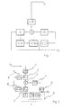
- the synthesizer of Fig. 1 is already described in the general section of the disclosure.
- the preferred embodiment of Fig. 2 deviates from the one presented above in that it includes blocks 2,9 and 7,8.
- the multiplication is accomplished in that e.g. the speed of the delay chain of length L in Fig. 1 is adjusted to be such that the edge of the f o frequency pulse needs exactly the time 1/f o to traverse the entire chain.
- the pulse delay consistent with the multiplied frequency is then obtained by selecting for the output of the delay register the output of the delay element representing the desired delay.
- the multiplication may also be carried out by forming within the circuit by VCO technique actual frequencies which on division by L and L+ ⁇ L will form the reference frequency f o , although this would be a poor design in view of circuit structures as well as power consumption.
- the delay chain of Fig. 3 consists of L or L+ ⁇ L identical voltage-controlled delay elements 41, the phase of the pulse that has passed therethrough is compared in the phase detector 42 with that of the pulse that is fed in. The delay is adjusted with the delay member 43 to be such that the phases of the pulse that has passed through the chain and of that fed into it are the same or, if desired, inverted.
- the delay of each delay element becomes set at the 1/L or 1/(L+ ⁇ L) fraction of the delay of the f o frequency pulse, and the desired multiple of this 1/L fraction delay is obtained by selecting for output 44, with switches S1 to S n the output of that delay element of which the ordinal number corresponds to the desired multiple.
- the delay element can be zeroed with signal R at any time, whereby the edge of the input signal S will proceed in the chain at pre-set speed.
- the operating mode is selected using switches Sa and Sb between calibration of the unit delay (switch Sb closed) and the desired pulse edge delay (switch Sa closed).
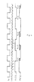
- the fractional frequencies that is the interpolated frequencies. They are established. They are produced by delaying whole pulses by means of partial fractions k1 and k2.
- the coefficient k1 and k2 must be updated cyclically for each pulse.
- the topmost pulse sequence illustrates the reference frequency pulse sequence.
- the pulse sequence second from the top represents the frequency 4 ⁇ f o produced in the delay register in block 9.
- integer divisor frequencies are produced in the synthesizer.
- the first pulse is lengthened as shown in the figure, by a time which corresponding to k1 pulses produced in block 9.
- the coefficients are a cyclical series 0, 1, 2, 3, 0, 1, 2,...
- the cyclic updated coefficients are 7, 14, 21, 28, 35, 42, 49, 56, 63, 6, 13, 20...
- Fig. 5 presents schematically the production of delays smaller than the single delay in the delay chain of Fig. 3, that is, of fractions of the single delay from the single delays of two delay chains having different frequencies.
- the stepped delay curves 51 and 52 represent the frequencies multiplied by coefficients L and L+ ⁇ L
- the time difference of the delay curves in the x axis direction represents the difference of the starting times.
- the desired delay difference containing also fractions of the single delays is obtained, for instance in the present case, as the difference of the delays corresponding to point P1 on curve 51 and P2 on curve 52.
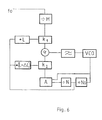
- Figure 6 is an embodiment alternative to that of Fig. 2. From the equilibrium equation of its phase detector the frequency f x is derived: The smallest frequency change is that is, the frequency raster becomes divided into fractions similar to those in the form of Fig. 2, and in practice, even of the same size. However, the embodiment of Fig. 6 is inferior to the embodiment in the respect of Fig. 2 that in it the variable frequency f x is multiplied, for which reason it is less stable.
- the blocks 8 and 9 have applied to them the reference signal f o but it will be appreciated by a person skilled in the art that instead, the output of the VCO 5, either directly or via the divider 6, or the output of the divider 1 may be applied. As regards the embodiment of Fig. 6, the blocks 8 and 9 may have applied to them the output of the VCO direct or via the off-set counter A, or the output of the M divider instead of the VCO output signal via the divider N o .
- the present invention enables the drift of the reference frequency to be compensated and/or small frequency steps to be established utilizing the internal logic of the synthesizer. By the aid of multiplications and divisions, frequencies lying between integer frequencies can be generated.
- the invention can be applied in all instances in which new reference frequencies are produced from a reference frequency with a synthesizer. An application of this kind is for instance the transmitter/receiver component of a radio telephone.
Landscapes
- Stabilization Of Oscillater, Synchronisation, Frequency Synthesizers (AREA)
- Superheterodyne Receivers (AREA)
- Channel Selection Circuits, Automatic Tuning Circuits (AREA)
- Organic Low-Molecular-Weight Compounds And Preparation Thereof (AREA)
Applications Claiming Priority (2)
| Application Number | Priority Date | Filing Date | Title |
|---|---|---|---|
| FI900303A FI87032C (fi) | 1990-01-18 | 1990-01-18 | Interpolerande pll-frekvenssyntetiserare |
| FI900303 | 1990-01-18 |
Publications (3)
| Publication Number | Publication Date |
|---|---|
| EP0438309A2 true EP0438309A2 (de) | 1991-07-24 |
| EP0438309A3 EP0438309A3 (en) | 1991-12-04 |
| EP0438309B1 EP0438309B1 (de) | 1995-09-20 |
Family
ID=8529739
Family Applications (1)
| Application Number | Title | Priority Date | Filing Date |
|---|---|---|---|
| EP91300361A Expired - Lifetime EP0438309B1 (de) | 1990-01-18 | 1991-01-17 | Interpolierender Frequenzsynthetisierer mit Phasenregelkeis |
Country Status (6)
| Country | Link |
|---|---|
| US (1) | US5079520A (de) |
| EP (1) | EP0438309B1 (de) |
| JP (1) | JP3075418B2 (de) |
| AT (1) | ATE128293T1 (de) |
| DE (1) | DE69113070T2 (de) |
| FI (1) | FI87032C (de) |
Cited By (4)
| Publication number | Priority date | Publication date | Assignee | Title |
|---|---|---|---|---|
| EP0560475A1 (de) * | 1992-03-09 | 1993-09-15 | Nokia Mobile Phones Ltd. | Verfahren und Vorrichtung zum Auswählen der optimalen Empfangsfrequenz in einem Vielkanalempfänger |
| EP0550249A3 (en) * | 1991-12-31 | 1993-11-10 | Nokia Mobile Phones Ltd | Modulation method and circuit arrangement |
| EP1274181A1 (de) * | 2001-07-05 | 2003-01-08 | Alps Electric Co., Ltd. | Empfänger mit mehreren Antennen zur Verbesserung des Signal/Störverhältnis durch Einstellung der Phasen der Antennensignale |
| CN103957007A (zh) * | 2014-05-09 | 2014-07-30 | 武汉工程大学 | 低信噪比下任意波形的微弱信号检测方法及系统 |
Families Citing this family (14)
| Publication number | Priority date | Publication date | Assignee | Title |
|---|---|---|---|---|
| US5281863A (en) * | 1992-03-26 | 1994-01-25 | Intel Corporation | Phase-locked loop frequency-multiplying phase-matching circuit with a square-wave output |
| US5699387A (en) * | 1993-06-23 | 1997-12-16 | Ati Technologies Inc. | Phase offset cancellation technique for reducing low frequency jitters |
| FI98420C (fi) * | 1995-01-24 | 1997-06-10 | Nokia Mobile Phones Ltd | Menetelmä ja kytkentä moduloidun signaalin muodostamiseksi lähetin/vastaanottimessa |
| FI951918A7 (fi) * | 1995-04-21 | 1996-10-22 | Nokia Mobile Phones Ltd | Lähetin-vastaanotinlaite ja menetelmä kompleksien I/Q-signaalin synnyttämiseksi ja käsittelemiseksi |
| US5787362A (en) * | 1996-07-08 | 1998-07-28 | Nokia Mobile Phones Limited | AM removal from FM signal generated by IQ modulator |
| US5768691A (en) * | 1996-08-07 | 1998-06-16 | Nokia Mobile Phones Limited | Antenna switching circuits for radio telephones |
| GB2317512B (en) * | 1996-09-12 | 2001-01-24 | Nokia Mobile Phones Ltd | Frequency modulation using a phase-locked loop |
| US6373912B1 (en) * | 1997-06-16 | 2002-04-16 | Legerity, Inc. | Phase-locked loop arrangement with fast lock mode |
| US6160456A (en) * | 1999-06-14 | 2000-12-12 | Realtek Semiconductor Corp. | Phase-locked loop having adjustable delay elements |
| US6356132B1 (en) | 2000-01-31 | 2002-03-12 | Agere Systems Guardian Corp. | Programmable delay cell |
| US6806750B1 (en) * | 2002-04-23 | 2004-10-19 | National Semiconductor Corporation | Method and system for clock deskewing using a continuously calibrated delay element in a phase-locked loop |
| US7002417B2 (en) * | 2003-03-21 | 2006-02-21 | Nokia Corporation | RC and SC filter compensation in a radio transceiver |
| US20040227578A1 (en) * | 2003-05-14 | 2004-11-18 | Miikka Hamalainen | Acoustic resonance-based frequency synthesizer using at least one bulk acoustic wave (BAW) or thin film bulk acoustic wave (FBAR) device |
| US7196564B2 (en) * | 2005-07-22 | 2007-03-27 | Texas Instruments Incorporated | High frequency balanced phase interpolator |
Family Cites Families (5)
| Publication number | Priority date | Publication date | Assignee | Title |
|---|---|---|---|---|
| DE3165323D1 (en) * | 1981-03-06 | 1984-09-13 | Itt Ind Gmbh Deutsche | Delay circuit with integrated insulated-layer field-effect transistor for digital signals, and application of the same to colour television receivers |
| US4611230A (en) * | 1984-12-18 | 1986-09-09 | Zenith Electronics Corporation | Vertical video centering control system |
| SE447618B (sv) * | 1985-04-12 | 1986-11-24 | Ericsson Telefon Ab L M | Sett och anordning for att faslasa en styrd oscillators signal till en referensoscillators signal |
| US4802009A (en) * | 1987-07-13 | 1989-01-31 | Rca Licensing Corporation | Digitally controlled phase locked loop system |
| US4868524A (en) * | 1988-10-20 | 1989-09-19 | The Johns Hopkins University | RF circuit utilizing a voltage controlled saw oscillator |
-
1990
- 1990-01-18 FI FI900303A patent/FI87032C/fi not_active IP Right Cessation
-
1991
- 1991-01-07 US US07/638,130 patent/US5079520A/en not_active Expired - Lifetime
- 1991-01-17 EP EP91300361A patent/EP0438309B1/de not_active Expired - Lifetime
- 1991-01-17 AT AT91300361T patent/ATE128293T1/de active
- 1991-01-17 DE DE69113070T patent/DE69113070T2/de not_active Expired - Fee Related
- 1991-01-18 JP JP03004372A patent/JP3075418B2/ja not_active Expired - Fee Related
Cited By (7)
| Publication number | Priority date | Publication date | Assignee | Title |
|---|---|---|---|---|
| EP0550249A3 (en) * | 1991-12-31 | 1993-11-10 | Nokia Mobile Phones Ltd | Modulation method and circuit arrangement |
| US5325075A (en) * | 1991-12-31 | 1994-06-28 | Nokia Mobile Phones Ltd. | Method and circuit arrangement to generate a phase modulated or frequency modulated signal |
| EP0560475A1 (de) * | 1992-03-09 | 1993-09-15 | Nokia Mobile Phones Ltd. | Verfahren und Vorrichtung zum Auswählen der optimalen Empfangsfrequenz in einem Vielkanalempfänger |
| US5649320A (en) * | 1992-03-09 | 1997-07-15 | Nokia Mobile Phones Ltd. | Automatic frequency control loop and temperature compensation for a receiver |
| EP1274181A1 (de) * | 2001-07-05 | 2003-01-08 | Alps Electric Co., Ltd. | Empfänger mit mehreren Antennen zur Verbesserung des Signal/Störverhältnis durch Einstellung der Phasen der Antennensignale |
| US6925294B2 (en) | 2001-07-05 | 2005-08-02 | Alps Electric Co., Ltd. | Antenna receiver in which carrier-to-noise ratio of demodulation signal is improved |
| CN103957007A (zh) * | 2014-05-09 | 2014-07-30 | 武汉工程大学 | 低信噪比下任意波形的微弱信号检测方法及系统 |
Also Published As
| Publication number | Publication date |
|---|---|
| FI87032B (fi) | 1992-07-31 |
| JPH0799447A (ja) | 1995-04-11 |
| FI900303A0 (fi) | 1990-01-18 |
| ATE128293T1 (de) | 1995-10-15 |
| JP3075418B2 (ja) | 2000-08-14 |
| EP0438309A3 (en) | 1991-12-04 |
| DE69113070D1 (de) | 1995-10-26 |
| EP0438309B1 (de) | 1995-09-20 |
| DE69113070T2 (de) | 1996-05-02 |
| US5079520A (en) | 1992-01-07 |
| FI87032C (fi) | 1992-11-10 |
| FI900303L (fi) | 1991-07-19 |
Similar Documents
| Publication | Publication Date | Title |
|---|---|---|
| EP0438309B1 (de) | Interpolierender Frequenzsynthetisierer mit Phasenregelkeis | |
| US6281759B1 (en) | Digital frequency generation method and apparatus | |
| US5781054A (en) | Digital phase correcting apparatus | |
| EP0479969B1 (de) | Synthesizer mit gebrochenem teilverhältnis für ein sprach-/daten-kommunikationssystem | |
| CA2284842A1 (en) | Frequency synthesis circuit tuned by digital words | |
| EP0800276A1 (de) | Frequenzvervielfacher, bei dem das Multiplikationsverhältnis in der ersten Stufe grösser ist als in den nachfolgenden Stufen | |
| JPH11234122A (ja) | ディジタルpll回路とクロックの生成方法 | |
| US4603304A (en) | Reference frequency generation for split-comb frequency synthesizer | |
| JPS6256689B2 (de) | ||
| US3546617A (en) | Digital frequency synthesizer | |
| CN101371439A (zh) | 相位比较电路及使用该相位比较电路的pll频率合成器 | |
| EP0565362B1 (de) | Frequenzabstimmung mit Frequenzsynthesierer | |
| US4008443A (en) | Quaternary frequency synthesizer | |
| EP0563400A1 (de) | Frequenzkonverter, mehrstufiger frequenzkonverter und frequenzsynthetisierer mit solchen konvertern | |
| JPS62210731A (ja) | 周波数シンセサイザ | |
| EP0454955B1 (de) | Schaltung zur Erzeugung eines Abtasttaktes | |
| CA1260563A (en) | Frequency synthesizer of a phase-locked type with a sampling circuit | |
| US4871981A (en) | Fast hopping microwave frequency synthesizer | |
| JPS5881337A (ja) | 周波数シンセサイザ | |
| EP0223812A1 (de) | Phasenmodulatoren | |
| AU642027B2 (en) | Multiloop microwave frequency synthesizer with low phase noise | |
| SU1169184A1 (ru) | Устройство синхронизаций | |
| SU1042188A1 (ru) | Цифровой синтезатор частот | |
| JPS6333739B2 (de) | ||
| JPS573438A (en) | Synthesizer type channel selector |
Legal Events
| Date | Code | Title | Description |
|---|---|---|---|
| PUAI | Public reference made under article 153(3) epc to a published international application that has entered the european phase |
Free format text: ORIGINAL CODE: 0009012 |
|
| AK | Designated contracting states |
Kind code of ref document: A2 Designated state(s): AT BE CH DE DK ES FR GB GR IT LI LU NL SE |
|
| PUAL | Search report despatched |
Free format text: ORIGINAL CODE: 0009013 |
|
| AK | Designated contracting states |
Kind code of ref document: A3 Designated state(s): AT BE CH DE DK ES FR GB GR IT LI LU NL SE |
|
| 17P | Request for examination filed |
Effective date: 19920528 |
|
| 17Q | First examination report despatched |
Effective date: 19940502 |
|
| GRAA | (expected) grant |
Free format text: ORIGINAL CODE: 0009210 |
|
| AK | Designated contracting states |
Kind code of ref document: B1 Designated state(s): AT BE CH DE DK ES FR GB GR IT LI LU NL SE |
|
| PG25 | Lapsed in a contracting state [announced via postgrant information from national office to epo] |
Ref country code: LI Effective date: 19950920 Ref country code: GR Free format text: LAPSE BECAUSE OF FAILURE TO SUBMIT A TRANSLATION OF THE DESCRIPTION OR TO PAY THE FEE WITHIN THE PRESCRIBED TIME-LIMIT Effective date: 19950920 Ref country code: ES Free format text: THE PATENT HAS BEEN ANNULLED BY A DECISION OF A NATIONAL AUTHORITY Effective date: 19950920 Ref country code: DK Effective date: 19950920 Ref country code: CH Effective date: 19950920 Ref country code: BE Effective date: 19950920 Ref country code: AT Effective date: 19950920 |
|
| REF | Corresponds to: |
Ref document number: 128293 Country of ref document: AT Date of ref document: 19951015 Kind code of ref document: T |
|
| REF | Corresponds to: |
Ref document number: 69113070 Country of ref document: DE Date of ref document: 19951026 |
|
| ET | Fr: translation filed | ||
| ITF | It: translation for a ep patent filed | ||
| PG25 | Lapsed in a contracting state [announced via postgrant information from national office to epo] |
Ref country code: LU Free format text: LAPSE BECAUSE OF NON-PAYMENT OF DUE FEES Effective date: 19960131 |
|
| REG | Reference to a national code |
Ref country code: CH Ref legal event code: PL |
|
| PLBE | No opposition filed within time limit |
Free format text: ORIGINAL CODE: 0009261 |
|
| STAA | Information on the status of an ep patent application or granted ep patent |
Free format text: STATUS: NO OPPOSITION FILED WITHIN TIME LIMIT |
|
| 26N | No opposition filed | ||
| REG | Reference to a national code |
Ref country code: GB Ref legal event code: IF02 |
|
| REG | Reference to a national code |
Ref country code: GB Ref legal event code: 732E |
|
| PGFP | Annual fee paid to national office [announced via postgrant information from national office to epo] |
Ref country code: SE Payment date: 20040107 Year of fee payment: 14 |
|
| PGFP | Annual fee paid to national office [announced via postgrant information from national office to epo] |
Ref country code: FR Payment date: 20040108 Year of fee payment: 14 |
|
| PGFP | Annual fee paid to national office [announced via postgrant information from national office to epo] |
Ref country code: GB Payment date: 20040114 Year of fee payment: 14 |
|
| PGFP | Annual fee paid to national office [announced via postgrant information from national office to epo] |
Ref country code: NL Payment date: 20040121 Year of fee payment: 14 |
|
| PGFP | Annual fee paid to national office [announced via postgrant information from national office to epo] |
Ref country code: DE Payment date: 20040129 Year of fee payment: 14 |
|
| PG25 | Lapsed in a contracting state [announced via postgrant information from national office to epo] |
Ref country code: IT Free format text: LAPSE BECAUSE OF NON-PAYMENT OF DUE FEES;WARNING: LAPSES OF ITALIAN PATENTS WITH EFFECTIVE DATE BEFORE 2007 MAY HAVE OCCURRED AT ANY TIME BEFORE 2007. THE CORRECT EFFECTIVE DATE MAY BE DIFFERENT FROM THE ONE RECORDED. Effective date: 20050117 Ref country code: GB Free format text: LAPSE BECAUSE OF NON-PAYMENT OF DUE FEES Effective date: 20050117 |
|
| PG25 | Lapsed in a contracting state [announced via postgrant information from national office to epo] |
Ref country code: SE Free format text: LAPSE BECAUSE OF NON-PAYMENT OF DUE FEES Effective date: 20050118 |
|
| PG25 | Lapsed in a contracting state [announced via postgrant information from national office to epo] |
Ref country code: NL Free format text: LAPSE BECAUSE OF NON-PAYMENT OF DUE FEES Effective date: 20050801 |
|
| PG25 | Lapsed in a contracting state [announced via postgrant information from national office to epo] |
Ref country code: DE Free format text: LAPSE BECAUSE OF NON-PAYMENT OF DUE FEES Effective date: 20050802 |
|
| EUG | Se: european patent has lapsed | ||
| GBPC | Gb: european patent ceased through non-payment of renewal fee |
Effective date: 20050117 |
|
| PG25 | Lapsed in a contracting state [announced via postgrant information from national office to epo] |
Ref country code: FR Free format text: LAPSE BECAUSE OF NON-PAYMENT OF DUE FEES Effective date: 20050930 |
|
| NLV4 | Nl: lapsed or anulled due to non-payment of the annual fee |
Effective date: 20050801 |
|
| REG | Reference to a national code |
Ref country code: FR Ref legal event code: ST |