EP0439227B1 - Halbleiteranordnung mit einem Träger, Verfahren zu seiner Herstellung, und Verfahren zum Herstellen des Trägers - Google Patents
Halbleiteranordnung mit einem Träger, Verfahren zu seiner Herstellung, und Verfahren zum Herstellen des Trägers Download PDFInfo
- Publication number
- EP0439227B1 EP0439227B1 EP91200094A EP91200094A EP0439227B1 EP 0439227 B1 EP0439227 B1 EP 0439227B1 EP 91200094 A EP91200094 A EP 91200094A EP 91200094 A EP91200094 A EP 91200094A EP 0439227 B1 EP0439227 B1 EP 0439227B1
- Authority
- EP
- European Patent Office
- Prior art keywords
- groove
- conductors
- semiconductor
- semiconductor elements
- support rod
- Prior art date
- Legal status (The legal status is an assumption and is not a legal conclusion. Google has not performed a legal analysis and makes no representation as to the accuracy of the status listed.)
- Expired - Lifetime
Links
Images

Classifications
-
- H—ELECTRICITY
- H10—SEMICONDUCTOR DEVICES; ELECTRIC SOLID-STATE DEVICES NOT OTHERWISE PROVIDED FOR
- H10W—GENERIC PACKAGES, INTERCONNECTIONS, CONNECTORS OR OTHER CONSTRUCTIONAL DETAILS OF DEVICES COVERED BY CLASS H10
- H10W72/00—Interconnections or connectors in packages
-
- H—ELECTRICITY
- H10—SEMICONDUCTOR DEVICES; ELECTRIC SOLID-STATE DEVICES NOT OTHERWISE PROVIDED FOR
- H10W—GENERIC PACKAGES, INTERCONNECTIONS, CONNECTORS OR OTHER CONSTRUCTIONAL DETAILS OF DEVICES COVERED BY CLASS H10
- H10W70/00—Package substrates; Interposers; Redistribution layers [RDL]
- H10W70/60—Insulating or insulated package substrates; Interposers; Redistribution layers
- H10W70/62—Insulating or insulated package substrates; Interposers; Redistribution layers characterised by their interconnections
- H10W70/65—Shapes or dispositions of interconnections
- H10W70/658—Shapes or dispositions of interconnections for devices provided for in groups H10D8/00 - H10D48/00
-
- H—ELECTRICITY
- H10—SEMICONDUCTOR DEVICES; ELECTRIC SOLID-STATE DEVICES NOT OTHERWISE PROVIDED FOR
- H10W—GENERIC PACKAGES, INTERCONNECTIONS, CONNECTORS OR OTHER CONSTRUCTIONAL DETAILS OF DEVICES COVERED BY CLASS H10
- H10W70/00—Package substrates; Interposers; Redistribution layers [RDL]
- H10W70/60—Insulating or insulated package substrates; Interposers; Redistribution layers
- H10W70/62—Insulating or insulated package substrates; Interposers; Redistribution layers characterised by their interconnections
- H10W70/65—Shapes or dispositions of interconnections
- H10W70/657—Shapes or dispositions of interconnections on sidewalls or bottom surfaces of the package substrates, interposers or redistribution layers
-
- H—ELECTRICITY
- H10—SEMICONDUCTOR DEVICES; ELECTRIC SOLID-STATE DEVICES NOT OTHERWISE PROVIDED FOR
- H10W—GENERIC PACKAGES, INTERCONNECTIONS, CONNECTORS OR OTHER CONSTRUCTIONAL DETAILS OF DEVICES COVERED BY CLASS H10
- H10W70/00—Package substrates; Interposers; Redistribution layers [RDL]
- H10W70/60—Insulating or insulated package substrates; Interposers; Redistribution layers
- H10W70/67—Insulating or insulated package substrates; Interposers; Redistribution layers characterised by their insulating layers or insulating parts
- H10W70/68—Shapes or dispositions thereof
-
- H—ELECTRICITY
- H10—SEMICONDUCTOR DEVICES; ELECTRIC SOLID-STATE DEVICES NOT OTHERWISE PROVIDED FOR
- H10W—GENERIC PACKAGES, INTERCONNECTIONS, CONNECTORS OR OTHER CONSTRUCTIONAL DETAILS OF DEVICES COVERED BY CLASS H10
- H10W72/00—Interconnections or connectors in packages
- H10W72/01—Manufacture or treatment
- H10W72/0198—Manufacture or treatment batch processes
Definitions
- the invention relates to a semiconductor device comprising a support with a surface provided with a groove having sidewalls on which conductors are present, which conductors extend onto the surface of the support, and with a semiconductor element which is present in the groove and makes electrical contact with the conductors on the sidewalls.
- the invention further relates to a method of manufacturing such a device and to a method of manufacturing a support rod which can be used for the manufacture of the semiconductor device.
- Such a device can be used as a "surface mounting device”.
- the support can be fastened on a PC-board, the conductors present on the support then making electrical contact with conductors on the PC-board.
- British Patent no. 1597707 discloses a device of the kind mentioned in the opening paragraph in which a semiconductor element is mounted in a V-shaped groove.
- the semiconductor element is fastened to a conductor on one of the walls and connected to the conductor on the other wall by means of a connection wire.
- the known device described has the disadvantage that separate process steps are required for fastening the semiconductor element on the support and for providing the connection wire. Since the walls of the groove are oblique and since the semiconductor element in practice has very small dimensions, these process steps are in addition difficult to carry out.
- the invention has for its object inter alia to counteract the disadvantages described.
- the device is characterized in that the semiconductor element is clamped and located entirely within in the groove with one of its main surfaces parallel to a sidewall of the groove, thus making electrical contact with the conductors on the sidewalls, and the groove is filled with a protective material, so that the semiconductor device constitutes a surface mounting device with the conductors extending from the groove as connection means for surface mounting. Since the semiconductor element is clamped between the conductors on the walls, it is achieved that both a mechanical and an electrical connection is effected between the semiconductor element and the support in a single process step and in a simple manner. Thanks to this simple manner of effecting a connection between the support and the semiconductor element, it is also possible to use very small semiconductor elements in such a semiconductor device.
- US 4,670,770 describes a multi-chip-module (MCM) which meets the features given in the preamble of Claim 1 and has a semiconductor element with beveled edges provided in a matching groove in a semiconductor substrate.
- MCM multi-chip-module
- US 4,922,378 discloses a semiconductor device comprising a support provided with a groove and with a semiconductor element which is placed with a small edge portion in the groove. There are, however, no conductors present on the walls of the groove, nor is the semiconductor element clamped in the groove. Moreover, the device is not usable as a surface mounting device.
- the semiconductor elements may be clamped in the groove in that the support is so deformed that the groove is bent open, the semiconductor elements are inserted into the groove, and the support is allowed to spring back. It is also possible to heat the support, the groove becoming larger through expansion, upon which the semiconductor elements can be inserted, after which the semiconductor elements are clamped in through contraction of the groove during cooling-down, and an electrical connection is created.
- the device according to the invention is characterized in that the groove has a tapering shape with a cross-section which becomes smaller in downward direction, in which groove the semiconductor element is automatically held with clamping fit. It is achieved in this way that the semiconductor device can be manufactured by simply pushing the semiconductor element into the groove.
- the semiconductor device is characterized in that the walls of the groove enclose an angle of 5 to 15°. If the walls of the groove enclose an angle smaller than approximately 5°, it appears in practice during the manufacture of the support that the groove occasionally fails to exhibit a tapering shape owing to tolerances on the groove dimensions. The semiconductor element is not satisfactorily clamped in the groove in the case of an angle greater than approximately 15°.
- a more secure connection between semiconductor element and support may be obtained in that one of the conductors or the semiconductor element is provided with a solder layer before the semiconductor element is inserted, in that then the semiconductor element is inserted, upon which the semiconductor device thus created is heated.
- a soldered connection is provided between the semiconductor element and the conductor in this way.
- a deformable contact body is provided between the semiconductor element and one of the conductors in the groove. High mechanical stresses which may occur between the support and the semiconductor element during insertion and during operation of the semiconductor element can be absorbed by this contact body.
- a metal layer provided by electrodeposition or a drop of conducting glue may be used as the deformable contact body.
- the deformable contact body is a bump contact provided on the semiconductor element.
- Such a bump contact is provided through wire bonding. This means that a wire is bonded to a connection surface of the semiconductor element and then broken off close to the connection surface.
- Such a bump contact preferably made of gold or silver, can be manufactured in known manner on existing machines and is capable of satisfactorily absorbing the said stresses, as has been demonstrated in practice.
- the invention further r lates to a method of manufacturing a device as mentioned in the opening paragraph.
- a method is also known from US-A-4,670,770.
- this method is characterized in that it starts with a support rod with a surface provided with a continuous groove extending along the rod and having sidewalls on which electrical conductors are present, which conductors extend onto the surface of the support rod so as to constitute connection means for surface mounting, that thereafter semiconductor elements are inserted entirely into the groove with a clamping fit, whereby one of the main surfaces of the semiconductor elements is parallel to a sidewall of the groove, and that the groove is filled with a protective material, upon which the support rod is subdivided in a number of semiconductor devices.
- the support rod may be manufactured in a simple manner from a ceramic material by, for example, a sintering process, from a synthetic material by, for example, an injection-moulding process, from a metal covered with an insulating material, such as anodized aluminium, by, for example, an extrusion process, or from a glass by, for example, drawing of a rod.
- a semiconductor element can be fixed and contacted on a support which is suitable for SMD mounting in a simple and inexpensive manner by means of the method.
- the groove is filled with a protective lacquer to protect the semiconductor element from atmospheric influences.
- the semiconductor elements are mounted before the support rod is subdivided.
- the groove is formed to have a tapering shape with a cross-section which becomes smaller in downward direction, where the semiconductor elements are provided in the groove with clamping fit by being pushed into the groove.
- the dimensions of the groove are such during this that a semiconductor element achieves a pressure contact in the tapering portion of the groove and thus makes an electrical connection. In this way the semiconductor elements can be fastened and contacted in the groove simply by being pushed into this groove.
- a solder layer is provided on the conductors or on the semiconductor elements before the semiconductor elements are inserted into the groove, while the support rod with semiconductor elements is heated after the semiconductor elements have been inserted. If a temperature above the melting point of the solder layer is achieved during this, the solder layer will flow and a soldered joint will be made. If the temperature remains below the melting point of the solder layer, a thermocompression connection will be made. Such a more secure connection is thus realised in a very simple manner.
- deformable contact bodies are provided on the semiconductor elements before the semiconductor elements are inserted into the groove.
- the contact body can then be provided in a simple manner because the surface of the semiconductor element is readily accessible.
- the contact bodies are provided on the semiconductor elements while the latter are still on a semiconductor slice, after which the slice is divided into individual semiconductor elements which are inserted into the groove.
- a contact body can be provided on each semiconductor element in a simple manner by means of usual machines, since the semiconductor elements assume fixed, well-defined positions on the slice.
- the invention relates also to a method of manufacturing a support rod as defined in Claim 13.
- the sidewalls of the groove of the support rod can be provided with conductors in a certain pattern, so that also semiconductor elements having more than two contacts, such as, for example, transistors and ICs, can be connected through the provision of several conductors on one wall.
- the conductors may be provided onto the main surface of the support rod in a simple manner in the following sequence:
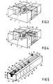
- Fig. 1 shows a first embodiment of a semiconductor device according to the invention.
- This device as well as the devices yet to be described below are typically suitable for surface mounting; they are often designated “surface mounting device” or SMD.
- Fig. 1 shows a semiconductor device comprising a support 1 provided with a continuous groove 2 having walls 3 and 4, on which walls metal conductors 6 and 7 are present, which conductors extend to on the support, and comprising a semiconductor element which is inside the groove and makes electrical contact with the conductors on the walls.
- the walls 3 and 4 of the groove enclose an angle of approximately 10°.
- the conductors 6 and 7 run from the groove 2 over an upper surface 5 to a side surface 8 of the support, and possibly further to a lower surface 10.
- the conductors 6 and 7 can make electrical contact with conductors on a PC-board.
- a semiconductor element 11 is provided in the groove 2, in the embodiment shown a semiconductor diode. The semiconductor element is clamped in the groove 2, thereby making electrical contact with conductors 6 and 7 on the walls 3 and 4. A mechanical as well as an electrical contact has thus been effected. It is not necessary, accordingly, to include separate process steps for making mechanical and electrical contact in a production process for the device according to the invention.
- the groove 2 is filled with a protective lacquer 13, for example an epoxy resin applied in the liquid state, after the semiconductor element 11 has been inserted. It is also possible to provide a glass over the semiconductor element as an alternative to the protective lacquer.
- the support 1 is formed from a ceramic material, a synthetic material, a metal covered with an insulating material, or a glass.
- the semiconductor element 11 can be automatically provided with clamping fit in that the element is pushed into the groove 2.
- the groove 2 has a tapering shape with a cross-section which becomes smaller in downward direction, so that the semiconductor element can be automatically provided and inserted with clamping fit.
- Fig. 2 shows a cross-section of the support 1.
- the walls 3 and 4 of the groove 2 preferably enclose an angle 15 of 5 to 15°. If the angle 15 is smaller than approximately 5°, it is found in practice during manufacture of the support that the groove ocasionally fails to have a tapering shape owing to tolerances on the groove dimensions. In the case of an angle greater than approximately 15°, the semiconductor element cannot be securely clamped in the groove.
- FIG. 1 shows an embodiment in which walls 3 and 4 enclose an angle of approximately 10°, while both walls enclose an angle of approximately 95° with the upper surface 5.
- Fig. 3 shows an alternative embodiment in which wall 3 is substantially perpendicular to the upper surface and wall 4 encloses an angle of approximately 100° with the upper surface 5.
- a more secure connection between semiconductor element 11 and support 1 may be obtained in that the conductors 6 and 7 and the semiconductor element 11 are provided with solder layers 66, 77 and 116, respectively, (see Fig. 2) of, for example, a usual lead-tin alloy before the semiconductor element 11 is inserted, in that then the semiconductor element is inserted, and the semiconductor device thus created is heated.
- a soldered connection is provided between the semiconductor element and the conductor in this way. It should be noted that the solder layer is indeed drawn on the conductors 6 and 7 and on the semiconductor element 11, but that a more secure connection is also obtained already if this solder layer should be present on only one of the conductors or on the semiconductor element only.
- a deformable contact body 12 is used between the semiconductor element and one of the conductors in the groove in order to prevent high mechanical stresses occurring during positioning of the semiconductor element and during operation.
- a contact body is a bump contact provided on the semiconductor element through wire bonding, i.e. a wire is bonded to a connection surface of the semiconductor element and subsequently broken off close to the connection surface.
- Such a bump contact preferably made of gold or silver, may be manufactured in known manner on existing machines and is capable of absorbing the said stresses satisfactorily, as has been shown in practice.
- the semiconductor device may be connected to a PC-board with its lower side 10 as well as with its upper side 5.
- the groove is provided in a continuous recess 14 in the support (see Figs. 1 and 2).
- Such a recess may be used to hold a drop of glue (not drawn).
- the semiconductor device may then be fixed to a PC-board with its upper side 5 by means of this drop of glue before the semiconductor device is fixed by soldering.
- the recess 14 ensures that the upper surface 5 of the semiconductor device merges well with a surface of the PC-board in spite of the drop of glue, so that a proper soldered joint between conductors present on the upper surface 5 and the side surfaces 8 of the semiconductor device and on the PC-board can be made.
- Fig. 1 shows a semiconductor device comprising a diode.
- the support may also be used, for example, for a transistor or IC, as shown in Fig. 4.
- the contact at a rear side of the semiconductor element may then be the collector contact which is in connection with conductor 6.
- two bump contacts 112 and 212 made of gold may then be present, being the base contact and the emitter contact, which will be in connection with two mutually separated conductors 17 and 27.
- the dimensions of the semiconductor devices manufactured by means of the invention can be very small; for example, the dimensions of the supports for diodes and transistors are 2 mm x 1,25 mm x 1,2 mm (known as 0805 in SMD technology) or 1,5 mm x 0,75 mm x 0,8 mm (known as 0603).
- Fig. 5 shows a step in the production process.
- the process starts with a support rod 51 provided with a continuous groove 52 having walls 53 and 54 on which electrical conductors 56 and 57 are present, which conductors extend onto the surface of the support rod 51.
- the support rod is provided with a continuous recess 64.
- the support rod may be made of a ceramic material, such as, for example, silicon carbide, silicon nitride, or aluminium oxide.
- Such a support rod is manufactured, for example, in a sintering process.
- a support rod made of a thermoplastic synthetic material is obtained in known manner, for example, through injection moulding or extrusion.
- the support rod 51 is constructed as a regular body, the continuous groove 2 and the continuous recess 64 run in the extrusion direction. Synthetic materials suitable for this are, for example, polyether-sulfon (PES) or polyetherimide (PEI). The so-called liquid crystal polymers are also suitable.
- the support rod may also consist of a glass. Such a support rod may be obtained, for example, by drawing or by other methods known in glass technology.
- a number of semiconductor elements 11 can be provided in the groove 52. These semiconductor elements are inserted next to one another in the groove with clamping fit.
- the elements 11 thereby come into pressure contact with the conductors 56 and 57 on the walls 53 and 54 of the support rod 51.
- the semiconductor elements are covered with a protective lacquer 63, drawn in part in Fig. 5, after which the support rod 51 is subdivided into several semiconductor devices along the broken lines 65 by, for example, sawing or breaking. It is possible thereby to make semiconductor devices consisting of a support provided with one semiconductor element, but also semiconductor devices consisting of a support provided with several semiconductor elements. In the latter semiconductor devices, the conductors 56 and 57 are usually subdivided into several conductor tracks which connect the individual semiconductor elements.
- the semiconductor elements may be provided in various ways.
- the semiconductor element will be included under tension in the groove and an electrical connection will be formed in that the support rod 51 is so deformed that the groove 52 is bent slightly open, upon which the semiconductor elements 11 are inserted and the support body is allowed to spring back.
- the support rod is provided with a tapering groove whose cross-section decreases in downward direction and in which the semiconductor elements can be automatically provided with clamping fit (see Figs. 2 and 5).
- a solder layer of a usual lead-tin alloy is provided on the conductors 56, 57 and on the semiconductor elements 11 before the semiconductor elements are inserted in the groove, which solder layer is not drawn in Fig. 5 for reasons of clarity (these solder layers are identical to the solder layers 66, 67 and 116 indicated in Fig. 2).
- the support rod comprising semiconductor elements is heated. If a temperature above the melting point of the solder layer is reached during this, the solder layer will flow and a soldered joint will be made. If the temperature remains below the melting point of the solder layer, a thermocompression connection will be made. A more secure connection as described is thus realised in a very simple manner.
- a deformable contact body 12 is provided on the semiconductor element 11 before the semiconductor elements are provided in the groove 2.
- the deformable contact body is capable of absorbing the high stresses which occur during insertion of the semiconductor element and during operation of the semiconductor device.
- the contact bodies 12 are preferably provided on the semiconductor elements 11 while these semiconductor elements are still on a semiconductor slice. This can be done, for example, by electrochemically providing a metal layer, thickening the latter and etching it into a pattern, or by providing a drop of conducting glue.
- a bump contact is provided through wire bonding with a conventional wire bonding machine, a small wire being bonded to a connection surface of the semiconductor elements, which wire is subsequently broken off close to the connection surface.
- the semiconductor slice is then subdivided into separate semiconductor elements 11, each provided with a bump contact 12, by means of conventional techniques such as, for example, sawing.
- the invention also relates to a method of manufacturing a support rod 51 which is suitable for accommodating semiconductor elements 11 and which is provided with a continuous groove 52 having walls 53 and 54 on which conductors 56 and 57 are present, which conductors extend to on the support rod 51.
- the conductors according to the invention are provided on the support rod in the following sequence:
Landscapes
- Wire Bonding (AREA)
- Die Bonding (AREA)
- Structures Or Materials For Encapsulating Or Coating Semiconductor Devices Or Solid State Devices (AREA)
Claims (14)
- Halbleiteranordnung mit einem Träger, welcher mit einer Oberfläche versehen ist, die eine Vertiefung mit Seitenwänden aufweist, auf welchen Leiter angeordnet sind, welche sich auf der Oberfläche des Trägers erstrecken, sowie mit einem Halbleiterelement, welches in der Vertiefung vorgesehen ist und einen elektrischen Kontakt mit den Leitern auf den Seitenwänden herstellt, dadurch gekennzeichnet, daß das Halbleiterelement mit einer seiner Hauptoberflächen parallel zu einer Seitenwand der Vertiefung gänzlich in der Vertiefung festgeklemmt und angeordnet ist, wodurch ein elektrischer Kontakt mit den Leitern auf den Seitenwänden hergestellt wird, und die Vertiefung mit einem Schutzmaterial gefüllt wird, so daß die Halbleiteranordnung ein für Oberflächenmontage ausgelegtes Bauelement darstellt, wobei sich die Leiter von der Vertiefung aus als Anschlüsse zur Oberflächenmontage erstrecken.
- Halbleiteranordnung nach Anspruch 1, dadurch gekennzeichnet, daß die Vertiefung eine konische Form mit einem Querschnitt aufweist, welcher sich in Abwärtsrichtung verringert, wobei das Halbleiterelement in der Vertiefung automatisch im Klemmsitz gehalten wird.
- Halbleiteranordnung nach Anspruch 2, dadurch gekennzeichnet, daß die Wände der Vertiefung einen Winkel von 5 bis 15° einschließen.
- Halbleiteranordnung nach einem der vorangegangenen Ansprüche, dadurch gekennzeichnet, daß zwischem dem Halbleiterelement und einem der Leiter eine Lötverbindung vorgesehen wird.
- Halbleiteranordnung nach einem der vorangegangenen Ansprüche, dadurch gekennzeichnet, daß ein deformierbarer Kontaktkörper zwischen dem Halbleiterelement und einem der Leiter vorgesehen wird.
- Halbleiteranordnung nach Anspruch 5, dadurch gekennzeichnet, daß es sich bei dem deformierbaren Kontaktkörper um einen auf dem Halbleiterelement vorgesehenen Bump-Kontakt handelt.
- Halbleiteranordnung nach Anspruch 6, dadurch gekennzeichnet, daß der Bump-Kontakt aus Gold oder Silber besteht.
- Verfahren zur Herstellung einer oberflächenmontierten Halbleiteranordnung mit einem Träger, welcher eine Oberfläche aufweist, die mit einer Vertiefung versehen ist, welche Seitenwände aufweist, auf denen Leiter angeordnet sind, welche sich auf der Oberfläche des Trägers erstrecken, sowie mit einem Halbleiterelement, welches in der Vertiefung angeordnet ist und einen elektrischen Kontakt mit den Leitern auf den Seitenwänden herstellt, dadurch gekennzeichnet, daß dieses mit einem Trägerstab beginnt, welcher eine Oberfläche aufweist, die mit einer kontinuierlichen Vertiefung versehen ist, welche sich entlang dem Stab erstreckt und Seitenwände aufweist, auf welchen elektrische Leiter angeordnet sind, welche sich auf der Oberfläche des Trägerstabs erstrecken, um Anschlüsse zur Oberflächenmontage vorzusehen, daß anschließend Halbleiterelemente komplett in die Vertiefung im Klemmsitz eingesetzt werden, wobei sich eine der Hauptoberflächen der Halbleiterelemente parallel zu einer Seitenwand der Vertiefung befindet, und daß die Vertiefung mit einem Schutzmaterial gefüllt wird, auf welchem der Trägerstab in eine Anzahl Halbleiterbauelemente unterteilt wird.
- Verfahren nach Anspruch 8, dadurch gekennzeichnet, daß die Vertiefung so ausgebildet ist, daß sie eine konische Form mit einem Querschnitt aufweist, welcher in Abwärtsrichtung kleiner wird, und daß die Halbleiterelemente in der Vertiefung durch Einschieben derselben in die Vertiefung im Klemmsitz vorgesehen sind.
- Verfahren nach einem der Ansprüche 8 und 9, dadurch gekennzeichnet, daß vor Einsetzen der Halbleiterelemente in die Vertiefung eine Lötschicht auf den Leitern oder auf den Halbleiterelementen vorgesehen wird, während nach Einsetzen der Halbleiterelemente der Trägerstab mit Halbleiterelementen erwärmt wird.
- Verfahren nach einem der Ansprüche 8, 9 oder 10, dadurch gekennzeichnet, daß vor Einsetzen der Halbleiterelemente in die Vertiefung deformierbare Kontaktkörper auf den Halbleiterelementen vorgesehen werden.
- Verfahren nach Anspruch 11, dadurch gekennzeichnet, daß die Kontaktkörper auf den Halbleiterelementen vorgesehen werden, während sich letztere noch auf einer Halbleiterscheibe befinden, woraufhin die Scheibe in einzelne Halbleiterelemente, welche in die Vertiefung eingesetzt werden, unterteilt wird.
- Verfahren zur Herstellung eines Trägerstabs mit einer Hauptoberfläche, welche mit einer Vertiefung versehen ist, die groß genug ist, um darin gänzlich Halbleiterelemente festzuklemmen und anzuordnen, und welche Seitenwände aufweist, auf denen Leiter angeordnet sind, welche sich auf der Hauptoberfläche des Trägerstabs erstrecken, dadurch gekennzeichnet, daß die Leiter auf dem Trägerstab in der folgenden Sequenz ausgebildet werden, um Anschlüsse zur Oberflächenmontage vorzusehen:- stromlose Nukleierung des Trägerstabs mit einem Metall;- lokales Entfernen dieses Metalles bzw. lokale Nichtleitendmachung;- elektrochemisches Eindicken des verbleibenden Metalles.
- Verfahren nach Anspruch 13, dadurch gekennzeichnet, daß das Metall in der gesamten Stärke des Auftrags entfernt bzw. mit Hilfe eines Lasers oder UV-Strahlung nichtleitend gemacht wird.
Applications Claiming Priority (2)
| Application Number | Priority Date | Filing Date | Title |
|---|---|---|---|
| NL9000161A NL9000161A (nl) | 1990-01-23 | 1990-01-23 | Halfgeleiderinrichting bevattende een drager en werkwijze voor het vervaardigen van de drager. |
| NL9000161 | 1990-01-23 |
Publications (2)
| Publication Number | Publication Date |
|---|---|
| EP0439227A1 EP0439227A1 (de) | 1991-07-31 |
| EP0439227B1 true EP0439227B1 (de) | 1997-10-15 |
Family
ID=19856464
Family Applications (1)
| Application Number | Title | Priority Date | Filing Date |
|---|---|---|---|
| EP91200094A Expired - Lifetime EP0439227B1 (de) | 1990-01-23 | 1991-01-21 | Halbleiteranordnung mit einem Träger, Verfahren zu seiner Herstellung, und Verfahren zum Herstellen des Trägers |
Country Status (7)
| Country | Link |
|---|---|
| US (1) | US5198886A (de) |
| EP (1) | EP0439227B1 (de) |
| JP (1) | JP3040501B2 (de) |
| KR (1) | KR100198209B1 (de) |
| CN (1) | CN1024731C (de) |
| DE (1) | DE69127910T2 (de) |
| NL (1) | NL9000161A (de) |
Cited By (1)
| Publication number | Priority date | Publication date | Assignee | Title |
|---|---|---|---|---|
| US8033692B2 (en) | 2006-05-23 | 2011-10-11 | Cree, Inc. | Lighting device |
Families Citing this family (20)
| Publication number | Priority date | Publication date | Assignee | Title |
|---|---|---|---|---|
| KR100335546B1 (ko) * | 1994-04-15 | 2002-10-11 | 코닌클리케 필립스 일렉트로닉스 엔.브이. | 지지바에 기초한 반도체 디바이스 제조 방법 |
| KR100372136B1 (ko) * | 1995-05-10 | 2003-03-15 | 코닌클리케 필립스 일렉트로닉스 엔.브이. | 반도체디바이스및그제조에적합한캐리어로드 |
| RU2130221C1 (ru) * | 1996-04-23 | 1999-05-10 | Акционерное общество закрытого типа "Энергомаштехника" | Матрица лазерных диодов |
| JP2810647B2 (ja) * | 1996-04-30 | 1998-10-15 | 山一電機株式会社 | Icパッケージ |
| US5986334A (en) * | 1996-10-04 | 1999-11-16 | Anam Industrial Co., Ltd. | Semiconductor package having light, thin, simple and compact structure |
| US6295307B1 (en) * | 1997-10-14 | 2001-09-25 | Decade Products, Inc. | Laser diode assembly |
| JP3842444B2 (ja) * | 1998-07-24 | 2006-11-08 | 富士通株式会社 | 半導体装置の製造方法 |
| DE10025774A1 (de) * | 2000-05-26 | 2001-12-06 | Osram Opto Semiconductors Gmbh | Halbleiterbauelement mit Oberflächenmetallisierung |
| ES2548627T3 (es) * | 2003-01-30 | 2015-10-19 | Pst Sensors (Pty) Limited | Dispositivo semiconductor de película fina y procedimiento de fabricación de un dispositivo semiconductor de película fina |
| US7183587B2 (en) | 2003-09-09 | 2007-02-27 | Cree, Inc. | Solid metal block mounting substrates for semiconductor light emitting devices |
| US20060097385A1 (en) | 2004-10-25 | 2006-05-11 | Negley Gerald H | Solid metal block semiconductor light emitting device mounting substrates and packages including cavities and heat sinks, and methods of packaging same |
| US7322732B2 (en) | 2004-12-23 | 2008-01-29 | Cree, Inc. | Light emitting diode arrays for direct backlighting of liquid crystal displays |
| US7304694B2 (en) | 2005-01-12 | 2007-12-04 | Cree, Inc. | Solid colloidal dispersions for backlighting of liquid crystal displays |
| CN100539219C (zh) * | 2005-04-28 | 2009-09-09 | 皇家飞利浦电子股份有限公司 | 包括设置在凹部中的led的光源 |
| US20070269915A1 (en) * | 2006-05-16 | 2007-11-22 | Ak Wing Leong | LED devices incorporating moisture-resistant seals and having ceramic substrates |
| US8772817B2 (en) | 2010-12-22 | 2014-07-08 | Cree, Inc. | Electronic device submounts including substrates with thermally conductive vias |
| DE102012001346A1 (de) * | 2012-01-24 | 2013-07-25 | Giesecke & Devrient Gmbh | Verfahren zum Herstellen eines Datenträgers |
| DE102012103633B4 (de) * | 2012-04-25 | 2020-08-27 | OSRAM Opto Semiconductors Gesellschaft mit beschränkter Haftung | Strahlungsemittierende Vorrichtung und Verfahren zum Herstellen einer derartigen Vorrichtung |
| CN104260009B (zh) * | 2014-08-23 | 2016-05-11 | 华东光电集成器件研究所 | 一种衬底粘接夹持定位装置 |
| US11431146B2 (en) * | 2015-03-27 | 2022-08-30 | Jabil Inc. | Chip on submount module |
Citations (1)
| Publication number | Priority date | Publication date | Assignee | Title |
|---|---|---|---|---|
| US4670770A (en) * | 1984-02-21 | 1987-06-02 | American Telephone And Telegraph Company | Integrated circuit chip-and-substrate assembly |
Family Cites Families (16)
| Publication number | Priority date | Publication date | Assignee | Title |
|---|---|---|---|---|
| US3254274A (en) * | 1961-09-26 | 1966-05-31 | Ibm | Mounting apparatus for electronic devices |
| DE1564444C3 (de) * | 1966-03-24 | 1978-05-11 | N.V. Philips' Gloeilampenfabrieken, Eindhoven (Niederlande) | Halbleiteranordnung mit einem isolierenden Träger |
| US3857115A (en) * | 1972-05-30 | 1974-12-24 | Marconi Co Ltd | Semiconductor device mounting arrangements |
| US3972012A (en) * | 1974-12-23 | 1976-07-27 | Rca Corporation | Apparatus for mounting a diode in a microwave circuit |
| GB1597707A (en) * | 1978-03-08 | 1981-09-09 | Aei Semiconductors Ltd | Electronic component assemblies |
| JPS5875859A (ja) * | 1981-10-30 | 1983-05-07 | Fujitsu Ltd | 半導体装置 |
| FR2521350B1 (fr) * | 1982-02-05 | 1986-01-24 | Hitachi Ltd | Boitier porteur de puce semi-conductrice |
| JPS58173790A (ja) * | 1982-04-06 | 1983-10-12 | シチズン時計株式会社 | 表示装置と半導体装置の接続構造 |
| FR2535110B1 (fr) * | 1982-10-20 | 1986-07-25 | Radiotechnique Compelec | Procede d'encapsulation d'un composant semi-conducteur dans un circuit electronique realise sur substrat et application aux circuits integres rapides |
| EP0333237A3 (de) * | 1984-05-18 | 1990-03-21 | BRITISH TELECOMMUNICATIONS public limited company | Integrierter Schaltungschipträger |
| GB8412674D0 (en) * | 1984-05-18 | 1984-06-27 | British Telecomm | Integrated circuit chip carrier |
| US4647959A (en) * | 1985-05-20 | 1987-03-03 | Tektronix, Inc. | Integrated circuit package, and method of forming an integrated circuit package |
| FR2589629B1 (fr) * | 1985-11-05 | 1987-12-18 | Radiotechnique Compelec | Composant opto-electronique pour montage en surface et son procede de fabrication |
| KR940003375B1 (ko) * | 1986-05-21 | 1994-04-21 | 가부시끼가이샤 히다찌세이사꾸쇼 | 반도체 장치 및 그 제조 방법 |
| US4922378A (en) * | 1986-08-01 | 1990-05-01 | Texas Instruments Incorporated | Baseboard for orthogonal chip mount |
| KR880014692A (ko) * | 1987-05-30 | 1988-12-24 | 강진구 | 반사경이 부착된 반도체 발광장치 |
-
1990
- 1990-01-23 NL NL9000161A patent/NL9000161A/nl not_active Application Discontinuation
-
1991
- 1991-01-19 CN CN91101110A patent/CN1024731C/zh not_active Expired - Fee Related
- 1991-01-21 EP EP91200094A patent/EP0439227B1/de not_active Expired - Lifetime
- 1991-01-21 KR KR1019910000987A patent/KR100198209B1/ko not_active Expired - Fee Related
- 1991-01-21 DE DE69127910T patent/DE69127910T2/de not_active Expired - Fee Related
- 1991-01-23 US US07/644,794 patent/US5198886A/en not_active Expired - Fee Related
- 1991-01-23 JP JP3021494A patent/JP3040501B2/ja not_active Expired - Lifetime
Patent Citations (1)
| Publication number | Priority date | Publication date | Assignee | Title |
|---|---|---|---|---|
| US4670770A (en) * | 1984-02-21 | 1987-06-02 | American Telephone And Telegraph Company | Integrated circuit chip-and-substrate assembly |
Cited By (2)
| Publication number | Priority date | Publication date | Assignee | Title |
|---|---|---|---|---|
| US8033692B2 (en) | 2006-05-23 | 2011-10-11 | Cree, Inc. | Lighting device |
| US8529104B2 (en) | 2006-05-23 | 2013-09-10 | Cree, Inc. | Lighting device |
Also Published As
| Publication number | Publication date |
|---|---|
| CN1024731C (zh) | 1994-05-25 |
| NL9000161A (nl) | 1991-08-16 |
| JPH04212431A (ja) | 1992-08-04 |
| KR100198209B1 (ko) | 1999-07-01 |
| DE69127910T2 (de) | 1998-04-02 |
| EP0439227A1 (de) | 1991-07-31 |
| CN1054334A (zh) | 1991-09-04 |
| JP3040501B2 (ja) | 2000-05-15 |
| DE69127910D1 (de) | 1997-11-20 |
| US5198886A (en) | 1993-03-30 |
| KR910015038A (ko) | 1991-08-31 |
Similar Documents
| Publication | Publication Date | Title |
|---|---|---|
| EP0439227B1 (de) | Halbleiteranordnung mit einem Träger, Verfahren zu seiner Herstellung, und Verfahren zum Herstellen des Trägers | |
| US4677526A (en) | Plastic pin grid array chip carrier | |
| US4132856A (en) | Process of forming a plastic encapsulated molded film carrier CML package and the package formed thereby | |
| JP3491003B2 (ja) | チップサイズパッケージ半導体 | |
| CA1174821A (en) | Method for manufacturing a plastic encapsulated semiconductor device and a lead frame therefor | |
| KR960005042B1 (ko) | 반도체 펙케지 | |
| US5798050A (en) | Process for fabrication of a selectively filled flexible adhesive device for solderless connection of electronic modules to a substrate | |
| US5646829A (en) | Resin sealing type semiconductor device having fixed inner leads | |
| US6214156B1 (en) | Semiconductor device mounted on board by flip-chip and method for mounting the same | |
| EP0066188B1 (de) | In Kunststoff eingekapseltes Halbleiterelement und Verfahren zu seiner Herstellung | |
| KR930002812B1 (ko) | 반도체장치 패키지 및 그 패키지의 제조방법 | |
| US5907786A (en) | Process for manufacturing a flip-chip integrated circuit | |
| US5589402A (en) | Process for manufacturing a package for mating with a bare semiconductor die | |
| JP2002520865A (ja) | 基板の上面と下面との間に導電性横接続部を有する線材の製造法ならびに基板上にこの種の横接続部を有する線材 | |
| JPH04297043A (ja) | 垂直半導体相互接続方法及び構成体 | |
| US7534661B2 (en) | Method of forming molded resin semiconductor device | |
| US5391923A (en) | Tape carrier including leads on both sides and resin-encapsulated semiconductor device incorporating the tape carrier | |
| WO1988006395A1 (en) | Process for manufacturing plastic pin grid arrays and the product produced thereby | |
| US6266470B1 (en) | Optical switch module having a buffer device for minimizing a post welding shift | |
| EP0525651B1 (de) | Packungsstruktur für integrierte Schaltungschips | |
| KR20040075683A (ko) | 전력용 반도체모듈패키지 및 그 제조방법 | |
| CA1274899A (en) | Semiconductor device assembly and method of making same | |
| US6297542B1 (en) | Connecting a die in an integrated circuit module | |
| JPS60109295A (ja) | 実装基板およびそれを用いた実装体 | |
| JP3287327B2 (ja) | 半導体樹脂封止パッケージの製造方法 |
Legal Events
| Date | Code | Title | Description |
|---|---|---|---|
| PUAI | Public reference made under article 153(3) epc to a published international application that has entered the european phase |
Free format text: ORIGINAL CODE: 0009012 |
|
| AK | Designated contracting states |
Kind code of ref document: A1 Designated state(s): DE FR GB IT NL |
|
| 17P | Request for examination filed |
Effective date: 19920131 |
|
| 17Q | First examination report despatched |
Effective date: 19940214 |
|
| GRAG | Despatch of communication of intention to grant |
Free format text: ORIGINAL CODE: EPIDOS AGRA |
|
| GRAH | Despatch of communication of intention to grant a patent |
Free format text: ORIGINAL CODE: EPIDOS IGRA |
|
| GRAH | Despatch of communication of intention to grant a patent |
Free format text: ORIGINAL CODE: EPIDOS IGRA |
|
| GRAA | (expected) grant |
Free format text: ORIGINAL CODE: 0009210 |
|
| AK | Designated contracting states |
Kind code of ref document: B1 Designated state(s): DE FR GB IT NL |
|
| REF | Corresponds to: |
Ref document number: 69127910 Country of ref document: DE Date of ref document: 19971120 |
|
| ITF | It: translation for a ep patent filed | ||
| ET | Fr: translation filed | ||
| PLBE | No opposition filed within time limit |
Free format text: ORIGINAL CODE: 0009261 |
|
| STAA | Information on the status of an ep patent application or granted ep patent |
Free format text: STATUS: NO OPPOSITION FILED WITHIN TIME LIMIT |
|
| RAP4 | Party data changed (patent owner data changed or rights of a patent transferred) |
Owner name: KONINKLIJKE PHILIPS ELECTRONICS N.V. |
|
| NLT1 | Nl: modifications of names registered in virtue of documents presented to the patent office pursuant to art. 16 a, paragraph 1 |
Owner name: KONINKLIJKE PHILIPS ELECTRONICS N.V. |
|
| REG | Reference to a national code |
Ref country code: FR Ref legal event code: CD |
|
| 26N | No opposition filed | ||
| PGFP | Annual fee paid to national office [announced via postgrant information from national office to epo] |
Ref country code: FR Payment date: 20010123 Year of fee payment: 11 |
|
| PGFP | Annual fee paid to national office [announced via postgrant information from national office to epo] |
Ref country code: GB Payment date: 20010130 Year of fee payment: 11 |
|
| PGFP | Annual fee paid to national office [announced via postgrant information from national office to epo] |
Ref country code: NL Payment date: 20010131 Year of fee payment: 11 |
|
| PGFP | Annual fee paid to national office [announced via postgrant information from national office to epo] |
Ref country code: DE Payment date: 20010321 Year of fee payment: 11 |
|
| REG | Reference to a national code |
Ref country code: GB Ref legal event code: IF02 |
|
| PG25 | Lapsed in a contracting state [announced via postgrant information from national office to epo] |
Ref country code: GB Free format text: LAPSE BECAUSE OF NON-PAYMENT OF DUE FEES Effective date: 20020121 |
|
| PG25 | Lapsed in a contracting state [announced via postgrant information from national office to epo] |
Ref country code: NL Free format text: LAPSE BECAUSE OF NON-PAYMENT OF DUE FEES Effective date: 20020801 Ref country code: DE Free format text: LAPSE BECAUSE OF NON-PAYMENT OF DUE FEES Effective date: 20020801 |
|
| GBPC | Gb: european patent ceased through non-payment of renewal fee |
Effective date: 20020121 |
|
| PG25 | Lapsed in a contracting state [announced via postgrant information from national office to epo] |
Ref country code: FR Free format text: LAPSE BECAUSE OF NON-PAYMENT OF DUE FEES Effective date: 20020930 |
|
| NLV4 | Nl: lapsed or anulled due to non-payment of the annual fee |
Effective date: 20020801 |
|
| REG | Reference to a national code |
Ref country code: FR Ref legal event code: ST |
|
| PG25 | Lapsed in a contracting state [announced via postgrant information from national office to epo] |
Ref country code: IT Free format text: LAPSE BECAUSE OF NON-PAYMENT OF DUE FEES Effective date: 20050121 |