EP0439276A2 - Reduktionsverfahren für signalabhängige Verzerrungen in Filtern mit geschalteten Kapazitäten oder dergleichen - Google Patents
Reduktionsverfahren für signalabhängige Verzerrungen in Filtern mit geschalteten Kapazitäten oder dergleichen Download PDFInfo
- Publication number
- EP0439276A2 EP0439276A2 EP91300351A EP91300351A EP0439276A2 EP 0439276 A2 EP0439276 A2 EP 0439276A2 EP 91300351 A EP91300351 A EP 91300351A EP 91300351 A EP91300351 A EP 91300351A EP 0439276 A2 EP0439276 A2 EP 0439276A2
- Authority
- EP
- European Patent Office
- Prior art keywords
- switch
- contact
- capacitor
- switched
- switches
- Prior art date
- Legal status (The legal status is an assumption and is not a legal conclusion. Google has not performed a legal analysis and makes no representation as to the accuracy of the status listed.)
- Withdrawn
Links
Images


Classifications
-
- H—ELECTRICITY
- H03—ELECTRONIC CIRCUITRY
- H03H—IMPEDANCE NETWORKS, e.g. RESONANT CIRCUITS; RESONATORS
- H03H19/00—Networks using time-varying elements, e.g. N-path filters
- H03H19/004—Switched capacitor networks
Definitions
- This invention relates to switched-capacitor circuits in general and, more particularly, to switched-capacitor filters used in high-fidelity applications.
- Switched-capacitor (S-C) circuits are used in a variety of applications, such as filters, ⁇ - ⁇ analog-to-digital and digital-to-analog converters, etc. These circuits are readily integratable with other circuits, making them useful in VLSI applications.
- S-C circuits for digital audio applications is receiving much attention as a way of reducing the cost of the integrated circuits therein by integrating more functions onto fewer chips.
- S-C circuits as known in the prior art are not best suited for high-fidelity/low-noise applications such as digital audio; the signal distortions and self-generated noise produced by S-C circuit operation can dominate the dynamic range and low noise level that digital audio techniques are capable of.
- One type of distortion is clock feedthrough and charge injection, where the clock signal driving a switch couples through the switch and corrupts the desired signal.
- Another kind of distortion is dependent on the signal level, commonly referred to as signal-dependent distortion.
- one aspect of this invention is a method of switching capacitors in a switched-capacitor circuit so that the signal-dependent distortion generated by the switching process is reduced.
- the circuit includes at least: first and second switches, each having two contacts and a common; a capacitor connected between the commons of the two switches; a first signal source coupling to one contact of the first switch; and, an a first amplifier having a virtual ground input, the virtual ground input coupling to one contact of the second switch.
- the capacitor is switched by alternately switching the first and second switches directly from one contact to the other contact in each switch.
- the new method of switching a capacitor to reduce the signal-dependent distortion is discussed below.
- the switches used to switch the capacitors therein are typically single-pole, double-throw, such that each switch has two "contacts" and a common.
- a switch switches, or "operates"
- the common is disconnected from one contact and is connected to the other.
- the switches are break-before-make, such that there is no unintended conduction path between contacts when the switch operates. This is referred to as an intermediate, no-make, or "floating", state.
- FIGs. 1a - 1d One embodiment of the new method of switching a capacitor in a switched-capacitor (S-C) circuit 10 is illustrated in FIGs. 1a - 1d.
- the S-C circuit 10 is characterized by first and second switches 11, 12 having two contacts each, A, B and C, D, respectively.
- the common of each switch 11, 12 couples to capacitor 13.
- Amplifier 16 is configured to have the inverting input thereof a virtual ground input by virtue of the non-inverting input coupling to AC ground (or any substantially invariant voltage level, as necessary) and the inverting input coupling to the output via feedback capacitor 17.
- the switches 11, 12 are made to operate alternately such that each switch completes the switch from one contact to the other contact before the other switch so operates.
- FIG. 1a the initial state is shown with capacitor 13 coupled between a first signal source 14 and ground.
- switch 12 is shown switched from the contact D coupled to ground to the contact C coupling to the virtual ground input of the amplifier 16.
- switch 11 switches the capacitor 13 to a second signal source 15, as shown in FIG. 1c.
- Switch 12 now returns to the contact D coupled to ground, as shown in FIG. 1d, completing a switching cycle of the switched-capacitor circuit. Note that neither switch 11 or 12 remains in an intermediate (“floating") state while the other switch operates.
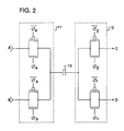
- FIG. 2 shows an exemplary embodiment of the switches 11, 12 and the capacitor 13.
- FIG. 3 diagrams the clock signals used to drive the transistors in FIG. 2 to implement the sequence described above.
- FIG. 2 An exemplary switch 11, 12 is shown in FIG. 2. Pairs of transistors (not numbered), one an N-channel and the other a P-channel FET for CMOS implementations, make the connection between the common and the two contacts of each switch 11, 12 (A, B and C, D, respectively). The transistors in each pair are driven by corresponding ones of oppositely phased clock signal pairs ⁇ 1, ⁇ 1 - ⁇ 4, ⁇ 4. The pairs of transistors provide a low impedance path for signals coupled thereby. For typical NMOS or PMOS implementations, a single transistor is used as a switch.
- FIG. 3 representative clock signals of the pairs of clock signals ⁇ 1 , ⁇ 1 - ⁇ 4, ⁇ 4 are shown for the four states of the circuit 10 (FIG. 1), corresponding to the figures FIG. 1a - 1d.
- FIG. 1 For clarity, only the positive clock signals (those coupling to the N-channel transistors in FIG. 2) are shown; when a clock signal is "high”, the corresponding transistor pair in the switches 11, 12 (FIG. 2) are “on” or conducting. Conversely, when the clock signal is "low”, the corresponding transistor pair is "off' or non-conducting.
- the four states are exaggerated (not to scale) to make the operation of the switches 11, 12 more clear. For simplicity, the non-overlapping clock aspect to ensure the break-before-make action of the switches 11, 12, described above, has been removed.
- the clock signals ⁇ 1 - ⁇ 4 are shown to have the initial state of switch 11 (FIG. 2) coupling the common thereof to contact B and the common of switch 12 (FIG. 2) coupling to contact D.
- the switch 12 operates and changes contacts from D to C.
- the switch 11 operates to change contacts from B to A, corresponding to FIG. 1c.
- the circuit 10 (FIG. 1) remains in this state for a relatively long period to ensure the voltages in the circuit 10 have stabilized.
- the switch 12 again operates to change contacts from C back to D, as shown in FIG. 1d. Soon thereafter, the switch 11 operates, changing contacts back to B, as shown in FIG. 1a.
- S-C circuit 10 described above is shown having only one amplifier 16 with a virtual ground input, another amplifier having a virtual ground input may be substituted for the ground connection to contact D of switch 11. Further, the circuit may implemented in fully differential form, with the circuits duplicated and operating in parallel.
Landscapes
- Engineering & Computer Science (AREA)
- Power Engineering (AREA)
- Filters That Use Time-Delay Elements (AREA)
- Keying Circuit Devices (AREA)
- Electronic Switches (AREA)
Applications Claiming Priority (2)
| Application Number | Priority Date | Filing Date | Title |
|---|---|---|---|
| US07/471,170 US5039963A (en) | 1990-01-26 | 1990-01-26 | Method for reducing signal-dependent distortion in switched-capacitor filters or the like |
| US471170 | 1990-01-26 |
Publications (2)
| Publication Number | Publication Date |
|---|---|
| EP0439276A2 true EP0439276A2 (de) | 1991-07-31 |
| EP0439276A3 EP0439276A3 (en) | 1992-01-15 |
Family
ID=23870531
Family Applications (1)
| Application Number | Title | Priority Date | Filing Date |
|---|---|---|---|
| EP19910300351 Withdrawn EP0439276A3 (en) | 1990-01-26 | 1991-01-17 | Method for reducing signal-dependent distortion in switched-capacitor filters or the like |
Country Status (3)
| Country | Link |
|---|---|
| US (1) | US5039963A (de) |
| EP (1) | EP0439276A3 (de) |
| JP (1) | JPH057131A (de) |
Cited By (1)
| Publication number | Priority date | Publication date | Assignee | Title |
|---|---|---|---|---|
| EP0678980A1 (de) * | 1994-04-21 | 1995-10-25 | STMicroelectronics S.r.l. | Verzerrungsarme Schaltung mit geschalteten Kapazitäten |
Families Citing this family (9)
| Publication number | Priority date | Publication date | Assignee | Title |
|---|---|---|---|---|
| US4950120A (en) * | 1989-02-27 | 1990-08-21 | Burndy Corporation | Apparatus and method for feeding card edge connectors and connector magazines |
| JP3337241B2 (ja) * | 1991-07-26 | 2002-10-21 | テキサス インスツルメンツ インコーポレイテツド | 改良型多重チャンネル・センサーインターフェース回路とその製造方法 |
| FI93684C (fi) * | 1993-04-23 | 1995-05-10 | Nokia Mobile Phones Ltd | Menetelmä signaalin käsittelemiseksi ja menetelmän mukainen signaalinkäsittelypiiri |
| US5790064A (en) * | 1996-04-10 | 1998-08-04 | Oasis Design, Inc. | Apparatus and method for switching capacitors within a switched capacitor circuit at times selected to avoid data dependent loading upon reference voltage supplies |
| DE19630416C1 (de) | 1996-07-26 | 1997-10-23 | Sgs Thomson Microelectronics | SC-Filter mit intrinsischer Anti-Aliasing-Funktion sowie damit ausgerüsteter Audiosignalprocessor |
| JP4674976B2 (ja) * | 2001-01-29 | 2011-04-20 | ローム株式会社 | 音質調整装置 |
| US7513779B2 (en) * | 2003-06-04 | 2009-04-07 | Hewlett-Packard Development Company, L.P. | Connector having a bypass capacitor and method for reducing the impedance and length of a return-signal path |
| US7147514B2 (en) * | 2004-02-05 | 2006-12-12 | Hewlett-Packard Development Company, L.P. | Connector providing capacitive coupling |
| US8810975B2 (en) * | 2010-07-17 | 2014-08-19 | Lsi Corporation | Input capacitor protection circuit |
Family Cites Families (12)
| Publication number | Priority date | Publication date | Assignee | Title |
|---|---|---|---|---|
| US4313096A (en) * | 1979-11-19 | 1982-01-26 | Bell Telephone Laboratories, Incorporated | Parasitic-free switched capacitor network |
| US4315227A (en) * | 1979-12-05 | 1982-02-09 | Bell Telephone Laboratories, Incorporated | Generalized switched-capacitor active filter |
| US4574250A (en) * | 1981-10-13 | 1986-03-04 | Intel Corporation | Switched capacitor filter utilizing a differential input and output circuit and method |
| JPS58125909A (ja) * | 1982-01-21 | 1983-07-27 | Nec Corp | スイツチドキヤパシタフイルタ |
| US4531106A (en) * | 1983-10-04 | 1985-07-23 | At&T Technologies, Inc. | Switched capacitor circuits |
| JPS60140478A (ja) * | 1983-12-27 | 1985-07-25 | Toshiba Corp | スイツチド・キヤパシタ積分器 |
| US4716388A (en) * | 1984-12-24 | 1987-12-29 | Jacobs Gordon M | Multiple output allpass switched capacitor filters |
| JPS62291214A (ja) * | 1986-06-11 | 1987-12-18 | Hitachi Ltd | スイツチドキヤパシタフイルタ |
| JP2592449B2 (ja) * | 1987-02-27 | 1997-03-19 | 株式会社日立製作所 | 波形等化器 |
| IT1215374B (it) * | 1987-03-05 | 1990-02-08 | Sgs Microelettronica Spa | Filtro elettronico integrato attivo avente bassissima sensitivita' alle ariazioni dei componenti. |
| JPS6449311A (en) * | 1987-08-19 | 1989-02-23 | Fujitsu Ltd | Clock generating circuit for switched capacitor filter |
| US4857860A (en) * | 1988-06-06 | 1989-08-15 | Linear Technology Corporation | Clock-sweepable low-pass filter having DC gain accuracy and reduced DC offset |
-
1990
- 1990-01-26 US US07/471,170 patent/US5039963A/en not_active Expired - Fee Related
-
1991
- 1991-01-17 EP EP19910300351 patent/EP0439276A3/en not_active Withdrawn
- 1991-01-18 JP JP3016789A patent/JPH057131A/ja active Pending
Cited By (2)
| Publication number | Priority date | Publication date | Assignee | Title |
|---|---|---|---|---|
| EP0678980A1 (de) * | 1994-04-21 | 1995-10-25 | STMicroelectronics S.r.l. | Verzerrungsarme Schaltung mit geschalteten Kapazitäten |
| US6556072B1 (en) | 1994-04-21 | 2003-04-29 | Stmicroelectronics S.R.L. | Low distortion circuit with switched capacitors |
Also Published As
| Publication number | Publication date |
|---|---|
| EP0439276A3 (en) | 1992-01-15 |
| JPH057131A (ja) | 1993-01-14 |
| US5039963A (en) | 1991-08-13 |
Similar Documents
| Publication | Publication Date | Title |
|---|---|---|
| EP0060026B1 (de) | Verstärkerstufe mit Operationsverstärker und äquivalentem Widerstandsschaltkreis mit schaltbaren Kapazitäten | |
| US4857778A (en) | Programmable universal active filter | |
| US4683386A (en) | Electronic attenuation value control circuit in which switching noise is suppressed | |
| US20020113724A1 (en) | Code independent charge transfer scheme for switched-capacitor digital-to-analog converter | |
| EP0689286B1 (de) | Schaltung mit getakteten Kapazitäten mit niedriger Versorgungsspannung unter Verwendung von getakteten Operationsverstärkern mit optimiertem Spannungshub | |
| US5391999A (en) | Glitchless switched-capacitor biquad low pass filter | |
| US5617055A (en) | Electronic switch having reduced body effect | |
| US4531106A (en) | Switched capacitor circuits | |
| EP0401552A3 (de) | Differentialer Kipposzillator | |
| JPH0468668B2 (de) | ||
| KR100291879B1 (ko) | 신호입력회로 | |
| EP0439276A2 (de) | Reduktionsverfahren für signalabhängige Verzerrungen in Filtern mit geschalteten Kapazitäten oder dergleichen | |
| JPH09181588A (ja) | 半導体スイッチ | |
| EP1252633A1 (de) | Geschulterter operationsverstärker- verfahren für schaltungen mit geschalteter kapazität unter niedriger spannung | |
| US4746871A (en) | Differential switched capacitor integrator using a single integration capacitor | |
| US20050017793A1 (en) | Boosted sampling circuit and relative method of driving | |
| EP0678980B1 (de) | Verzerrungsarme Schaltung mit geschalteten Kapazitäten | |
| EP1383241A1 (de) | Geschaltete Pegelschiebeschaltung in einem Analogschalter | |
| US5973537A (en) | Common mode control circuit for a switchable fully differential Op-AMP | |
| US4647865A (en) | Parasitic insensitive switched capacitor input structure for a fully differential operational amplifier | |
| US5528179A (en) | Constant capacitance prgrammable transconductance input stage | |
| US20030098722A1 (en) | Low charge-dump transistor switch | |
| GB2299472A (en) | Switched capacitor differential circuits with spike immunity | |
| EP0312142B1 (de) | Ausleseschaltung einer Verzögerungsschaltung | |
| GB2158666A (en) | Improvements in or relating to noise suppression interface circuits |
Legal Events
| Date | Code | Title | Description |
|---|---|---|---|
| PUAI | Public reference made under article 153(3) epc to a published international application that has entered the european phase |
Free format text: ORIGINAL CODE: 0009012 |
|
| AK | Designated contracting states |
Kind code of ref document: A2 Designated state(s): DE FR GB |
|
| PUAL | Search report despatched |
Free format text: ORIGINAL CODE: 0009013 |
|
| AK | Designated contracting states |
Kind code of ref document: A3 Designated state(s): DE FR GB |
|
| 17P | Request for examination filed |
Effective date: 19920701 |
|
| RAP3 | Party data changed (applicant data changed or rights of an application transferred) |
Owner name: AT&T CORP. |
|
| 17Q | First examination report despatched |
Effective date: 19941222 |
|
| STAA | Information on the status of an ep patent application or granted ep patent |
Free format text: STATUS: THE APPLICATION HAS BEEN WITHDRAWN |
|
| 18W | Application withdrawn |
Withdrawal date: 19950310 |