EP0439922A2 - Système de test de circuit integré utilisant des transistors latéraux - Google Patents
Système de test de circuit integré utilisant des transistors latéraux Download PDFInfo
- Publication number
- EP0439922A2 EP0439922A2 EP90312894A EP90312894A EP0439922A2 EP 0439922 A2 EP0439922 A2 EP 0439922A2 EP 90312894 A EP90312894 A EP 90312894A EP 90312894 A EP90312894 A EP 90312894A EP 0439922 A2 EP0439922 A2 EP 0439922A2
- Authority
- EP
- European Patent Office
- Prior art keywords
- pin
- current
- pins
- connector
- conductor means
- Prior art date
- Legal status (The legal status is an assumption and is not a legal conclusion. Google has not performed a legal analysis and makes no representation as to the accuracy of the status listed.)
- Granted
Links
Images


Classifications
-
- G—PHYSICS
- G01—MEASURING; TESTING
- G01R—MEASURING ELECTRIC VARIABLES; MEASURING MAGNETIC VARIABLES
- G01R31/00—Arrangements for testing electric properties; Arrangements for locating electric faults; Arrangements for electrical testing characterised by what is being tested not provided for elsewhere
- G01R31/28—Testing of electronic circuits, e.g. by signal tracer
- G01R31/2801—Testing of printed circuits, backplanes, motherboards, hybrid circuits or carriers for multichip packages [MCP]
- G01R31/281—Specific types of tests or tests for a specific type of fault, e.g. thermal mapping, shorts testing
- G01R31/2813—Checking the presence, location, orientation or value, e.g. resistance, of components or conductors
Definitions
- This invention relates to measuring and testing devices and more particularly to in-circuit testing devices. Even more particularly, the invention relates to in-circuit testing of connections between an integrated circuit and a printed circuit board.
- Functional testing uses a procedure of applying predetermined input signals and monitoring the output of a printed circuit board to determine if all of the components are present and operating properly on the circuit board. While functional testing provides a way of determining whether the P.C. board is functioning properly, it provides little or no information regarding the functioning of individual components on the board. Complex programming techniques have been used to provide limited information as to the location of non-functioning components on the board by carefully selecting input data and analyzing the output results. Such systems are complex, often costly to implement, and normally provide only vague information as to the location of malfunctioning components.
- in-circuit testing techniques have been used to individually test the components on the printed circuit board to determine if these components are working properly.
- This process uses a "bed of nails" tester to access each individual component and test that component individually. In this manner, non-functioning components can be identified and replaced to prevent the entire circuit board from being scrapped. This process works well for simple components where circuit inside the component is known and can be easily tested. If the component being tested is very complex, or if the circuit inside the component is unknown, in-circuit testing may not achieve satisfactory results.
- Manufacturing defect analyzers are another class of testing devices that provide simpler tests and are less expensive to implement. These devices are designed to locate manufacturing faults, such as shorts on a printed circuit board, missing integrated circuits, bent component pins, etc. Although these devices do a reasonably good job of finding shorts and gross analog faults, they are marginal when testing digital sections of the board.
- the device of U.S. Patent 4,779,041, issued October 18, 1988 to Williamson attempts to solve the above described problem.
- the device and test method of Williamson models a general circuit inside the device as a pair of diodes having a common resistor. This resistor is created by the wire between the device components and the external ground pin of the device. A current is passed through one of the diodes using a constant current source, to forward bias the diode. A large current pulse is then applied to the other of the diodes. The large current pulse will cause a voltage drop across the common resistor, and this voltage drop can be measured to determine whether all three pins are connected.
- the device of Williamson suffers some limitations.
- the common resistor Because the value of the common resistor is small, a large current pulse is needed to measure an appreciable voltage drop. Also, some current passes through adjacent devices connected to the pins, thus lowering the amount of current through the common resistor. In addition, if several pins are connected to ground in the device under test, the resistance of all these pins is placed in parallel with the common resistor, again reducing the amount of voltage which can be measured.
- Yet another object of the invention is to provide such an apparatus and method that is insensitive to fan out of the pin being tested.
- Still another object of the present invention is to provide such an apparatus and method that is insensitive to the number of ground pins of the component being tested.
- the above and other objects of the present invention are accomplished in a system that overcomes the disadvantages and limitations of the prior art by providing an apparatus and method for determining whether semiconductor components are present and properly connected to a printed circuit board.
- the present invention determines whether input and output connector pins, as well as a ground pin for bipolar semiconductor components and metal oxide semiconductor (MOS) components are conductively connected to a circuit on a printed circuit board, and whether proper conductive paths exist between the connector pins and the ground pin through the semiconductor.
- MOS metal oxide semiconductor
- the semiconductor material between two pins of an integrated circuit can be viewed as a lateral transistor, having its base connected directly to the semiconductor substrate pin of the component.
- the substrate is typically connected to the ground pin for digital components, and the most negative supply connection for analog components.
- a constant voltage source such as might be supplied by an op amp and feedback network, is applied to a first pin of the component being tested. After the circuit has had time to stabilize, the current flowing into this first pin is measured. A current source is then connected to a second pin of the device, typically an adjacent pin, and a current pulse is applied to this second pin.
- the first pin having the voltage source connected thereto, acts as a collector of the lateral transistor
- the second pin having the current source connected thereto, acts as an emitter to the lateral transistor. Therefore, when a current pulse is applied to the second pin, the current on the first pin is monitored and if a corresponding current pulse is detected on the first pin, the first and second pins as well as the ground pin of the component are properly connected to printed circuit board.
- the voltage applied to the first pin described above is provided by the inverting input to an op amp which has a feedback resistor connected from the output of the op amp to this same inverting input pin.
- the non-inverting input to the op amp is connected to a voltage source. Because of the nature of op amps, the inverting input will be maintained at the same voltage level as the non-inverting input. Therefore, this constant voltage will be supplied to the collector pin of the device under test.
- the current flowing into the pin of the device under test can be measured.
- the voltage across the feedback resistor of the op amp will indicate whether additional current flows into the device under test, and therefore whether the device under test is connected to the printed circuit board.
- a negative voltage source is applied to the second pin to cause the current flow from the emitter of the lateral transistor.
- the advantage of the present system is that it provides a simple and inexpensive system equivalent to a manufacturing defects analyzer for digital components such as TTL. It does not rely on the characteristics of the circuit within the device under test, and it is less sensitive than other methods to adjacent devices and to fan out of the pins in the device under test. This method is also less sensitive to the number of ground pins on the device under test than other methods.
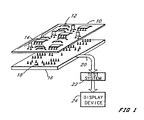
- Fig. 1 shows a schematic overall view of an implementation of the device of the present invention.
- printed circuit board 10 has a plurality of both analog and digital components 12 connected by way of the component leads through a plurality of conductors 14 that form a circuit on the printed circuit board 10.
- Test bed 16 has a plurality of connector pins 18 that function to contact conductors 14 at predetermined locations to apply test signals and detect responses at predetermined locations within printed circuit board 10.
- Conductors 20 connect the test bed pins 18 to test system 22.
- Test system 22 includes the necessary signal generators and signal processing equipment to perform the operations and analysis of the present invention and provide a display for display device 24 to indicate any defects that may exist in the circuit of printed circuit board 10.
- Fig. 2 shows a partial schematic diagram of a typical prior art Schottky TTL circuit within an integrated circuit component.
- the circuit illustrated in Fig. 2 can be implemented in TTL or MOS components, such as complimentary metal oxide semiconductors (CMOS).
- CMOS complimentary metal oxide semiconductors
- the circuit illustrated in Fig. 2 may be implemented slightly differently in CMOS circuitry and may function slightly differently, the overall configuration and overall functional capabilities are generally similar to TTL implementation.
- the present invention may be implemented with slight variations for use with CMOS components.
- the input 26 of the TTL circuit of Fig. 2 is connected to transistor 28 and protection diode 30.
- Resistor 32 is coupled to VCC input 34 and the base lead of transistor 28.
- Output 36 is connected to the collector of transistor 40.
- Fig. 3 shows a cross-sectional view of two of the components of Fig. 2.
- dashed line 42 surrounds an area that forms the transistor 28 and protection diode 30 of Fig. 2.
- dashed line 44 surrounds an area that forms the transistor 40 of Fig. 2.
- a parasitic lateral NPN transistor is formed by the cathode 46 of the protection diode 30, which can act either as a collector or an emitter, the substrate 48, which acts as a base, and the collector 50 of the output transistor 40, which acts as a collector or emitter.
- the parasitic lateral transistor thus formed has very poor characteristics, with a beta of typically 0.01, it is capable of serving the testing function of the present invention. Many different lateral transistors are formed in this manner on every integrated circuit, thus the present invention can be used to test for connections to most of the input and output pins of an integrated circuit.
- Fig. 4 shows a schematic diagram of the present invention.
- an integrated circuit device under test (DUT) 100 has a ground pin 102 and pair of test pins 104 and 106. Each of the pins 102, 104, and 106 can be connected to multiple pins of an integrated circuit.
- An op amp 108 has its non-inverting input 110 connected to a battery or other constant voltage source 112 to supply a constant voltage to the non-inverting input 110.
- a feedback resistor 114 is connected between the output 116 of the op amp and the inverting input 118 of the op amp.
- the inverting input 118 is also connected to test pin 106 of the device under test 100.
- the other pin 104 of the device under test is connected to a current source 120.
- the op amp 108 will cause the inverting input 118 to maintain the same voltage as the non-inverting input 110.
- the voltage must be sufficient to reverse bias the collector-base junction of the lateral transistor, and is typically 0.2 volts.
- test pin 106 will rise to the voltage of the inverting input 118 of the op amp 108, and the amount of current flowing into the device under test 100 through pin 106 can be measured by measuring the voltage across feedback resistor 114 at the output terminals 122 and 124.
- a current pulse is supplied to pin 104 by current source 120.
- Output terminals 122 and 124 are monitored while the current pulse is being applied to pin 104, and if a current pulse is also seen through resistor 114 as measured by the voltage on the output terminals 122 and 124, then pins 106, 104, and 102 must all be connected to the printed circuit board.
- the pins 104 and 106 on the device under test 100 will be adjacent each other, however, the system will work so long as both these pins are connected to the same substrate within the integrated circuit. Should the integrated circuit being tested contain multiple substrates, and should the pins being tested be located on different substrates, then there will be no lateral transistor formed within the substrate and the system will not work properly. Because the lateral transistor 100 is not intentionally formed in the device under test, but is formed by a protection diode and a parasitic diode, the system does not rely on the actual circuit contained within the device under test. Because the current being measured across the feedback resistor 114 does not pass through the ground pin 102, the number of actual ground pins present in the device under test 100 does not substantially affect the operation of the system. Also, because the current is restricted to that flowing through the lateral transistor between pins 104 and 106, the fan out of the internal circuit has very little effect on the operation of the system.
- an additional regulated power supply must be connected between VCC and ground of the device under test. This supply is typically set to -0.3 volts for proper operation of the circuit.
- current source 120 is replaced by a negative voltage source. This negative voltage source serves to supply the current pulse through the NPN lateral transistor.
- Fig. 5 shows a flowchart of the operation of the present invention.
- block 150 selects the pins to be tested on the device under test.
- Block 152 then connects the op amp circuit and the current source to the device under test, and block 154 delays approximately 10 microseconds to allow the op amp circuit and the parasitic lateral transistor to stabilize.
- block 156 measures the current going into the lateral transistor DUT by measuring the voltage across resistor 114 (Fig. 2).
- Block 158 then applies a current pulse, typically 20 milliamps, or a voltage pulse, typically -1.5 volts, to the emitter pin of the device under test.
- Block 160 then measures the current going through the DUT by measuring the voltage across resistor 114, and block 162 compares the current value measured during the application of the current or voltage pulse, to the current value measured while the circuit was stabilized. If these two currents are equal, block 164 transfers to block 166 to display an error message to indicate that the device under test is not connected to the printed circuit board. If the currents are not equal, meaning that the current or voltage source 120 caused additional current to flow into the lateral transistor through pin 106, then the device under test is connected and block 164 simply returns to complete the test.
Landscapes
- Engineering & Computer Science (AREA)
- Computer Hardware Design (AREA)
- Microelectronics & Electronic Packaging (AREA)
- General Engineering & Computer Science (AREA)
- Physics & Mathematics (AREA)
- General Physics & Mathematics (AREA)
- Tests Of Electronic Circuits (AREA)
- Testing Of Short-Circuits, Discontinuities, Leakage, Or Incorrect Line Connections (AREA)
Applications Claiming Priority (2)
| Application Number | Priority Date | Filing Date | Title |
|---|---|---|---|
| US472926 | 1983-03-07 | ||
| US07/472,926 US5101152A (en) | 1990-01-31 | 1990-01-31 | Integrated circuit transfer test device system utilizing lateral transistors |
Publications (3)
| Publication Number | Publication Date |
|---|---|
| EP0439922A2 true EP0439922A2 (fr) | 1991-08-07 |
| EP0439922A3 EP0439922A3 (en) | 1992-04-29 |
| EP0439922B1 EP0439922B1 (fr) | 1995-07-19 |
Family
ID=23877458
Family Applications (1)
| Application Number | Title | Priority Date | Filing Date |
|---|---|---|---|
| EP90312894A Expired - Lifetime EP0439922B1 (fr) | 1990-01-31 | 1990-11-27 | Système de test de circuit integré utilisant des transistors latéraux |
Country Status (4)
| Country | Link |
|---|---|
| US (1) | US5101152A (fr) |
| EP (1) | EP0439922B1 (fr) |
| JP (1) | JP3195800B2 (fr) |
| DE (1) | DE69021036T2 (fr) |
Cited By (2)
| Publication number | Priority date | Publication date | Assignee | Title |
|---|---|---|---|---|
| EP0571963A3 (fr) * | 1992-05-29 | 1994-04-13 | Spea Srl | |
| DE19733113A1 (de) * | 1997-07-31 | 1999-02-18 | Oce Printing Systems Gmbh | Verfahren zum Testen einer elektronischen Baugruppe und elektronische Baugruppe mit Testhilfe |
Families Citing this family (10)
| Publication number | Priority date | Publication date | Assignee | Title |
|---|---|---|---|---|
| US5557209A (en) * | 1990-12-20 | 1996-09-17 | Hewlett-Packard Company | Identification of pin-open faults by capacitive coupling through the integrated circuit package |
| US5625292A (en) * | 1990-12-20 | 1997-04-29 | Hewlett-Packard Company | System for measuring the integrity of an electrical contact |
| DE4110551C1 (fr) * | 1991-03-30 | 1992-07-23 | Ita Ingenieurbuero Fuer Testaufgaben Gmbh, 2000 Hamburg, De | |
| US5225816A (en) * | 1991-08-12 | 1993-07-06 | Motorola, Inc. | Electrical connector with display |
| US5420500A (en) * | 1992-11-25 | 1995-05-30 | Hewlett-Packard Company | Pacitive electrode system for detecting open solder joints in printed circuit assemblies |
| US5818251A (en) * | 1996-06-11 | 1998-10-06 | National Semiconductor Corporation | Apparatus and method for testing the connections between an integrated circuit and a printed circuit board |
| JP4174167B2 (ja) * | 2000-04-04 | 2008-10-29 | 株式会社アドバンテスト | 半導体集積回路の故障解析方法および故障解析装置 |
| EP2007219A1 (fr) | 2006-03-13 | 2008-12-31 | NATURIN GmbH & CO. | Compositions thermodurcissables a base de proteines biodegradables, procedes de preparation et applications |
| ES2641583T3 (es) | 2007-04-16 | 2017-11-10 | Marquardt Gmbh | Procedimiento para la fabricación de un interruptor electromecánico |
| CN113009266B (zh) * | 2021-03-18 | 2024-06-21 | 广州亚美智造科技有限公司 | 一种治具插拔检测电路 |
Family Cites Families (14)
| Publication number | Priority date | Publication date | Assignee | Title |
|---|---|---|---|---|
| US3335340A (en) * | 1964-02-24 | 1967-08-08 | Ibm | Combined transistor and testing structures and fabrication thereof |
| US3622883A (en) * | 1965-08-18 | 1971-11-23 | Ibm | Pulsed current transistor beta tester having feedback to maintain emitter to collector current constant |
| US3774088A (en) * | 1972-12-29 | 1973-11-20 | Ibm | An integrated circuit test transistor structure and method of fabricating the same |
| CA997481A (en) * | 1972-12-29 | 1976-09-21 | International Business Machines Corporation | Dc testing of integrated circuits and a novel integrated circuit structure to facilitate such testing |
| US3889188A (en) * | 1973-07-30 | 1975-06-10 | Ibm | Time zero determination of FET reliability |
| US4042832A (en) * | 1975-12-29 | 1977-08-16 | Honeywell Information Systems Inc. | Logic board interlock indication apparatus |
| DE2840981C2 (de) * | 1977-10-08 | 1984-03-29 | Tokyo Electric Co., Ltd., Tokyo | Speichereinsatz für elektronische Registrierkassen und Datenverarbeitungseinheiten |
| EP0075079A1 (fr) * | 1981-09-21 | 1983-03-30 | International Business Machines Corporation | Système pour contrôler le réseau d'un circuit |
| GB8428405D0 (en) * | 1984-11-09 | 1984-12-19 | Membrain Ltd | Automatic test equipment |
| US4864219A (en) * | 1987-03-19 | 1989-09-05 | Genrad, Inc. | Method and apparatus for verifying proper placement of integrated circuits on circuit boards |
| US4779041A (en) * | 1987-05-20 | 1988-10-18 | Hewlett-Packard Company | Integrated circuit transfer test device system |
| US4801878A (en) * | 1987-06-18 | 1989-01-31 | Hewlett-Packard Company | In-circuit transistor beta test and method |
| US4894605A (en) * | 1988-02-24 | 1990-01-16 | Digital Equipment Corporation | Method and on-chip apparatus for continuity testing |
| US4896108A (en) * | 1988-07-25 | 1990-01-23 | American Telephone And Telegraph Company, At&T Bell Laboratories | Test circuit for measuring specific contact resistivity of self-aligned contacts in integrated circuits |
-
1990
- 1990-01-31 US US07/472,926 patent/US5101152A/en not_active Expired - Lifetime
- 1990-11-27 DE DE69021036T patent/DE69021036T2/de not_active Expired - Fee Related
- 1990-11-27 EP EP90312894A patent/EP0439922B1/fr not_active Expired - Lifetime
-
1991
- 1991-01-31 JP JP03201191A patent/JP3195800B2/ja not_active Expired - Fee Related
Cited By (3)
| Publication number | Priority date | Publication date | Assignee | Title |
|---|---|---|---|---|
| EP0571963A3 (fr) * | 1992-05-29 | 1994-04-13 | Spea Srl | |
| DE19733113A1 (de) * | 1997-07-31 | 1999-02-18 | Oce Printing Systems Gmbh | Verfahren zum Testen einer elektronischen Baugruppe und elektronische Baugruppe mit Testhilfe |
| DE19733113B4 (de) * | 1997-07-31 | 2008-01-31 | OCé PRINTING SYSTEMS GMBH | Verfahren zum Testen einer elektronischen Baugruppe und elektronische Baugruppe mit Testhilfe |
Also Published As
| Publication number | Publication date |
|---|---|
| JP3195800B2 (ja) | 2001-08-06 |
| DE69021036D1 (de) | 1995-08-24 |
| JPH04213077A (ja) | 1992-08-04 |
| US5101152A (en) | 1992-03-31 |
| DE69021036T2 (de) | 1995-11-30 |
| EP0439922A3 (en) | 1992-04-29 |
| EP0439922B1 (fr) | 1995-07-19 |
Similar Documents
| Publication | Publication Date | Title |
|---|---|---|
| US4779041A (en) | Integrated circuit transfer test device system | |
| US5818251A (en) | Apparatus and method for testing the connections between an integrated circuit and a printed circuit board | |
| JP2664429B2 (ja) | 回路板検査装置および方法 | |
| US6828815B2 (en) | Method and apparatus for defect analysis of semiconductor integrated circuit | |
| US5726997A (en) | Apparatus and method for testing of integrated circuits | |
| US5280237A (en) | Method for testing semiconductor integrated circuits soldered to boards and use of a transistor tester for this method | |
| JP3816975B2 (ja) | 製造欠陥分析装置 | |
| EP0439922B1 (fr) | Système de test de circuit integré utilisant des transistors latéraux | |
| JPH06160457A (ja) | 回路板試験装置 | |
| US5933309A (en) | Apparatus and method for monitoring the effects of contact resistance | |
| JP3132927B2 (ja) | 半導体チップの検査方法 | |
| GB2387445A (en) | Measuring junction leakage in a semiconductor device | |
| US20120038367A1 (en) | Connection quality verification for integrated circuit test | |
| JPS6371669A (ja) | 電子回路装置の検査方法 | |
| JP2919312B2 (ja) | 半導体装置の検査方法 | |
| JPH06160487A (ja) | Cmos型集積回路のテストパターンおよび試験方法,テストパターンの作成方法 | |
| JPH0658989A (ja) | 配線基板のショート検出試験方法 | |
| JPH0541419A (ja) | 検査装置の評価方法 | |
| US20070229106A1 (en) | Measuring and identifying analog characteristics of a microelectronic component at a wafer level and a platform level | |
| JPH07191079A (ja) | 半導体集積回路の評価方法及び評価治具 | |
| JPH06230031A (ja) | プロ−ブカ−ドを用いた半導体素子の特性測定方法 | |
| Quah et al. | A study of integrated circuit IV characteristics using a fault localization system [FLS] | |
| JPH0652291B2 (ja) | 実装基板上のic部品の端子挿入状態判定方法 | |
| JPH08105933A (ja) | 半導体装置の試験方法 | |
| JP2000124273A (ja) | 半導体集積回路及びその電気的特性検査方法 |
Legal Events
| Date | Code | Title | Description |
|---|---|---|---|
| PUAI | Public reference made under article 153(3) epc to a published international application that has entered the european phase |
Free format text: ORIGINAL CODE: 0009012 |
|
| AK | Designated contracting states |
Kind code of ref document: A2 Designated state(s): DE FR GB |
|
| PUAL | Search report despatched |
Free format text: ORIGINAL CODE: 0009013 |
|
| AK | Designated contracting states |
Kind code of ref document: A3 Designated state(s): DE FR GB |
|
| 17P | Request for examination filed |
Effective date: 19921006 |
|
| 17Q | First examination report despatched |
Effective date: 19940414 |
|
| GRAA | (expected) grant |
Free format text: ORIGINAL CODE: 0009210 |
|
| AK | Designated contracting states |
Kind code of ref document: B1 Designated state(s): DE FR GB |
|
| REF | Corresponds to: |
Ref document number: 69021036 Country of ref document: DE Date of ref document: 19950824 |
|
| ET | Fr: translation filed | ||
| PLBE | No opposition filed within time limit |
Free format text: ORIGINAL CODE: 0009261 |
|
| STAA | Information on the status of an ep patent application or granted ep patent |
Free format text: STATUS: NO OPPOSITION FILED WITHIN TIME LIMIT |
|
| 26N | No opposition filed | ||
| REG | Reference to a national code |
Ref country code: GB Ref legal event code: 732E |
|
| REG | Reference to a national code |
Ref country code: GB Ref legal event code: 732E |
|
| REG | Reference to a national code |
Ref country code: FR Ref legal event code: TP |
|
| REG | Reference to a national code |
Ref country code: FR Ref legal event code: TP |
|
| REG | Reference to a national code |
Ref country code: GB Ref legal event code: IF02 |
|
| PGFP | Annual fee paid to national office [announced via postgrant information from national office to epo] |
Ref country code: FR Payment date: 20021030 Year of fee payment: 13 |
|
| PGFP | Annual fee paid to national office [announced via postgrant information from national office to epo] |
Ref country code: GB Payment date: 20021120 Year of fee payment: 13 |
|
| PG25 | Lapsed in a contracting state [announced via postgrant information from national office to epo] |
Ref country code: GB Free format text: LAPSE BECAUSE OF NON-PAYMENT OF DUE FEES Effective date: 20031127 |
|
| GBPC | Gb: european patent ceased through non-payment of renewal fee |
Effective date: 20031127 |
|
| PG25 | Lapsed in a contracting state [announced via postgrant information from national office to epo] |
Ref country code: FR Free format text: LAPSE BECAUSE OF NON-PAYMENT OF DUE FEES Effective date: 20040730 |
|
| REG | Reference to a national code |
Ref country code: FR Ref legal event code: ST |
|
| PGFP | Annual fee paid to national office [announced via postgrant information from national office to epo] |
Ref country code: DE Payment date: 20060102 Year of fee payment: 16 |
|
| PG25 | Lapsed in a contracting state [announced via postgrant information from national office to epo] |
Ref country code: DE Free format text: LAPSE BECAUSE OF NON-PAYMENT OF DUE FEES Effective date: 20070601 |