EP0440087A2 - Optical signal connecting device for plugs of a plug cabinet - Google Patents
Optical signal connecting device for plugs of a plug cabinet Download PDFInfo
- Publication number
- EP0440087A2 EP0440087A2 EP19910100887 EP91100887A EP0440087A2 EP 0440087 A2 EP0440087 A2 EP 0440087A2 EP 19910100887 EP19910100887 EP 19910100887 EP 91100887 A EP91100887 A EP 91100887A EP 0440087 A2 EP0440087 A2 EP 0440087A2
- Authority
- EP
- European Patent Office
- Prior art keywords
- connecting device
- inserts
- optical waveguide
- signal connecting
- optical
- Prior art date
- Legal status (The legal status is an assumption and is not a legal conclusion. Google has not performed a legal analysis and makes no representation as to the accuracy of the status listed.)
- Granted
Links
- 230000003287 optical effect Effects 0.000 title claims abstract description 47
- 230000008878 coupling Effects 0.000 claims abstract description 22
- 238000010168 coupling process Methods 0.000 claims abstract description 22
- 238000005859 coupling reaction Methods 0.000 claims abstract description 22
- 238000003384 imaging method Methods 0.000 claims abstract description 13
- 238000004891 communication Methods 0.000 claims abstract description 9
- 239000000835 fiber Substances 0.000 claims abstract description 3
- 239000013307 optical fiber Substances 0.000 claims description 7
- 239000004020 conductor Substances 0.000 claims description 4
- 230000002457 bidirectional effect Effects 0.000 claims description 3
- 230000001419 dependent effect Effects 0.000 claims 1
- 230000005540 biological transmission Effects 0.000 abstract description 3
- RYGMFSIKBFXOCR-UHFFFAOYSA-N Copper Chemical compound [Cu] RYGMFSIKBFXOCR-UHFFFAOYSA-N 0.000 description 2
- 230000000712 assembly Effects 0.000 description 2
- 238000000429 assembly Methods 0.000 description 2
- 229910052802 copper Inorganic materials 0.000 description 2
- 239000010949 copper Substances 0.000 description 2
- 238000010276 construction Methods 0.000 description 1
- 238000004870 electrical engineering Methods 0.000 description 1
- 238000000034 method Methods 0.000 description 1
- 238000000926 separation method Methods 0.000 description 1
- 238000007493 shaping process Methods 0.000 description 1
- 230000008054 signal transmission Effects 0.000 description 1
Images


Classifications
-
- G—PHYSICS
- G02—OPTICS
- G02B—OPTICAL ELEMENTS, SYSTEMS OR APPARATUS
- G02B6/00—Light guides; Structural details of arrangements comprising light guides and other optical elements, e.g. couplings
- G02B6/24—Coupling light guides
- G02B6/42—Coupling light guides with opto-electronic elements
- G02B6/43—Arrangements comprising a plurality of opto-electronic elements and associated optical interconnections
-
- G—PHYSICS
- G02—OPTICS
- G02B—OPTICAL ELEMENTS, SYSTEMS OR APPARATUS
- G02B6/00—Light guides; Structural details of arrangements comprising light guides and other optical elements, e.g. couplings
- G02B6/24—Coupling light guides
- G02B6/26—Optical coupling means
- G02B6/34—Optical coupling means utilising prism or grating
-
- G—PHYSICS
- G02—OPTICS
- G02B—OPTICAL ELEMENTS, SYSTEMS OR APPARATUS
- G02B6/00—Light guides; Structural details of arrangements comprising light guides and other optical elements, e.g. couplings
- G02B6/24—Coupling light guides
- G02B6/42—Coupling light guides with opto-electronic elements
- G02B6/4201—Packages, e.g. shape, construction, internal or external details
- G02B6/4246—Bidirectionally operating package structures
Definitions
- the invention relates to a signal connection device for establishing communication paths between inserts of a rack.
- the invention is therefore based on the object of providing a signal connection device for creating communication paths between inserts of a slide-in rack, which is of a very simple construction and is nevertheless suitable for the highest signal speeds.
- each signal connection is formed by an optical waveguide which is assigned to a rear wall of the frame, the coupling being effected by means of a counter-position or system in the inserted position from imaging optics of the slots to the optical waveguide of the rear wall.
- the use of optical signal paths allows the highest signal transmission speeds. Nevertheless, the effort of this optical communication remains very low, since a back wall provided with optical fibers is used.
- a corresponding imaging optics of the slide-in module are operatively connected to the optical waveguide arranged in the rear wall, so that an optical signal can be coupled in or out.
- This coupling or decoupling takes place only by juxtaposing or placing the imaging optics of the plug-in to or on the optical waveguide of the rear wall.
- the optical waveguide is arranged on or in a carrier film which is located on a carrier of the rear wall.
- the back wall therefore consists of several "layers".
- it has a carrier on which a carrier film is applied, with which the optical waveguide, which is correspondingly thin for high-frequency transmission, can be handled.
- the optical waveguide can be applied to the surface of the carrier film or embedded therein.
- the imaging optics are placed opposite to the optical waveguide, so that, for example, an optical signal supplied by a laser diode is coupled into the optical waveguide via the imaging optics, and at one at another point - decoupled from the optical waveguide, passed through an imaging optic of another insert and, for example, fed to a photodiode of this insert.
- the optical waveguide is formed over the entire surface on or in the carrier film, which covers the entire surface of the plate-shaped carrier.
- the carrier film provided with optical waveguides it is also possible for the carrier film provided with optical waveguides to cover only certain subareas of the carrier.
- This full-surface or partial-surface configuration enables the coupling or uncoupling at different points on the optical waveguide, since this represents a flat structure.
- a multipoint-to-point connection or a multipoint-to-multipoint connection is also conceivable.
- the optical waveguide is designed as a strip on or in the carrier film.
- a point-to-point connection can be established, that is to say a concrete connection from a certain insert to another insert. If several inserts are to be connected to one another, several optical waveguides designed as strips can be assigned to the rear wall. It comes to it Intersections of the individual strip optical waveguides are formed in different layers of the carrier film.
- Openings can also be provided for receiving conductor tracks in the carrier film.
- the conductor tracks are arranged on the side of the carrier facing the inserts and are acted upon by spring contacts of the inserts. This allows e.g. lead the supply voltage to the individual modules.
- communication paths designed in this way are also possible, which exist in addition to the optical signal connections according to the invention.
- a coupling structure is formed in the film or in the optical waveguide at the coupling-in and coupling-out points.
- the coupling structure enables the transmission light to be coupled into the optical waveguide or the light to be coupled out in order to feed it to a receiving unit.
- the coupling structure can be formed, for example, by a grating, in particular a holographic grating. Furthermore, it is also possible to scratch the film only in the area of the coupling or decoupling point, which takes place when a plug-in is inserted for the first time at a suitable point — that is, in contrast to the imaging optics.
- a sine grid, a triangular grid or a sawtooth grid can be used as the grid.
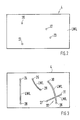
- FIG. 1 shows a schematic side view of two inserts 1 and 2, which are inserted into a frame (not shown).
- the two slots 1 and 2 are in the slot position.
- Inserts 1 and 2 have electronic circuits which e.g. belong to a broadband exchange.
- a signal connection device 3 is provided, by means of which communication paths between the inserts 1 and 2 are established.
- the broadband switching system can of course do more exist as only two inserts, but to illustrate the invention it is sufficient to only consider inserts 1 and 2.
- the signal connections of the communication paths between inserts 1 and 2 are designed as optical fibers.
- the rear wall 4 of the rack is included.
- the rear wall has a plate-shaped support 5, which forms a mechanical support.
- a support film 7 is applied over the entire surface and carries a flat optical waveguide LWL on its side 8 facing the inserts 1 and 2.
- optical waveguide LWL it is also possible for the optical waveguide LWL to be embedded in the carrier film 7.
- the insert 1 has a laser diode module.
- the light 10 generated by the laser diode module 9 is transmitted to an imaging optics 11, which is designed, for example, as a Selfoc lens.
- the bundled light 12 strikes the flat optical waveguide LWL at a coupling point 13 and is consequently transmitted up to a coupling point 14.
- the light 15 emanating from there is in turn bundled by means of imaging optics 16, the bundled light 17 being fed to a photodiode module 18. While the laser diode module 9 works as a transmitter, the photodiode module 18 represents a receiver.
- coupling structures 19 can be provided on the optical waveguide.
- an optical grating in particular a holographic grating, is formed there in each case.
- This grating can preferably be a sine grating, but according to a further exemplary embodiment also a triangular grating or else according to a further exemplary embodiment a sawtooth grating.
- the procedure is such that the periodicity of the grating (the distance between the individual columns of the grating) is matched to the wavelength of the light traveling in the optical waveguide.
- the respective grating it is also possible for the respective grating to have a different periodicity, that is to say, to have different distances between the individual columns, as viewed in terms of its spread.
- the aim is always for the light to be coupled into the optical waveguide with high efficiency and also to be coupled out with high efficiency. Since the shape and the direction of the light beam that is coupled in and out at the coupling point by means of the grating depends on the wavelength of the light, wavelength division multiplex connections are also possible. For example, two transmitters and two (or more) receivers on different wavelengths then work via an optical fiber (unidirectional operation). Furthermore, bidirectional operation is also possible, with two different wavelengths then Serve directional separation. There is then a transmitter and a receiver on each slot.
- FIG. 3 shows a further rear wall 4 which, compared to that of FIG. 2, does not have a full-surface optical waveguide, but a strip-shaped optical waveguide.
- coupling points 24, 25, 26 and 27 can be connected to coupling points 28, 29, 30 and 31, each of which, as already described in FIG. 1, lie opposite corresponding imaging optics of the associated plug-in units.
- the structure of the rear wall 4 in FIG. 3 corresponds to that in FIG Rear wall 4 housed so that there is no mutual interference.
- openings 33 can be formed in the carrier film, in which conductor tracks 34 are located. These are arranged on the side 6 of the carrier 5. They interact with spring contacts 35 of inserts 1 and 2 (not shown for insert 1). These measures make it possible to establish electrical connection paths between the inserts 1 and 2. Furthermore, these electrical contact connections can be used for supplying the supply voltage.
- wavelength multiplex connections are also possible.
- FIG. 4 For example, two laser diode modules 9a, 9b work as transmitters or receivers on different wavelengths via an optical waveguide (unidirectional operation). However, as already mentioned, bidirectional operation is also possible if the directions are separated by means of the different wavelengths. There is then a transmitter and a receiver on each slot.
- the imaging optics are identified by 11a and 11b.
- the light bears the reference numerals 10a, 10b or 12a and 12b.
- the lightwave multiplexer is an inherent part of the Fiber optic inputs and outputs are. This means that they are not part of interchangeable assemblies (inserts).
Landscapes
- Physics & Mathematics (AREA)
- General Physics & Mathematics (AREA)
- Optics & Photonics (AREA)
- Optical Couplings Of Light Guides (AREA)
- Optical Communication System (AREA)
- Optical Integrated Circuits (AREA)
- Mounting Of Printed Circuit Boards And The Like (AREA)
- Light Guides In General And Applications Therefor (AREA)
- Details Of Connecting Devices For Male And Female Coupling (AREA)
- Coupling Device And Connection With Printed Circuit (AREA)
- Mechanical Coupling Of Light Guides (AREA)
Abstract
Die Erfindung betrifft eine Signalverbindungsvorrichtung zur Herstellung von Kommunikationswegen zwischen Einschüben eines Einschubgestells. Für einen einfachen Aufbau bei großer Übertragungsgeschwindigkeit wird vorgeschlagen, daß jede Signalverbindung von einem Lichtwellenleiter (LWL) gebildet wird, der einer Rückwand (4) des Gestells zugeordnet ist, wobei die Kopplung durch in Einschubstellung erfolgende Gegenüberlage oder Anlage von Abbildungsoptiken (11,16) der Einschübe (1,2) zum Lichtwellenleiter (LWL) der Rückwand (4) erfolgt.
Description
Die Erfindung betrifft eine Signalverbindungsvorrichtung zur Erstellung von Kommunikationswegen zwischen Einschüben eines Einschubgestells.The invention relates to a signal connection device for establishing communication paths between inserts of a rack.
Auf vielen Gebieten der Elektrotechnik ist es üblich, einzelne Baugruppen oder Geräte als Einschübe zu erstellen, die in ein Einschubgestell eingebracht werden. Die einzelnen Einschübe sind über Kupfer-Koax-Kabel miteinander verbunden. Ein derartiger Aufbau ist beispielsweise in einem Breitband-Vermittlungssystem realisiert. Die geschilderte Gestellverkabelung ist sehr aufwendig.In many areas of electrical engineering, it is common to create individual assemblies or devices as plug-in modules that are inserted into a rack. The individual inserts are connected to each other via copper coax cables. Such a structure is implemented, for example, in a broadband switching system. The frame cabling described is very complex.
Der Erfindung liegt daher die Aufgabe zugrunde eine Signalverbindungsvorrichtung zur Erstellung von Kommunikationswegen zwischen Einschüben eines Einschubgestells zu schaffen, welche sehr einfach aufgebaut und dennoch für höchste Signalgeschwindigkeiten geeignet ist.The invention is therefore based on the object of providing a signal connection device for creating communication paths between inserts of a slide-in rack, which is of a very simple construction and is nevertheless suitable for the highest signal speeds.
Diese Aufgabe wird erfindungsgemäß dadurch gelöst, daß jede Signalverbindung von einem Lichtwellenleiter gebildet wird, der einer Rückwand des Gestells zugeordnet ist, wobei die Kopplung durch in Einschubstellung erfolgende Gegenüberlage oder Anlage von Abbildungsoptiken der Einschübe zum Lichtwellenleiter der Rückwand erfolgt. Der Einsatz von optischen Signalwegen gestattet höchste Signalübertragungsgeschwindigkeiten. Dennoch bleibt der Aufwand dieser optischen Kommunikation sehr gering, da eine mit Lichtwellenleitern versehene Rückwand eingesetzt wird. In Einschubstellung tritt eine entsprechende Abbildungsoptik des Einschubs mit dem in der Rückwand angeordneten Lichtwellenleiter in Wirkverbindung, so daß ein optisches Signal einbeziehungsweise ausgekoppelt werden kann. Diese Ein- beziehungsweise Auskoppelung erfolgt lediglich durch Gegenüberlage oder Anlage der Abbildungsoptik des Einschubs zum beziehungsweise an den Lichtwellenleiter der Rückwand. Aufwendige Steckverbindungen, wie sie im Stand der Technik bei Kupfer-Koax-Kabeln eingesetzt werden müssen, entfallen daher.This object is achieved according to the invention in that each signal connection is formed by an optical waveguide which is assigned to a rear wall of the frame, the coupling being effected by means of a counter-position or system in the inserted position from imaging optics of the slots to the optical waveguide of the rear wall. The use of optical signal paths allows the highest signal transmission speeds. Nevertheless, the effort of this optical communication remains very low, since a back wall provided with optical fibers is used. In the slide-in position, a corresponding imaging optics of the slide-in module are operatively connected to the optical waveguide arranged in the rear wall, so that an optical signal can be coupled in or out. This coupling or decoupling takes place only by juxtaposing or placing the imaging optics of the plug-in to or on the optical waveguide of the rear wall. Elaborate plug connections, as they have to be used in the prior art for copper coax cables, are therefore eliminated.
Nach einer Weiterbildung der Erfindung ist vorgesehen, daß der Lichtwellenleiter auf oder in einer Trägerfolie angeordnet ist, die sich auf einem Träger der Rückwand befindet. Die Rückwand besteht also aus mehreren "Schichten". Zunächst weist sie einen Träger auf, auf den eine Trägerfolie aufgebracht ist, mit der der für eine Höchstfrequenzübertragung entsprechend dünn ausgebildete Lichtwellenleiter handhabbar wird. Der Lichtwellenleiter kann auf die Oberfläche der Trägerfolie aufgebracht oder in dieser eingebettet sein. Beim Einschieben der Einschübe tritt die Abbildungsoptik in Gegenüberlage zu dem Lichtwellenleiter, so daß z.B. von dem einen Einschub ein durch eine Laserdiode geliefertes optisches Signal über die Abbildungsoptik in den Lichtwellenleiter eingekoppelt und -an einer anderen Stelle- aus dem Lichtwellenleiter wieder ausgekoppelt, über eine Abbildungsoptik eines anderen Einschubs geführt und z.B. einer Fotodiode dieses Einschubs zugeleitet wird.According to a development of the invention, it is provided that the optical waveguide is arranged on or in a carrier film which is located on a carrier of the rear wall. The back wall therefore consists of several "layers". First of all, it has a carrier on which a carrier film is applied, with which the optical waveguide, which is correspondingly thin for high-frequency transmission, can be handled. The optical waveguide can be applied to the surface of the carrier film or embedded therein. When the inserts are inserted, the imaging optics are placed opposite to the optical waveguide, so that, for example, an optical signal supplied by a laser diode is coupled into the optical waveguide via the imaging optics, and at one at another point - decoupled from the optical waveguide, passed through an imaging optic of another insert and, for example, fed to a photodiode of this insert.
Insbesondere ist vorgesehen, daß der Lichtwellenleiter ganzflächig auf oder in der Trägerfolie ausgebildet ist, die den plattenförmigen Träger vollflächig bedeckt. Nach einem anderen Ausführungsbeispiel ist es auch möglich, daß die mit Lichtwellenleiter versehene Trägerfolie nur bestimmte Teilbereiche des Trägers bedeckt. Diese ganzflächige oder teilflächige Ausgestaltung ermöglicht das Einbeziehungsweise Auskuppeln an unterschiedlichen Stellen des Lichtwellenleiters, da dieser ein Flächengebilde darstellt. Hierdurch ist es möglich, z.B. eine Punkt-zu-Multipunkt-Verbindung herzustellen, das heißt, daß an einem Punkt ein Signal, insbesondere ein Taktsignal, in den flächigen Lichtwellenleiter eingekuppelt und für verschiedene Einschübe an entsprechend anderen Stellen wieder ausgekuppelt wird. selbstverständlich ist auch eine Multipunkt-zu-Punkt-Verbindung denkbar oder eine Multipunkt-zu-Multipunkt-Verbindung.In particular, it is provided that the optical waveguide is formed over the entire surface on or in the carrier film, which covers the entire surface of the plate-shaped carrier. According to another exemplary embodiment, it is also possible for the carrier film provided with optical waveguides to cover only certain subareas of the carrier. This full-surface or partial-surface configuration enables the coupling or uncoupling at different points on the optical waveguide, since this represents a flat structure. This makes it possible, e.g. to establish a point-to-multipoint connection, that is to say that at one point a signal, in particular a clock signal, is coupled into the flat optical waveguide and is decoupled again for different inserts at corresponding other locations. Of course, a multipoint-to-point connection or a multipoint-to-multipoint connection is also conceivable.
Nach einer anderen Ausführungsform ist der Lichtwellenleiter als Streifen auf oder in der Trägerfolie ausgebildet. Hierdurch läßt sich eine Punkt-zu-Punkt-Verbindung herstellen, das heißt, eine konkrete Verbindung von einem bestimmten Einschub zu einem anderen Einschub. Sofern mehrere Einschübe untereinander verbunden werden sollen, können mehrere als Streifen ausgebildete Lichtwellenleiter der Rückwand zugeordnet sein. Kommt es dabei zu Kreuzungen der einzelnen Streifen-Lichtwellenleiter, so werden diese in unterschiedlichen Schichten der Trägerfolie ausgebildet.According to another embodiment, the optical waveguide is designed as a strip on or in the carrier film. In this way, a point-to-point connection can be established, that is to say a concrete connection from a certain insert to another insert. If several inserts are to be connected to one another, several optical waveguides designed as strips can be assigned to the rear wall. It comes to it Intersections of the individual strip optical waveguides are formed in different layers of the carrier film.
Ferner können Durchbrüche zur Aufnahme von Leiterbahnen in der Trägerfolie vorgesehen sein. Die Leiterbahnen werden auf der den Einschüben zugewandten Seite des Trägers angeordnet und sind von Federkontakten der Einschübe beaufschlagt. Hierdurch läßt sich z.B. die Versorgungsspannung zu den einzelnen Einschüben führen. Möglich sind jedoch auch auf diese Art ausgebildete Kommunikationswege, die zusätzlich zu den erfindungsgemäßen, optischen Signalverbindungen bestehen.Openings can also be provided for receiving conductor tracks in the carrier film. The conductor tracks are arranged on the side of the carrier facing the inserts and are acted upon by spring contacts of the inserts. This allows e.g. lead the supply voltage to the individual modules. However, communication paths designed in this way are also possible, which exist in addition to the optical signal connections according to the invention.
Vorteilhaft ist es, wenn an den Ein- und Auskoppelstellen eine Koppelstruktur in der Folie bzw. in dem Lichtwellenleiter ausgebildet ist. Die Koppelstruktur ermöglicht die Einkoppelung des Sendelichts in den Lichtwellenleiter beziehungsweise die Auskoppelung von Licht, um dieses einer Empfangseinheit zuzuführen.It is advantageous if a coupling structure is formed in the film or in the optical waveguide at the coupling-in and coupling-out points. The coupling structure enables the transmission light to be coupled into the optical waveguide or the light to be coupled out in order to feed it to a receiving unit.
Die Koppelstruktur kann beispielsweise von einem Gitter, insbesondere einem holographischen Gitter, gebildet werden. Ferner ist es auch möglich, die Folie lediglich im Bereich der Ein- bzw. Auskoppelstelle anzukratzen, was beim erstmaligen Einschieben eines Einschubs an einer geeigneten Stelle -also in Gegenüberlage zur Abbildungsoptik- erfolgt. Als Gitter kann insbesondere ein Sinusgitter, ein Dreiecksgitter oder ein Sägezahngitter verwendet werden. Ferner ist es nach einer bevorzugten Ausführungsform möglich, das Gitter mit einer unterschiedlichen Periodizität aufzubauen. Dies bedeutet, daß sich die Periode des Gitters über dessen Längserstreckung verändert. Diese Maßnahmen dienen der Strahlformung an den Ein- und Auskoppelungsstellen, letzlich wird dadurch die Koppeldämpfung zwischen Lichtwellenleiter und optischem Sender beziehungsweise Empfänger minimiert.The coupling structure can be formed, for example, by a grating, in particular a holographic grating. Furthermore, it is also possible to scratch the film only in the area of the coupling or decoupling point, which takes place when a plug-in is inserted for the first time at a suitable point — that is, in contrast to the imaging optics. In particular, a sine grid, a triangular grid or a sawtooth grid can be used as the grid. Furthermore, according to a preferred embodiment, it is possible to construct the grating with a different periodicity. This means that the period of the grating changes over its length. These measures are used for beam shaping at the coupling and decoupling points; ultimately, the coupling attenuation between the optical waveguide and the optical transmitter or receiver is minimized.
Die Zeichnungen veranschaulichen die Erfindung anhand von Ausführungsbeispielen und zwar zeigt:
- Figur 1
- eine schematische Seitenansicht eines mit zwei Einschüben versehenen Einschubgestells;
Figur 2- eine Draufsicht auf eine mit Lichtwellen leiter versehene Rückwand des Einschubgestells;
Figur 3- eine Rückwand, die streifenförmige Lichtwellenleiter aufweist und
Figur 4- eine Ausbildung als Multiplexverbindung.
- Figure 1
- a schematic side view of a slide-in rack provided with two bays;
- Figure 2
- a plan view of a rear wall provided with optical fibers of the slide-in frame;
- Figure 3
- a rear wall which has strip-shaped optical waveguides and
- Figure 4
- training as a multiplex connection.
Die Figur 1 zeigt eine schematische Seitenansicht zweier Einschübe 1 und 2, die in ein (nicht dargestelltes) Gestell eingeschoben sind. Die beiden Einschübe 1 und 2 befinden sich in Einschubstellung. Die Einschübe 1 und 2 weisen elektronische Schaltungen auf, die z.B. einer Breitband-Vermittlungseinrichtung angehören.FIG. 1 shows a schematic side view of two
Es ist eine Signalverbindungsvorrichtung 3 vorgesehen, mit der Kommunikationswege zwischen den Einschüben 1 und 2 hergestellt sind. Das Breitband-Vermittlungssystem kann selbstverständlich aus mehr als nur zwei Einschüben bestehen, zur Verdeutlichung der Erfindung reicht es jedoch aus, lediglich auf die Einschübe 1 und 2 einzugehen.A
Die Signalverbindungen der Kommunikationswege zwischen den Einschüben 1 und 2 sind als Lichtwellenleiter LWL ausgebildet. Bei der Erstellung der Kommunikationswege wird die Rückwand 4 des Einschubgestells einbezogen. Hierzu weist die Rückwand einen plattenförmig ausgebildeten Träger 5 auf, der eine mechanische Stütze bildet. Auf seiner den Einschüben 1 und 2 zugewandten Seite 6 ist ganzflächig eine Trägerfolie 7 aufgebracht, die auf ihrer den Einschüben 1 und 2 zugewandten Seite 8 einen flächigen Lichtwellenleiter LWL trägt.The signal connections of the communication paths between
Nach einem anderen, nicht dargestellten Ausführungsbeispiel, ist es auch möglicht, daß der Lichtwellenleiter LWL in der Trägerfolie 7 eingebettet ist.According to another embodiment, not shown, it is also possible for the optical waveguide LWL to be embedded in the
Es sei angenommen, daß von dem Einschub 1 eine Information zum Einschub 2 übertragen werden soll. Hierzu weist der Einschub 1 ein Laserdioden-Modul auf. Es ist z.B. auch der Einsatz eines LED-Moduls denkbar. Das vom Laserdioden-Modul 9 erzeugte Licht 10 wird zu einer Abbildungsoptik 11 übertragen, die beispielsweise als Selfoc-Linse ausgebildet ist. Das gebündelte Licht 12 trifft an einer Einkoppelungsstelle 13 auf den flächig ausgebildeten Lichtwellenleiter LWL und wird demzufolge bis zu einer Auskoppelungsstelle 14 übertragen. Das von dort ausgehende Licht 15 wird wiederum mittels einer Abbildungsoptik 16 gebündelt, wobei das gebündelte Licht 17 einem Fotodioden-Modul 18 zugeleitet wird. Während das Laserdioden-Modul 9 als Sender arbeitet, stellt das Fotodioden-Modul 18 einen Empfänger dar.It is assumed that information is to be transmitted from slot 1 to
An den Ein- und Auskoppelstellen 13 und 14 können am Lichtwellenleiter LWL Koppelstrukturen 19 vorgesehen sein. Dies ist insbesondere dadurch möglich, daß dort jeweils ein optisches Gitter, insbesondere ein holographisches Gitter, ausgebildet ist. Dieses Gitter kann bevorzugt ein Sinusgitter, nach einem weiteren Ausführungsbeispiel jedoch auch ein Dreiecksgitter oder aber nach einem weiteren Ausführungsbeispiel ein Sägezahngitter sein. Dabei ist insbesondere derart vorgegangen, daß die Periodizität des Gitters (der Abstand der einzelnen Spalte des Gitters) auf die Wellenlänge des im Lichtwellenleiter LWL laufenden Lichts abgestimmt ist. Insbesondere ist es auch möglich, daß das jeweilige Gitter -über seine Ausbreitung gesehen- eine unterschiedliche Periodizität aufweist, das heißt, unterschiedliche Abstände zwischen den Einzelspalten besitzt. Stets ist dabei angestrebt, daß das Licht mit hohem Wirkungsgrad in den Lichtwellenleiter LWL eingekoppelt und ebenfalls mit hohem Wirkungsgrad ausgekoppelt wird. Da die Form und die Richtung des an der Koppelungsstelle mittels des Gitters ein- und ausgekoppelten Lichtstrahles von der Wellenlänge des Lichtes abhängt, sind so auch Wellenlängenmultiplex-Verbindungen möglich. Beispielsweise arbeiten dann zwei Sender und zwei (oder mehr) Empfänger auf unterschiedlichen Wellenlängen über einen Lichtwellenleiter (unidirektionaler Betrieb). Weiterhin ist auch bidirektionaler Betrieb möglich, wobei zwei unterschiedliche Wellenlängen dann der Richtungstrennung dienen. Auf jedem Einschub befindet sich dann sowohl ein Sender als auch ein Empfänger.At the coupling and decoupling points 13 and 14,
Durch den flächig ausgebildeten Lichtwellenleiter LWL ist es gemäß Figur 2 möglich, z.B. an der dort dargestellten Einkoppelstelle 20 Licht einzuspeisen und an den Auskoppelungsstellen 21,22 und 23 Licht für die Zuleitung zu entsprechenden Einschüben auszukoppeln. Es handelt sich dann um eine sogenannte Punkt-zu-Multipunkt-Verbindung, das heißt, in einem Punkt wird eingespeist und an mehreren Punkten entnommen.Due to the flat optical fiber LWL it is possible according to Figure 2, e.g. to feed in 20 light at the coupling-in point shown there and to couple out light at the coupling-out
In entsprechender Weise ist es auch möglich, Multipunkt-zu-Multipunkt-Verbindungen zu erstellen, das heißt, an vielen Punkten wird eingespeist und an vielen Punkten auch wieder entnommen. Schließlich kann die Anordnung auch derart ausgebildet sein, daß an vielen Punkten eingespeist und nur an einem Punkt entnommen wird. Es handelt sich dann um eine Multipunkt-zu-Punkt-Verbindung.In a corresponding manner, it is also possible to create multipoint-to-multipoint connections, that is to say that feed-in takes place at many points and is also removed again at many points. Finally, the arrangement can also be designed in such a way that it feeds in at many points and is removed only at one point. It is then a multipoint-to-point connection.
Die Figur 3 zeigt eine weitere Rückwand 4, die gegenüber der der Figur 2 keinen vollflächigen Lichtwellenleiter LWL, sonderen streifenförmige Lichtwellenleiter LWL aufweist. Hierdurch lassen sich Einkoppelungsstellen 24,25,26 und 27 mit Auskoppelungsstellen 28,29,30 und 31 verbinden, die jeweils -wie bereits in der Figur 1 beschrieben- entsprechenden Abbildungsoptiken der zugehörigen Einschübe gegenüberliegen. Ansonsten entspricht der Aufbau der Rückwand 4 der Figur 3 dem in der Figur 1. Sich kreuzenden Lichtwellenleiter 32 sind in unterschiedlichen Schichten der Trägerfolie 7 der Rückwand 4 untergebracht, so daß keine gegenseitige Beeinflussung stattfindet.FIG. 3 shows a further
Aus Figur 1 ist ferner ersichtlich, daß in der Trägerfolie 7 Durchbrüche 33 ausgebildet sein können, in denen Leiterbahnen 34 liegen. Diese sind auf der Seite 6 des Trägers 5 angeordnet. Sie wirken mit Federkontakten 35 der Einschübe 1 beziehungsweise 2 zusammen (beim Einschub l nicht dargestellt). Durch diese Maßnahmen lassen sich elektrische Verbindungswege zwischen den Einschüben 1 und 2 herstellen. überdies können diese elektrischen Kontaktverbindungen für die Zuführung der Versorgungsspannung verwendet werden.From Figure 1 it can also be seen that 7
Da -wie bereits erwähnt- die Form und die Richtung des an der Einkoppelungsstelle 13 mittels des Gitters ein- und ausgekoppelten Lichtstrahls von der Wellenlänge des Lichts abhängt, sind auch Wellenlängenmultiplex-Verbindungen möglich. Dies ist in der Figur 4 dargestellt. Hier arbeiten beispielsweise zwei Laserdioden-Module 9a, 9b als Sender oder Empfänger auf unterschiedlichen Wellenlängen über einen Lichtwellenleiter (unidirektionaler Betrieb). Jedoch ist -wie bereits erwähnt- auch ein bidirektionaler Betrieb dann möglich, wenn eine Richtungstrennung mittels der unterschiedlichen Wellenlängen erfolgt. Auf jedem Einschub befindet sich dann sowohl ein Sender als auch ein Empfänger. In der Figur 4 sind die Abbildungsoptiken mit 11a beziehungsweise 11b gekennzeichnet. Das Licht trägt die Bezugszeichen 10a, 10b beziehungsweise 12a und 12b. Insbesondere kann vorgesehen sein, daß die Lichtwellenmultiplexer inhärenter Bestandteil der Lichtwellenleiter-Ein- und Ausgänge sind. Dies bedeutet, daß sie nicht Bestandteil von auswechselbaren Baugruppen (Einschüben) sind.Since, as already mentioned, the shape and the direction of the light beam that is coupled in and out at the
Claims (10)
dadurch gekennzeichnet, daß jede Signalverbindung von einem Lichtwellenleiter (LWL) gebildet wird, der einer Rückwand (4) des Gestells zugeordnet ist, wobei die Kopplung durch in Einschubstellung erfolgende Gegenüberlage oder Anlage von Abbildungsoptiken (11, 16) der Einschübe (1, 2) zum Lichtwellenleiter (LWL) der Rückwand (4) erfolgt.Signal connection device for establishing communication paths between inserts of a rack,
characterized in that each signal connection is formed by an optical waveguide (LWL), which is assigned to a rear wall (4) of the frame, the coupling being effected by the overlay in the inserted position or by the placement of imaging optics (11, 16) of the inserts (1, 2) to the fiber optic cable (FO) of the rear wall (4).
dadurch gekennzeichnet, daß der Lichtwellenleiter (LWL) auf oder in einer Trägerfolie (7) angeordnet ist, die sich auf einem Träger (5) der Rückwand (4) befindet.Signal connecting device according to claim 1,
characterized in that the optical waveguide (LWL) is arranged on or in a carrier film (7) which is located on a carrier (5) of the rear wall (4).
dadurch gekennzeichnet, daß der Lichtwellenleiter (LWL) ganzflächig auf oder in der Trägerfolie (7) ausgebildet ist, die den plattenförmigen Träger (5) vollflächig bedeckt.Signal connecting device according to claim 2,
characterized in that the optical fiber (LWL) is formed over the entire surface on or in the carrier film (7), which covers the entire surface of the plate-shaped carrier (5).
dadurch gekennzeichnet, daß der/die Lichtwellenleiter (LWL) als Streifen auf oder in der Trägerfolie (7) ausgebildet ist/sind.Signal connecting device according to claim 2,
characterized in that the optical waveguide (s) is / are designed as strips on or in the carrier film (7).
dadurch gekennzeichnet, daß die Trägerfolie (7) Durchbrüche (33) zur Aufnahme von Leiterbahnen (34) aufweist, die auf der den Einschüben zugewandten Seite (6) des Trägers (5) angeordnet sind und von Federkontakten (35) der Einschübe (1, 2) beaufschlagt werden.Signal connecting device according to claim 2,
characterized in that the carrier film (7) has openings (33) for receiving conductor tracks (34) which are arranged on the side (6) of the carrier (5) facing the inserts and of spring contacts (35) of the inserts (1, 2) are applied.
dadurch gekennzeichnet, daß an den Ein- und Auskoppelstellen (13, 14; 20, 21, 22, 23; 24, 25, 26, 27, 28, 29, 30, 31) eine Koppelstruktur (19) in der Trägerfolie (7) bzw. in dem Lichtwellenleiter (LWL) ausgebildet ist.Signal connection device according to claim 1,
characterized in that a coupling structure (19) in the carrier film (7) at the coupling and decoupling points (13, 14; 20, 21, 22, 23; 24, 25, 26, 27, 28, 29, 30, 31) or is formed in the optical waveguide (LWL).
dadurch gekennzeichnet, daß die Koppelstruktur (19) von einem Gitter, insbesondere holographischen Gitter, in der Trägerfolie (7) gebildet ist.Signal connecting device according to claim 6,
characterized in that the coupling structure (19) is formed by a grid, in particular a holographic grid, in the carrier film (7).
dadurch gekennzeichnet, daß aufgrund des wellenlängenabhängigen Beugungsverhaltens des Gitters mehrere Signale unterschiedlicher Wellenlägen auf einen Lichtwellenleiter (LWL) geführt werden (Wellenlängenmultiplex), wobei mindestens zwei optische Sender und/oder mindestens zwei optische Empfänger auf dem Einschub angeordnet sind.Signal connecting device according to claim 7,
characterized in that, owing to the wavelength-dependent diffraction behavior of the grating, several signals of different wavelengths are routed to one optical waveguide (LWL) (wavelength division multiplex), wherein at least two optical transmitters and / or at least two optical receivers are arranged on the insert.
dadurch gekennzeichnet, daß die Wellenlängenmultiplexer inhärenter Bestandteil der Lichtwellenleiter-Ein-und Ausgänge sind.Signal connecting device according to claim 8,
characterized in that the wavelength multiplexers are an inherent part of the optical fiber inputs and outputs.
gekennzeichnet durch einen aufgrund des Wellenlängenmultiplex erfolgenden bidirektionalen Betrieb (optischer Dialogverkehr) zwischen mindestens zwei Einschüben.Signal connecting device according to claim 9,
characterized by bidirectional operation (optical dialog traffic) between at least two inserts due to the wavelength division multiplex.
Applications Claiming Priority (2)
| Application Number | Priority Date | Filing Date | Title |
|---|---|---|---|
| DE4003056A DE4003056A1 (en) | 1990-02-02 | 1990-02-02 | Signal connector for plug-in units in broadband exchange - utilises back-plane as support for flat optical waveguide coupled to light-emitting diode and photodetector modules |
| DE4003056 | 1990-02-02 |
Publications (3)
| Publication Number | Publication Date |
|---|---|
| EP0440087A2 true EP0440087A2 (en) | 1991-08-07 |
| EP0440087A3 EP0440087A3 (en) | 1992-06-03 |
| EP0440087B1 EP0440087B1 (en) | 1995-11-29 |
Family
ID=6399266
Family Applications (1)
| Application Number | Title | Priority Date | Filing Date |
|---|---|---|---|
| EP91100887A Expired - Lifetime EP0440087B1 (en) | 1990-02-02 | 1991-01-24 | Optical signal connecting device for plugs of a plug cabinet |
Country Status (7)
| Country | Link |
|---|---|
| US (1) | US5091985A (en) |
| EP (1) | EP0440087B1 (en) |
| JP (1) | JP2705853B2 (en) |
| AT (1) | ATE130942T1 (en) |
| CA (1) | CA2035530C (en) |
| DE (2) | DE4003056A1 (en) |
| ES (1) | ES2082868T3 (en) |
Cited By (3)
| Publication number | Priority date | Publication date | Assignee | Title |
|---|---|---|---|---|
| EP0530551A1 (en) * | 1991-09-04 | 1993-03-10 | Siemens Aktiengesellschaft | Device for the realisation of the multiplicity of high frequency interconnections between two circuit arrangements for parallel data processing |
| EP0604050A1 (en) * | 1992-12-23 | 1994-06-29 | AT&T Corp. | Backplane optical spine |
| DE102006042254A1 (en) * | 2006-09-08 | 2008-03-27 | Siemens Ag | Bus system has multiple series built-in units as bus subscriber, between which communication is enabled by electrical light signals, where series built-in units have couple-in devices |
Families Citing this family (6)
| Publication number | Priority date | Publication date | Assignee | Title |
|---|---|---|---|---|
| GB2311381A (en) * | 1996-03-22 | 1997-09-24 | Northern Telecom Ltd | Equipment modules and backplane with optical connection |
| DE19823587A1 (en) | 1998-05-27 | 1999-12-02 | Alcatel Sa | Optical connection and connection unit for exchanging data between devices |
| DE10053670A1 (en) * | 2000-10-28 | 2002-05-08 | Daimler Chrysler Ag | Optical signal transmission system |
| FR2825858B1 (en) * | 2001-06-11 | 2003-08-15 | Schneider Electric Ind Sa | OPTICAL COMMUNICATION DEVICE BETWEEN ELECTRONIC MODULES |
| DE10239575B3 (en) * | 2002-08-23 | 2004-02-12 | Erni Elektroapparate Gmbh | Plug connector exchanging signals between circuit board and backplane includes optical fibers and e.g. mirror to deflect light through right angle |
| GB2426831B (en) * | 2005-06-01 | 2007-04-25 | Xyratex Tech Ltd | An optical connector, a communication system and a method of connecting a user circuit to an optical backplane |
Family Cites Families (8)
| Publication number | Priority date | Publication date | Assignee | Title |
|---|---|---|---|---|
| US3674914A (en) * | 1968-02-09 | 1972-07-04 | Photocircuits Corp | Wire scribed circuit boards and method of manufacture |
| US4465333A (en) * | 1982-01-15 | 1984-08-14 | Grumman Aerospace Corporation | Electro-optical plug-in interconnection |
| US4432604A (en) * | 1982-04-28 | 1984-02-21 | Bell Telephone Laboratories, Incorporated | Self-adjusting fiberoptic connector assembly |
| CA1249742A (en) * | 1983-12-08 | 1989-02-07 | Yves Tremblay | Fiber optic star coupler |
| FR2590995B1 (en) * | 1985-02-26 | 1988-08-19 | Thomson Csf | DEVICE FOR OPTICALLY INTERCONNECTING ELECTRONIC COMPONENT BOARDS IN A BOX AND MANUFACTURING METHOD |
| US4732446A (en) * | 1985-10-02 | 1988-03-22 | Lamar Gipson | Electrical circuit and optical data buss |
| CA1260744A (en) * | 1986-03-12 | 1989-09-26 | Northern Telecom Limited | Mounting arrangement for optical conductors |
| GB8629921D0 (en) * | 1986-12-15 | 1987-01-28 | Gec Avionics | Optical backplanes |
-
1990
- 1990-02-02 DE DE4003056A patent/DE4003056A1/en not_active Withdrawn
-
1991
- 1991-01-16 US US07/640,799 patent/US5091985A/en not_active Expired - Fee Related
- 1991-01-24 EP EP91100887A patent/EP0440087B1/en not_active Expired - Lifetime
- 1991-01-24 ES ES91100887T patent/ES2082868T3/en not_active Expired - Lifetime
- 1991-01-24 DE DE59106959T patent/DE59106959D1/en not_active Expired - Fee Related
- 1991-01-24 AT AT91100887T patent/ATE130942T1/en not_active IP Right Cessation
- 1991-01-31 JP JP3010605A patent/JP2705853B2/en not_active Expired - Fee Related
- 1991-02-01 CA CA002035530A patent/CA2035530C/en not_active Expired - Fee Related
Cited By (3)
| Publication number | Priority date | Publication date | Assignee | Title |
|---|---|---|---|---|
| EP0530551A1 (en) * | 1991-09-04 | 1993-03-10 | Siemens Aktiengesellschaft | Device for the realisation of the multiplicity of high frequency interconnections between two circuit arrangements for parallel data processing |
| EP0604050A1 (en) * | 1992-12-23 | 1994-06-29 | AT&T Corp. | Backplane optical spine |
| DE102006042254A1 (en) * | 2006-09-08 | 2008-03-27 | Siemens Ag | Bus system has multiple series built-in units as bus subscriber, between which communication is enabled by electrical light signals, where series built-in units have couple-in devices |
Also Published As
| Publication number | Publication date |
|---|---|
| EP0440087A3 (en) | 1992-06-03 |
| JP2705853B2 (en) | 1998-01-28 |
| JPH04213896A (en) | 1992-08-04 |
| ATE130942T1 (en) | 1995-12-15 |
| DE59106959D1 (en) | 1996-01-11 |
| US5091985A (en) | 1992-02-25 |
| EP0440087B1 (en) | 1995-11-29 |
| DE4003056A1 (en) | 1991-08-08 |
| CA2035530A1 (en) | 1991-08-03 |
| CA2035530C (en) | 1996-12-31 |
| ES2082868T3 (en) | 1996-04-01 |
Similar Documents
| Publication | Publication Date | Title |
|---|---|---|
| DE3874839T2 (en) | OPTO-ELECTRIC CONNECTORS. | |
| DE69535189T2 (en) | OPTICAL REVERSE WIRING CONNECTION | |
| EP1390790B1 (en) | Optical distribution device and light waveguide connector cable | |
| EP0824714B1 (en) | Electrical plug device | |
| DE69836058T2 (en) | Multi-channel optical receiver / transmitter system | |
| DE69214593T2 (en) | Optical connection system for electronic boards | |
| EP0040706B1 (en) | Optical communication system | |
| EP0061772B1 (en) | Electro-optical plug-connector module | |
| WO2004092797A1 (en) | Optical fiber coupler module | |
| EP0783717A1 (en) | Device for interconnecting electronic apparatuses and allowing them to communicate with each other | |
| WO1999027404A1 (en) | Device for guiding lines in communication systems | |
| DE69022259T2 (en) | Optical connection network. | |
| DE19711121B4 (en) | Branching fiber optic array and branching fiber optic array | |
| EP0440087A2 (en) | Optical signal connecting device for plugs of a plug cabinet | |
| EP2502105A2 (en) | Method for producing an optical assembly, optical assembly and splitter cascade | |
| EP0909121B1 (en) | Electronic I/O module | |
| DE3739629C2 (en) | ||
| DE10229428A1 (en) | detector unit | |
| DE2715846C3 (en) | Light coupling component for printed circuits | |
| DE3624653C2 (en) | Optical bending coupler with test pin, especially for a large number of optical fibers | |
| EP1180704A2 (en) | Connector and system for electrical connection of rack assembly in the area of telecommunications | |
| DE60104683T2 (en) | OPTICAL ARRANGEMENT | |
| DE10036237A1 (en) | Input and output modules for use in a control system uses optical communication between electronic modules | |
| DE4101962A1 (en) | Data transmission system with optical fibre(s) - connects both ends of fibres fitted in separate plug housing to electro-optical transducer | |
| DE102004027068B3 (en) | Circuit for signal transmission in a network node, in particular for a channel card for a WDM optical signal transmission device |
Legal Events
| Date | Code | Title | Description |
|---|---|---|---|
| PUAI | Public reference made under article 153(3) epc to a published international application that has entered the european phase |
Free format text: ORIGINAL CODE: 0009012 |
|
| AK | Designated contracting states |
Kind code of ref document: A2 Designated state(s): AT BE CH DE ES FR GB IT LI NL SE |
|
| PUAL | Search report despatched |
Free format text: ORIGINAL CODE: 0009013 |
|
| AK | Designated contracting states |
Kind code of ref document: A3 Designated state(s): AT BE CH DE ES FR GB IT LI NL SE |
|
| RAP3 | Party data changed (applicant data changed or rights of an application transferred) |
Owner name: ALCATEL N.V. Owner name: ALCATEL SEL AKTIENGESELLSCHAFT |
|
| 17P | Request for examination filed |
Effective date: 19921030 |
|
| 17Q | First examination report despatched |
Effective date: 19940525 |
|
| GRAA | (expected) grant |
Free format text: ORIGINAL CODE: 0009210 |
|
| AK | Designated contracting states |
Kind code of ref document: B1 Designated state(s): AT BE CH DE ES FR GB IT LI NL SE |
|
| REF | Corresponds to: |
Ref document number: 130942 Country of ref document: AT Date of ref document: 19951215 Kind code of ref document: T |
|
| REF | Corresponds to: |
Ref document number: 59106959 Country of ref document: DE Date of ref document: 19960111 |
|
| ITF | It: translation for a ep patent filed | ||
| REG | Reference to a national code |
Ref country code: CH Ref legal event code: NV Representative=s name: JUERG ULRICH C/O ALCATEL STR AG |
|
| ET | Fr: translation filed | ||
| GBT | Gb: translation of ep patent filed (gb section 77(6)(a)/1977) |
Effective date: 19960215 |
|
| REG | Reference to a national code |
Ref country code: ES Ref legal event code: FG2A Ref document number: 2082868 Country of ref document: ES Kind code of ref document: T3 |
|
| PLBE | No opposition filed within time limit |
Free format text: ORIGINAL CODE: 0009261 |
|
| STAA | Information on the status of an ep patent application or granted ep patent |
Free format text: STATUS: NO OPPOSITION FILED WITHIN TIME LIMIT |
|
| 26N | No opposition filed | ||
| PGFP | Annual fee paid to national office [announced via postgrant information from national office to epo] |
Ref country code: NL Payment date: 19991216 Year of fee payment: 10 |
|
| PGFP | Annual fee paid to national office [announced via postgrant information from national office to epo] |
Ref country code: CH Payment date: 19991217 Year of fee payment: 10 |
|
| PGFP | Annual fee paid to national office [announced via postgrant information from national office to epo] |
Ref country code: AT Payment date: 19991221 Year of fee payment: 10 |
|
| PGFP | Annual fee paid to national office [announced via postgrant information from national office to epo] |
Ref country code: BE Payment date: 20000107 Year of fee payment: 10 |
|
| PG25 | Lapsed in a contracting state [announced via postgrant information from national office to epo] |
Ref country code: AT Free format text: LAPSE BECAUSE OF NON-PAYMENT OF DUE FEES Effective date: 20010124 |
|
| PG25 | Lapsed in a contracting state [announced via postgrant information from national office to epo] |
Ref country code: LI Free format text: LAPSE BECAUSE OF NON-PAYMENT OF DUE FEES Effective date: 20010131 Ref country code: CH Free format text: LAPSE BECAUSE OF NON-PAYMENT OF DUE FEES Effective date: 20010131 Ref country code: BE Free format text: LAPSE BECAUSE OF NON-PAYMENT OF DUE FEES Effective date: 20010131 |
|
| BERE | Be: lapsed |
Owner name: ALCATEL N.V. Effective date: 20010131 |
|
| PG25 | Lapsed in a contracting state [announced via postgrant information from national office to epo] |
Ref country code: NL Free format text: LAPSE BECAUSE OF NON-PAYMENT OF DUE FEES Effective date: 20010801 |
|
| REG | Reference to a national code |
Ref country code: CH Ref legal event code: PL |
|
| NLV4 | Nl: lapsed or anulled due to non-payment of the annual fee |
Effective date: 20010801 |
|
| PGFP | Annual fee paid to national office [announced via postgrant information from national office to epo] |
Ref country code: GB Payment date: 20011214 Year of fee payment: 12 |
|
| PGFP | Annual fee paid to national office [announced via postgrant information from national office to epo] |
Ref country code: DE Payment date: 20011217 Year of fee payment: 12 |
|
| PGFP | Annual fee paid to national office [announced via postgrant information from national office to epo] |
Ref country code: FR Payment date: 20011226 Year of fee payment: 12 |
|
| REG | Reference to a national code |
Ref country code: GB Ref legal event code: IF02 |
|
| PGFP | Annual fee paid to national office [announced via postgrant information from national office to epo] |
Ref country code: SE Payment date: 20020102 Year of fee payment: 12 |
|
| PGFP | Annual fee paid to national office [announced via postgrant information from national office to epo] |
Ref country code: ES Payment date: 20020118 Year of fee payment: 12 |
|
| PG25 | Lapsed in a contracting state [announced via postgrant information from national office to epo] |
Ref country code: GB Free format text: LAPSE BECAUSE OF NON-PAYMENT OF DUE FEES Effective date: 20030124 |
|
| PG25 | Lapsed in a contracting state [announced via postgrant information from national office to epo] |
Ref country code: SE Free format text: LAPSE BECAUSE OF NON-PAYMENT OF DUE FEES Effective date: 20030125 Ref country code: ES Free format text: LAPSE BECAUSE OF NON-PAYMENT OF DUE FEES Effective date: 20030125 |
|
| PG25 | Lapsed in a contracting state [announced via postgrant information from national office to epo] |
Ref country code: DE Free format text: LAPSE BECAUSE OF NON-PAYMENT OF DUE FEES Effective date: 20030801 |
|
| EUG | Se: european patent has lapsed | ||
| GBPC | Gb: european patent ceased through non-payment of renewal fee | ||
| PG25 | Lapsed in a contracting state [announced via postgrant information from national office to epo] |
Ref country code: FR Free format text: LAPSE BECAUSE OF NON-PAYMENT OF DUE FEES Effective date: 20030930 |
|
| REG | Reference to a national code |
Ref country code: FR Ref legal event code: ST |
|
| REG | Reference to a national code |
Ref country code: ES Ref legal event code: FD2A Effective date: 20030125 |
|
| PG25 | Lapsed in a contracting state [announced via postgrant information from national office to epo] |
Ref country code: IT Free format text: LAPSE BECAUSE OF NON-PAYMENT OF DUE FEES;WARNING: LAPSES OF ITALIAN PATENTS WITH EFFECTIVE DATE BEFORE 2007 MAY HAVE OCCURRED AT ANY TIME BEFORE 2007. THE CORRECT EFFECTIVE DATE MAY BE DIFFERENT FROM THE ONE RECORDED. Effective date: 20050124 |