EP0440087A2 - Dispositif de connexion de signaux optiques pour les tiroirs d'un boîtier à tiroir - Google Patents
Dispositif de connexion de signaux optiques pour les tiroirs d'un boîtier à tiroir Download PDFInfo
- Publication number
- EP0440087A2 EP0440087A2 EP19910100887 EP91100887A EP0440087A2 EP 0440087 A2 EP0440087 A2 EP 0440087A2 EP 19910100887 EP19910100887 EP 19910100887 EP 91100887 A EP91100887 A EP 91100887A EP 0440087 A2 EP0440087 A2 EP 0440087A2
- Authority
- EP
- European Patent Office
- Prior art keywords
- connecting device
- inserts
- optical waveguide
- signal connecting
- optical
- Prior art date
- Legal status (The legal status is an assumption and is not a legal conclusion. Google has not performed a legal analysis and makes no representation as to the accuracy of the status listed.)
- Granted
Links
- 230000003287 optical effect Effects 0.000 title claims abstract description 47
- 230000008878 coupling Effects 0.000 claims abstract description 22
- 238000010168 coupling process Methods 0.000 claims abstract description 22
- 238000005859 coupling reaction Methods 0.000 claims abstract description 22
- 238000003384 imaging method Methods 0.000 claims abstract description 13
- 238000004891 communication Methods 0.000 claims abstract description 9
- 239000000835 fiber Substances 0.000 claims abstract description 3
- 239000013307 optical fiber Substances 0.000 claims description 7
- 239000004020 conductor Substances 0.000 claims description 4
- 230000002457 bidirectional effect Effects 0.000 claims description 3
- 230000001419 dependent effect Effects 0.000 claims 1
- 230000005540 biological transmission Effects 0.000 abstract description 3
- RYGMFSIKBFXOCR-UHFFFAOYSA-N Copper Chemical compound [Cu] RYGMFSIKBFXOCR-UHFFFAOYSA-N 0.000 description 2
- 230000000712 assembly Effects 0.000 description 2
- 238000000429 assembly Methods 0.000 description 2
- 229910052802 copper Inorganic materials 0.000 description 2
- 239000010949 copper Substances 0.000 description 2
- 238000010276 construction Methods 0.000 description 1
- 238000004870 electrical engineering Methods 0.000 description 1
- 238000000034 method Methods 0.000 description 1
- 238000000926 separation method Methods 0.000 description 1
- 238000007493 shaping process Methods 0.000 description 1
- 230000008054 signal transmission Effects 0.000 description 1
Images


Classifications
-
- G—PHYSICS
- G02—OPTICS
- G02B—OPTICAL ELEMENTS, SYSTEMS OR APPARATUS
- G02B6/00—Light guides; Structural details of arrangements comprising light guides and other optical elements, e.g. couplings
- G02B6/24—Coupling light guides
- G02B6/42—Coupling light guides with opto-electronic elements
- G02B6/43—Arrangements comprising a plurality of opto-electronic elements and associated optical interconnections
-
- G—PHYSICS
- G02—OPTICS
- G02B—OPTICAL ELEMENTS, SYSTEMS OR APPARATUS
- G02B6/00—Light guides; Structural details of arrangements comprising light guides and other optical elements, e.g. couplings
- G02B6/24—Coupling light guides
- G02B6/26—Optical coupling means
- G02B6/34—Optical coupling means utilising prism or grating
-
- G—PHYSICS
- G02—OPTICS
- G02B—OPTICAL ELEMENTS, SYSTEMS OR APPARATUS
- G02B6/00—Light guides; Structural details of arrangements comprising light guides and other optical elements, e.g. couplings
- G02B6/24—Coupling light guides
- G02B6/42—Coupling light guides with opto-electronic elements
- G02B6/4201—Packages, e.g. shape, construction, internal or external details
- G02B6/4246—Bidirectionally operating package structures
Definitions
- the invention relates to a signal connection device for establishing communication paths between inserts of a rack.
- the invention is therefore based on the object of providing a signal connection device for creating communication paths between inserts of a slide-in rack, which is of a very simple construction and is nevertheless suitable for the highest signal speeds.
- each signal connection is formed by an optical waveguide which is assigned to a rear wall of the frame, the coupling being effected by means of a counter-position or system in the inserted position from imaging optics of the slots to the optical waveguide of the rear wall.
- the use of optical signal paths allows the highest signal transmission speeds. Nevertheless, the effort of this optical communication remains very low, since a back wall provided with optical fibers is used.
- a corresponding imaging optics of the slide-in module are operatively connected to the optical waveguide arranged in the rear wall, so that an optical signal can be coupled in or out.
- This coupling or decoupling takes place only by juxtaposing or placing the imaging optics of the plug-in to or on the optical waveguide of the rear wall.
- the optical waveguide is arranged on or in a carrier film which is located on a carrier of the rear wall.
- the back wall therefore consists of several "layers".
- it has a carrier on which a carrier film is applied, with which the optical waveguide, which is correspondingly thin for high-frequency transmission, can be handled.
- the optical waveguide can be applied to the surface of the carrier film or embedded therein.
- the imaging optics are placed opposite to the optical waveguide, so that, for example, an optical signal supplied by a laser diode is coupled into the optical waveguide via the imaging optics, and at one at another point - decoupled from the optical waveguide, passed through an imaging optic of another insert and, for example, fed to a photodiode of this insert.
- the optical waveguide is formed over the entire surface on or in the carrier film, which covers the entire surface of the plate-shaped carrier.
- the carrier film provided with optical waveguides it is also possible for the carrier film provided with optical waveguides to cover only certain subareas of the carrier.
- This full-surface or partial-surface configuration enables the coupling or uncoupling at different points on the optical waveguide, since this represents a flat structure.
- a multipoint-to-point connection or a multipoint-to-multipoint connection is also conceivable.
- the optical waveguide is designed as a strip on or in the carrier film.
- a point-to-point connection can be established, that is to say a concrete connection from a certain insert to another insert. If several inserts are to be connected to one another, several optical waveguides designed as strips can be assigned to the rear wall. It comes to it Intersections of the individual strip optical waveguides are formed in different layers of the carrier film.
- Openings can also be provided for receiving conductor tracks in the carrier film.
- the conductor tracks are arranged on the side of the carrier facing the inserts and are acted upon by spring contacts of the inserts. This allows e.g. lead the supply voltage to the individual modules.
- communication paths designed in this way are also possible, which exist in addition to the optical signal connections according to the invention.
- a coupling structure is formed in the film or in the optical waveguide at the coupling-in and coupling-out points.
- the coupling structure enables the transmission light to be coupled into the optical waveguide or the light to be coupled out in order to feed it to a receiving unit.
- the coupling structure can be formed, for example, by a grating, in particular a holographic grating. Furthermore, it is also possible to scratch the film only in the area of the coupling or decoupling point, which takes place when a plug-in is inserted for the first time at a suitable point — that is, in contrast to the imaging optics.
- a sine grid, a triangular grid or a sawtooth grid can be used as the grid.
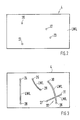
- FIG. 1 shows a schematic side view of two inserts 1 and 2, which are inserted into a frame (not shown).
- the two slots 1 and 2 are in the slot position.
- Inserts 1 and 2 have electronic circuits which e.g. belong to a broadband exchange.
- a signal connection device 3 is provided, by means of which communication paths between the inserts 1 and 2 are established.
- the broadband switching system can of course do more exist as only two inserts, but to illustrate the invention it is sufficient to only consider inserts 1 and 2.
- the signal connections of the communication paths between inserts 1 and 2 are designed as optical fibers.
- the rear wall 4 of the rack is included.
- the rear wall has a plate-shaped support 5, which forms a mechanical support.
- a support film 7 is applied over the entire surface and carries a flat optical waveguide LWL on its side 8 facing the inserts 1 and 2.
- optical waveguide LWL it is also possible for the optical waveguide LWL to be embedded in the carrier film 7.
- the insert 1 has a laser diode module.
- the light 10 generated by the laser diode module 9 is transmitted to an imaging optics 11, which is designed, for example, as a Selfoc lens.
- the bundled light 12 strikes the flat optical waveguide LWL at a coupling point 13 and is consequently transmitted up to a coupling point 14.
- the light 15 emanating from there is in turn bundled by means of imaging optics 16, the bundled light 17 being fed to a photodiode module 18. While the laser diode module 9 works as a transmitter, the photodiode module 18 represents a receiver.
- coupling structures 19 can be provided on the optical waveguide.
- an optical grating in particular a holographic grating, is formed there in each case.
- This grating can preferably be a sine grating, but according to a further exemplary embodiment also a triangular grating or else according to a further exemplary embodiment a sawtooth grating.
- the procedure is such that the periodicity of the grating (the distance between the individual columns of the grating) is matched to the wavelength of the light traveling in the optical waveguide.
- the respective grating it is also possible for the respective grating to have a different periodicity, that is to say, to have different distances between the individual columns, as viewed in terms of its spread.
- the aim is always for the light to be coupled into the optical waveguide with high efficiency and also to be coupled out with high efficiency. Since the shape and the direction of the light beam that is coupled in and out at the coupling point by means of the grating depends on the wavelength of the light, wavelength division multiplex connections are also possible. For example, two transmitters and two (or more) receivers on different wavelengths then work via an optical fiber (unidirectional operation). Furthermore, bidirectional operation is also possible, with two different wavelengths then Serve directional separation. There is then a transmitter and a receiver on each slot.
- FIG. 3 shows a further rear wall 4 which, compared to that of FIG. 2, does not have a full-surface optical waveguide, but a strip-shaped optical waveguide.
- coupling points 24, 25, 26 and 27 can be connected to coupling points 28, 29, 30 and 31, each of which, as already described in FIG. 1, lie opposite corresponding imaging optics of the associated plug-in units.
- the structure of the rear wall 4 in FIG. 3 corresponds to that in FIG Rear wall 4 housed so that there is no mutual interference.
- openings 33 can be formed in the carrier film, in which conductor tracks 34 are located. These are arranged on the side 6 of the carrier 5. They interact with spring contacts 35 of inserts 1 and 2 (not shown for insert 1). These measures make it possible to establish electrical connection paths between the inserts 1 and 2. Furthermore, these electrical contact connections can be used for supplying the supply voltage.
- wavelength multiplex connections are also possible.
- FIG. 4 For example, two laser diode modules 9a, 9b work as transmitters or receivers on different wavelengths via an optical waveguide (unidirectional operation). However, as already mentioned, bidirectional operation is also possible if the directions are separated by means of the different wavelengths. There is then a transmitter and a receiver on each slot.
- the imaging optics are identified by 11a and 11b.
- the light bears the reference numerals 10a, 10b or 12a and 12b.
- the lightwave multiplexer is an inherent part of the Fiber optic inputs and outputs are. This means that they are not part of interchangeable assemblies (inserts).
Landscapes
- Physics & Mathematics (AREA)
- General Physics & Mathematics (AREA)
- Optics & Photonics (AREA)
- Optical Couplings Of Light Guides (AREA)
- Optical Communication System (AREA)
- Optical Integrated Circuits (AREA)
- Mounting Of Printed Circuit Boards And The Like (AREA)
- Details Of Connecting Devices For Male And Female Coupling (AREA)
- Coupling Device And Connection With Printed Circuit (AREA)
- Mechanical Coupling Of Light Guides (AREA)
- Light Guides In General And Applications Therefor (AREA)
Applications Claiming Priority (2)
| Application Number | Priority Date | Filing Date | Title |
|---|---|---|---|
| DE4003056 | 1990-02-02 | ||
| DE4003056A DE4003056A1 (de) | 1990-02-02 | 1990-02-02 | Optische signalverbindungsvorrichtung fuer einschuebe eines einschubgestells |
Publications (3)
| Publication Number | Publication Date |
|---|---|
| EP0440087A2 true EP0440087A2 (fr) | 1991-08-07 |
| EP0440087A3 EP0440087A3 (en) | 1992-06-03 |
| EP0440087B1 EP0440087B1 (fr) | 1995-11-29 |
Family
ID=6399266
Family Applications (1)
| Application Number | Title | Priority Date | Filing Date |
|---|---|---|---|
| EP91100887A Expired - Lifetime EP0440087B1 (fr) | 1990-02-02 | 1991-01-24 | Dispositif de connexion de signaux optiques pour les tiroirs d'un boîtier à tiroir |
Country Status (7)
| Country | Link |
|---|---|
| US (1) | US5091985A (fr) |
| EP (1) | EP0440087B1 (fr) |
| JP (1) | JP2705853B2 (fr) |
| AT (1) | ATE130942T1 (fr) |
| CA (1) | CA2035530C (fr) |
| DE (2) | DE4003056A1 (fr) |
| ES (1) | ES2082868T3 (fr) |
Cited By (3)
| Publication number | Priority date | Publication date | Assignee | Title |
|---|---|---|---|---|
| EP0530551A1 (fr) * | 1991-09-04 | 1993-03-10 | Siemens Aktiengesellschaft | Appareil pour la réalisation d'une multiplicité de connexions à haute fréquence entre deux dispositifs de circuit pour le traitement parallèle de données |
| EP0604050A1 (fr) * | 1992-12-23 | 1994-06-29 | AT&T Corp. | Rachis optique de connexion |
| DE102006042254A1 (de) * | 2006-09-08 | 2008-03-27 | Siemens Ag | Reiheneinbaugerät und Reiheneinbaugeräte-Bussystem |
Families Citing this family (6)
| Publication number | Priority date | Publication date | Assignee | Title |
|---|---|---|---|---|
| GB2311381A (en) * | 1996-03-22 | 1997-09-24 | Northern Telecom Ltd | Equipment modules and backplane with optical connection |
| DE19823587A1 (de) | 1998-05-27 | 1999-12-02 | Alcatel Sa | Optische Verbindung sowie Verbindungseinheit zum Austausch von Daten zwischen Geräten |
| DE10053670A1 (de) * | 2000-10-28 | 2002-05-08 | Daimler Chrysler Ag | Optisches Signalübertragungssystem |
| FR2825858B1 (fr) * | 2001-06-11 | 2003-08-15 | Schneider Electric Ind Sa | Dispositif de communication optique entre des modules electroniques |
| DE10239575B3 (de) * | 2002-08-23 | 2004-02-12 | Erni Elektroapparate Gmbh | Steckverbinder zwischen einer Leiterplatte und einer Backplane |
| GB2426831B (en) * | 2005-06-01 | 2007-04-25 | Xyratex Tech Ltd | An optical connector, a communication system and a method of connecting a user circuit to an optical backplane |
Family Cites Families (8)
| Publication number | Priority date | Publication date | Assignee | Title |
|---|---|---|---|---|
| US3674914A (en) * | 1968-02-09 | 1972-07-04 | Photocircuits Corp | Wire scribed circuit boards and method of manufacture |
| US4465333A (en) * | 1982-01-15 | 1984-08-14 | Grumman Aerospace Corporation | Electro-optical plug-in interconnection |
| US4432604A (en) * | 1982-04-28 | 1984-02-21 | Bell Telephone Laboratories, Incorporated | Self-adjusting fiberoptic connector assembly |
| CA1249742A (fr) * | 1983-12-08 | 1989-02-07 | Yves Tremblay | Coupleur en etoile pour fibres optiques |
| FR2590995B1 (fr) * | 1985-02-26 | 1988-08-19 | Thomson Csf | Dispositif d'interconnexion optique de cartes de composants electroniques dans un coffret et procede de fabrication |
| US4732446A (en) * | 1985-10-02 | 1988-03-22 | Lamar Gipson | Electrical circuit and optical data buss |
| CA1260744A (fr) * | 1986-03-12 | 1989-09-26 | Northern Telecom Limited | Monture pour conducteurs optiques |
| GB8629921D0 (en) * | 1986-12-15 | 1987-01-28 | Gec Avionics | Optical backplanes |
-
1990
- 1990-02-02 DE DE4003056A patent/DE4003056A1/de not_active Withdrawn
-
1991
- 1991-01-16 US US07/640,799 patent/US5091985A/en not_active Expired - Fee Related
- 1991-01-24 AT AT91100887T patent/ATE130942T1/de not_active IP Right Cessation
- 1991-01-24 DE DE59106959T patent/DE59106959D1/de not_active Expired - Fee Related
- 1991-01-24 EP EP91100887A patent/EP0440087B1/fr not_active Expired - Lifetime
- 1991-01-24 ES ES91100887T patent/ES2082868T3/es not_active Expired - Lifetime
- 1991-01-31 JP JP3010605A patent/JP2705853B2/ja not_active Expired - Fee Related
- 1991-02-01 CA CA002035530A patent/CA2035530C/fr not_active Expired - Fee Related
Cited By (3)
| Publication number | Priority date | Publication date | Assignee | Title |
|---|---|---|---|---|
| EP0530551A1 (fr) * | 1991-09-04 | 1993-03-10 | Siemens Aktiengesellschaft | Appareil pour la réalisation d'une multiplicité de connexions à haute fréquence entre deux dispositifs de circuit pour le traitement parallèle de données |
| EP0604050A1 (fr) * | 1992-12-23 | 1994-06-29 | AT&T Corp. | Rachis optique de connexion |
| DE102006042254A1 (de) * | 2006-09-08 | 2008-03-27 | Siemens Ag | Reiheneinbaugerät und Reiheneinbaugeräte-Bussystem |
Also Published As
| Publication number | Publication date |
|---|---|
| US5091985A (en) | 1992-02-25 |
| EP0440087B1 (fr) | 1995-11-29 |
| EP0440087A3 (en) | 1992-06-03 |
| ATE130942T1 (de) | 1995-12-15 |
| JPH04213896A (ja) | 1992-08-04 |
| DE59106959D1 (de) | 1996-01-11 |
| CA2035530C (fr) | 1996-12-31 |
| DE4003056A1 (de) | 1991-08-08 |
| JP2705853B2 (ja) | 1998-01-28 |
| ES2082868T3 (es) | 1996-04-01 |
| CA2035530A1 (fr) | 1991-08-03 |
Similar Documents
| Publication | Publication Date | Title |
|---|---|---|
| DE69020732T2 (de) | Rückwand für optische fasern. | |
| DE3874839T2 (de) | Opto-elektrische verbindungsmittel. | |
| DE69535189T2 (de) | Optische rückwandverdrahtungsverbindung | |
| EP1390790B1 (fr) | Dispositif de repartition optique et cable de connexion de guides d'ondes optiques | |
| EP0824714B1 (fr) | Systeme de prises electriques | |
| DE69836058T2 (de) | Mehrkanaliges optisches Empfänger-/Sendersystem | |
| DE69214593T2 (de) | Optisches Verbindungssystem für Elektronikplatinen | |
| EP0040706B1 (fr) | Système de communication optique | |
| EP0061772B1 (fr) | Module prise électro-optique | |
| WO2004092797A1 (fr) | Module coupleur a fibres de verre | |
| EP0783717A1 (fr) | Dispositif de raccordement d'appareils electroniques a mettre en communication les uns avec les autres | |
| DE69022259T2 (de) | Optische Verbindungsnetz. | |
| DE19711121B4 (de) | Verzweigende Lichtwellenleiteranordnung und verzweigendes Lichtwellenleiterarray | |
| EP0440087A2 (fr) | Dispositif de connexion de signaux optiques pour les tiroirs d'un boîtier à tiroir | |
| EP2502105A2 (fr) | Procédé de fabrication d'un ensemble optique, ensemble optique et cascade de séparateurs | |
| EP0909121B1 (fr) | Module électronique d'entrée / sortie | |
| DE3739629C2 (fr) | ||
| DE10229428A1 (de) | Detektoreinheit | |
| DE2715846C3 (de) | Lichtkoppelndes Bauelement für gedruckte Schaltungen | |
| DE3624653C2 (de) | Optischer Biegekoppler mit Prüfstift, insbesondere für eine Vielzahl von Lichtwellenleitern | |
| EP1180704A2 (fr) | Connecteur et système pour la connection électrique de supports comprenant des composants électriques dans le domaine des télécommunications | |
| DE60104683T2 (de) | Optische anordnung | |
| DE10036237A1 (de) | Ein-und/oder Ausgabebaugruppe zur Verwendung in einem Steuerungssystem | |
| DE4101962A1 (de) | Anordnung zur uebertragung von daten mit mindestens einem lichtwellenleiter | |
| DE102004027068B3 (de) | Schaltung zur Signalübertragung in einem Netzwerkknoten, insbesondere für eine Kanalkarte für eine optische WDM-Signalübertragungseinrichtung |
Legal Events
| Date | Code | Title | Description |
|---|---|---|---|
| PUAI | Public reference made under article 153(3) epc to a published international application that has entered the european phase |
Free format text: ORIGINAL CODE: 0009012 |
|
| AK | Designated contracting states |
Kind code of ref document: A2 Designated state(s): AT BE CH DE ES FR GB IT LI NL SE |
|
| PUAL | Search report despatched |
Free format text: ORIGINAL CODE: 0009013 |
|
| AK | Designated contracting states |
Kind code of ref document: A3 Designated state(s): AT BE CH DE ES FR GB IT LI NL SE |
|
| RAP3 | Party data changed (applicant data changed or rights of an application transferred) |
Owner name: ALCATEL N.V. Owner name: ALCATEL SEL AKTIENGESELLSCHAFT |
|
| 17P | Request for examination filed |
Effective date: 19921030 |
|
| 17Q | First examination report despatched |
Effective date: 19940525 |
|
| GRAA | (expected) grant |
Free format text: ORIGINAL CODE: 0009210 |
|
| AK | Designated contracting states |
Kind code of ref document: B1 Designated state(s): AT BE CH DE ES FR GB IT LI NL SE |
|
| REF | Corresponds to: |
Ref document number: 130942 Country of ref document: AT Date of ref document: 19951215 Kind code of ref document: T |
|
| REF | Corresponds to: |
Ref document number: 59106959 Country of ref document: DE Date of ref document: 19960111 |
|
| ITF | It: translation for a ep patent filed | ||
| REG | Reference to a national code |
Ref country code: CH Ref legal event code: NV Representative=s name: JUERG ULRICH C/O ALCATEL STR AG |
|
| ET | Fr: translation filed | ||
| GBT | Gb: translation of ep patent filed (gb section 77(6)(a)/1977) |
Effective date: 19960215 |
|
| REG | Reference to a national code |
Ref country code: ES Ref legal event code: FG2A Ref document number: 2082868 Country of ref document: ES Kind code of ref document: T3 |
|
| PLBE | No opposition filed within time limit |
Free format text: ORIGINAL CODE: 0009261 |
|
| STAA | Information on the status of an ep patent application or granted ep patent |
Free format text: STATUS: NO OPPOSITION FILED WITHIN TIME LIMIT |
|
| 26N | No opposition filed | ||
| PGFP | Annual fee paid to national office [announced via postgrant information from national office to epo] |
Ref country code: NL Payment date: 19991216 Year of fee payment: 10 |
|
| PGFP | Annual fee paid to national office [announced via postgrant information from national office to epo] |
Ref country code: CH Payment date: 19991217 Year of fee payment: 10 |
|
| PGFP | Annual fee paid to national office [announced via postgrant information from national office to epo] |
Ref country code: AT Payment date: 19991221 Year of fee payment: 10 |
|
| PGFP | Annual fee paid to national office [announced via postgrant information from national office to epo] |
Ref country code: BE Payment date: 20000107 Year of fee payment: 10 |
|
| PG25 | Lapsed in a contracting state [announced via postgrant information from national office to epo] |
Ref country code: AT Free format text: LAPSE BECAUSE OF NON-PAYMENT OF DUE FEES Effective date: 20010124 |
|
| PG25 | Lapsed in a contracting state [announced via postgrant information from national office to epo] |
Ref country code: LI Free format text: LAPSE BECAUSE OF NON-PAYMENT OF DUE FEES Effective date: 20010131 Ref country code: CH Free format text: LAPSE BECAUSE OF NON-PAYMENT OF DUE FEES Effective date: 20010131 Ref country code: BE Free format text: LAPSE BECAUSE OF NON-PAYMENT OF DUE FEES Effective date: 20010131 |
|
| BERE | Be: lapsed |
Owner name: ALCATEL N.V. Effective date: 20010131 |
|
| PG25 | Lapsed in a contracting state [announced via postgrant information from national office to epo] |
Ref country code: NL Free format text: LAPSE BECAUSE OF NON-PAYMENT OF DUE FEES Effective date: 20010801 |
|
| REG | Reference to a national code |
Ref country code: CH Ref legal event code: PL |
|
| NLV4 | Nl: lapsed or anulled due to non-payment of the annual fee |
Effective date: 20010801 |
|
| PGFP | Annual fee paid to national office [announced via postgrant information from national office to epo] |
Ref country code: GB Payment date: 20011214 Year of fee payment: 12 |
|
| PGFP | Annual fee paid to national office [announced via postgrant information from national office to epo] |
Ref country code: DE Payment date: 20011217 Year of fee payment: 12 |
|
| PGFP | Annual fee paid to national office [announced via postgrant information from national office to epo] |
Ref country code: FR Payment date: 20011226 Year of fee payment: 12 |
|
| REG | Reference to a national code |
Ref country code: GB Ref legal event code: IF02 |
|
| PGFP | Annual fee paid to national office [announced via postgrant information from national office to epo] |
Ref country code: SE Payment date: 20020102 Year of fee payment: 12 |
|
| PGFP | Annual fee paid to national office [announced via postgrant information from national office to epo] |
Ref country code: ES Payment date: 20020118 Year of fee payment: 12 |
|
| PG25 | Lapsed in a contracting state [announced via postgrant information from national office to epo] |
Ref country code: GB Free format text: LAPSE BECAUSE OF NON-PAYMENT OF DUE FEES Effective date: 20030124 |
|
| PG25 | Lapsed in a contracting state [announced via postgrant information from national office to epo] |
Ref country code: SE Free format text: LAPSE BECAUSE OF NON-PAYMENT OF DUE FEES Effective date: 20030125 Ref country code: ES Free format text: LAPSE BECAUSE OF NON-PAYMENT OF DUE FEES Effective date: 20030125 |
|
| PG25 | Lapsed in a contracting state [announced via postgrant information from national office to epo] |
Ref country code: DE Free format text: LAPSE BECAUSE OF NON-PAYMENT OF DUE FEES Effective date: 20030801 |
|
| EUG | Se: european patent has lapsed | ||
| GBPC | Gb: european patent ceased through non-payment of renewal fee | ||
| PG25 | Lapsed in a contracting state [announced via postgrant information from national office to epo] |
Ref country code: FR Free format text: LAPSE BECAUSE OF NON-PAYMENT OF DUE FEES Effective date: 20030930 |
|
| REG | Reference to a national code |
Ref country code: FR Ref legal event code: ST |
|
| REG | Reference to a national code |
Ref country code: ES Ref legal event code: FD2A Effective date: 20030125 |
|
| PG25 | Lapsed in a contracting state [announced via postgrant information from national office to epo] |
Ref country code: IT Free format text: LAPSE BECAUSE OF NON-PAYMENT OF DUE FEES;WARNING: LAPSES OF ITALIAN PATENTS WITH EFFECTIVE DATE BEFORE 2007 MAY HAVE OCCURRED AT ANY TIME BEFORE 2007. THE CORRECT EFFECTIVE DATE MAY BE DIFFERENT FROM THE ONE RECORDED. Effective date: 20050124 |