EP0440243A2 - Dispositif de commande de mémoire pour subunité-mémoire tel que mémoires à disques - Google Patents
Dispositif de commande de mémoire pour subunité-mémoire tel que mémoires à disques Download PDFInfo
- Publication number
- EP0440243A2 EP0440243A2 EP91101312A EP91101312A EP0440243A2 EP 0440243 A2 EP0440243 A2 EP 0440243A2 EP 91101312 A EP91101312 A EP 91101312A EP 91101312 A EP91101312 A EP 91101312A EP 0440243 A2 EP0440243 A2 EP 0440243A2
- Authority
- EP
- European Patent Office
- Prior art keywords
- memory
- data
- signal
- unit
- interface unit
- Prior art date
- Legal status (The legal status is an assumption and is not a legal conclusion. Google has not performed a legal analysis and makes no representation as to the accuracy of the status listed.)
- Withdrawn
Links
Images


Classifications
-
- G—PHYSICS
- G06—COMPUTING OR CALCULATING; COUNTING
- G06F—ELECTRIC DIGITAL DATA PROCESSING
- G06F12/00—Accessing, addressing or allocating within memory systems or architectures
- G06F12/02—Addressing or allocation; Relocation
- G06F12/08—Addressing or allocation; Relocation in hierarchically structured memory systems, e.g. virtual memory systems
- G06F12/0802—Addressing of a memory level in which the access to the desired data or data block requires associative addressing means, e.g. caches
- G06F12/0866—Addressing of a memory level in which the access to the desired data or data block requires associative addressing means, e.g. caches for peripheral storage systems, e.g. disk cache
Definitions
- the present invention relates to a controller for controlling an external storage or sub-memory unit such as a hard disk drive, a floppy disk drive, an optical disk drive and a cartridge magnetic tape drive employed in an information processing system and, more particularly, to an improvement in a data transfer control unit in such a memory controller.
- an external storage or sub-memory unit such as a hard disk drive, a floppy disk drive, an optical disk drive and a cartridge magnetic tape drive employed in an information processing system and, more particularly, to an improvement in a data transfer control unit in such a memory controller.
- An information processing system which processes, manages and stores a great amount of data, includes one or more external storage or sub-memory units described above in addition to a main memory unit.
- a memory controller is thus required which intervenes between a host processor and the sub-memory unit to perform a data transfer operation therebetween.
- such a memory controller includes an interface control unit for interfacing with the host processor, a buffer memory for temporarily storing data read from or to be written into the sub-memory unit, and a data transfer control unit for performing a data transfer operation between the interface control unit and the buffer memory.
- the memory controller writes data from the host processor into the sub-memory unit and reads data from the sub-memory unit to the host processor.
- the host processor often requires to obtain data that are the same as the data which were written into or read from the sub-memory unit by the previous request. Even in such a case, if the memory controller is constructed to perform the data read operation from the sub-memory unit whenever the access request is generated from the host processor, it takes a relatively long time to transfer the required data to the host processor. This is because the access speed of the sub-memory unit is slow.
- the memory controller is constructed to be connected with or to include a cash memory for storing a part of data written in the sub-memory unit and the data transfer control unit is added with a function of controlling the cash memory. Accordingly, if the cash memory stores data that are the same as the data required by the host processor, those data are read out of the cash memory and then transferred via the interface unit to the host processor. No data read operation from the sub-memory unit is thus required. On the other hand, in case where the cash memory does not store the data required by the host processor, the data read operation from the sub-memory unit is initiated.
- the data read from the sub-memory unit is first temporarily stored in the buffer memory.
- the data thus stored in the buffer memory is then transferred to the cash memory under the control of the data transfer control unit. Thereafter, the data read operation from the cash memory is initiated, so that the data is transferred to the interface unit from the cash memory and finally to the host processor.
- the data transfer speed is improved remarkably in case of the cash memory storing the required data, but the data transfer speed is lowered extremely in case of the cash memory not storing the required data since the data read out of the sub-memory unit is transferred from the buffer memory to the interface unit under the intervention of the cash memory.
- the host processor requires to write data into the sub-memory unit, those data are first stored into the cash memory from the interface unit and thereafter transferred to the buffer memory from the cash memory. The data write speed into the sub-memory unit is thereby lowered.
- an object of the present invention is to provide an improved controller for performing a data transfer between a host processor and an external storage or sub-memory unit at a high speed.
- Another object of the present invention is to provide a memory controller capable of performing a data transfer from an interface unit coupled to a host processor simultaneously to both of a buffer memory coupled to an external storage (sub-memory) unit and a cash memory and/or from the buffer memory simultaneously to both of the interface unit and the cash memory.
- a controller coupled to a host processor, an external storage unit and a cash memory for performing a data transfer thereamong, comprising an interface unit coupled to the host processor, a buffer memory coupled to the external storage unit, a data transfer control unit, and a bus for interconnecting the interface unit, the buffer memory and the cash memory to one another.
- the interface unit includes a selection terminal supplied with a first selection signal, a read terminal supplied with a first read signal and a write terminal supplied with a first write signal, outputs data therein onto the bus in response to the first read signal while receiving the first selection signal and fetches data on the bus in response to the first write signal while receiving the first selection signal.
- the buffer memory includes a selection terminal supplied with a second selection signal, a read terminal supplied with a second read signal and a write terminal supplied with a second write signal, outputs data therein onto the bus in response to the second read signal while receiving the second selection signal and fetches data on bus in response to the second write signal while receiving the second selection signal.
- the cash memory receives memory read and write signals.
- the memory read signal causes the cash memory to output data therein onto the bus and the memory write signal cause the cash memory to fetch data on the bus.
- the data transfer control unit controls the above-mentioned signals such that the first and second selection signals are generated at the substantially same time and the first (or second) read signal, the second (or first) write signal and the memory write signal are then generated.
- the data from the interface unit is transferred simultaneously to both of the buffer memory and the cash memory or the data from the buffer memory is transferred simultaneously to both of the interface unit and the cash memory.
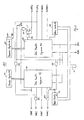
- a memory controller 1 is fabricated as an integrated circuit device and includes an interface control unit 30, a data transfer control unit 40, a buffer memory 50 and a format control unit 60.
- the interface control unit 30 interfaces with a host processor 2 in a so-called SCSI (Small Computer System Interface) method and is thus coupled through a first set of terminals 10 and a SCSI bus 21 to the host processor 2.
- the format control unit 60 is coupled through a second set of terminals 12 and a communication bus 41 to a sub-memory unit 4 to read or write data from or into the unit 4.
- a hard disk drive is used as the unit 4.
- the data to be written into the sub-memory unit 4 and the data read therefrom are transferred between the format control unit and the buffer memory 50.
- a FIFO (First-in First-Out) type memory can be used as the buffer memory 50.
- the interface control unit 30, the data memory 50 and the format control unit 60 are interconnected via a internal processor bus 17 to a third set of terminals 11 which is in turn coupled to a microprocessor 3 via an external processor bus 31.
- the microprocessor 3 controls operations of the memory controller 1.
- the data transfer control unit 40 is further coupled to the bus 17. In this embodiment, this control unit 40 performs a data transfer operation in a DMA (Direct Memory Access) transfer manner. More specifically, the control unit 40 receives from the interface unit 30 a first data transfer request signal DRQ1 representing that the unit 30 is in a ready condition for outputting data transferred from the host processor 2 or receiving data to be transferred thereto and from the buffer memory a second data transfer request signal DRQ2 representing that the memory 30 is in a ready condition for outputting data transferred from the format control unit 60 or receiving data to be transferred thereto. In response to the request signal DRQ1, the unit 40 returns an acknowledge signal DAK1 to the interface unit 30 to bring the unit 30 into an activated condition.
- DMA Direct Memory Access
- the unit 40 also responds to the request signal DRQ2 and returns an acknowledge signal DAK2 to the buffer memory 50 to bring the memory 50 into an activated condition.
- the acknowledge signals DAK1 and DAK2 thus serve as a chip-select signal for the corresponding unit.
- the data transfer control unit 40 generates data read and write control signals that causes the unit 30 or the memory 50 to output data stored therein and to fetch data supplied thereto, respectively, it generates the data read and write control signals IORD1 and IOWR1 for the interface unit 30 and those IORD2 and IOWR2 for the buffer memory 50 independently of each other in accordance with the present invention.
- the read control signals IORD1 and IORD2 indicate a data read timing at which the unit 30 and the memory 50 are to output the data stored therein, respectively, and the write control signals IOWR1 and IOWR2 indicate a data write timing at which the unit 30 and the memory 50 is to fetch the data supplied thereto.
- the data transfer between the unit 30 and the memory 50 is carried out via an internal data bus 19 to which the transfer control unit 40 and a fourth set of terminals 13 are further coupled.
- the set of terminals 13 is coupled to a cash memory 5 which is provided externally.
- the data transfer control unit 40 further generates address information and memory read and write control signals MRD and MWR.
- the address information is transferred via an address bus 21 and a fifth set of terminals 14 to the cash memory 5 and the signals MRD and MWR are supplied via terminals 15 and 16 thereto.
- the data transfer control unit 40 includes a pair of parameter registers 401 and 501, a pair of data transfer sequencers 403 and 503 and a pair of address counters 404 and 504.
- the register 401, the sequencer 403 and the counter 404 are allotted to the data memory 50 and the register 501, the sequencer 503 and the counter 504 are allotted to the interface control unit 30.
- Each of the registers 401 and 501 is set by the microprocessor 3 with parameter data including transfer direction information for designating a data transfer direction, byte-number information for representing the number of byte data to be transferred, transfer-enable information for allowing a data transfer and so forth.
- Each of the address counters 404 add 504 are also set by the microprocessor 3 with a start address for designating a data transfer start address of the cash memory 5.
- the sequencers 403 and 503 produce the control signals DAK1 and 2, IORD1 and 2, IOWR1 and 2, MRD and MWR in a predetermined sequence and update the addresses of the counters 404 and 405, respectively.
- the parameter register 401 has an additional mode flag 402 which is set to "1" when the simultaneous data transfer from the data memory 50 to the cash memory 5 and to the interface unit 30 is performed and reset to "0" when other data transfers are performed.
- the microprocessor 3 sets or resets the flag 402.
- the interface control unit 30 receives from the host processor 2 a command that the host processor 2 requires data from the sub-memory unit 4, the unit 30 transfers that command to the microprocessor 3 via the buses 17 and 31 and the terminals 31.
- the microprocessor 3 is provided with a memory for storing sector and tag information representative of a data area of the sub-memory unit 4 stored by the cash memory 5. The microprocessor 3 decodes the command supplied thereto and judges whether or not the data required by the host processor 2 are stored in the cash memory 5 in response to the sector and tag information.
- the microprocessor 3 supplies the parameter register 501 and the address counter 504 with a set of information necessary for the data transfer between the interface unit 30 and the cash memory 5.
- the parameter register 401 is set with data including transfer-disable information deactivating the sequencer 403.
- the flag 402 is also reset to "0".
- the data transfer between the unit 30 and the memory 5 is brought into an enable-condition. In this condition, when the sequencer 503 receives the request signal DRQ1 from the unit 30, it returns the acknowledge signal DAK1 to the unit 30 via the OR gate 456.
- the sequencer instructs the address counter 504 to supply the address information to the cash memory 5 through the bus 21 and the terminal 14, and further generates the memory read signal MRD and the data write control signal IOWR1.
- the data stored in an address location of the cash memory 5 designated by the address information supplied thereto is read out therefrom and then transferred to the interface control unit 30 via the bus 19. This data is in turn transferred to the host processor 2 from the unit 30.
- the address of the counter 504 is thereafter updated. The operation described above is repeated until the data thus transferred reaches the number of byte data to be transferred.
- the present data transfer control unit 40 transfers simultaneously the data from the buffer memory 50 to both of the cash memory 5 and the interface unit 30 in the following manner.
- the microprocessor 3 supplies the format control unit 60 with control information necessary to read data from the unit 4.
- the microprocessor 3 also supplies the parameter register 401 and the counter 404 with information necessary for the data transfer between the buffer memory 50 and the cash memory 5 and further sets the flag 402 to "1".
- the parameter register 501 is supplied with the transfer-disable information for deactiving the sequencer 503.
- both of the buffer memory 50 and the interface unit 30 are required to be in a ready condition.
- the AND gates 451 and 453 detect the generation of both request signals DRQ1 and DRQ2.
- the data transfer sequencer 402 receives a true data request signal.
- the sequencer 402 returns the acknowledge signal DAK2 to the buffer memory 50. Since the sequencer 503 is deactivated, it does not produce the acknowledge signal even when receiving the request signal DRQ1.
- the generation of the acknowledge signal DAK2 causes the generation of the acknowledge signal DAK1 through the AND gate 454 and the OR gate 456, as shown in Fig. 3.
- the sequencer 402 then generates the read signal IORD2 and further instructs the address counter 404 to output the address information thereof which is in turn transferred via the bus 21 to the cash memory 5.
- the buffer memory 50 reads the data therein onto the bus 19.
- the sequencer 402 further generates the memory write signal MWR which is in turn supplied to the memory 5 via the terminal 15.
- the sequencer 503 does not generate the write control signal
- the generation of the memory write signal MWR causes the generation of the write control signal IOWR1 through the AND gate 458 and the OR gate 457.
- the data onto the bus 19, which is read out of the buffer memory 50 is transferred to both of the cash memory 5 and the interface unit 30 simultaneously.
- the address of the counter 404 is thereafter updated.
- the buffer memory 50 and the interface unit 30 changes the request signals DRQ2 and DRQ1 to the low level, respectively.
- the data from the buffer memory 50 is transferred simultaneously to both of the cash memory 5 and the interface unit 30, so that the speed of the data transfer is not lowered.
- the data from the buffer memory 50 is transferred only to the cash memory 5.
- the data thus stored in the memory 5 is then transferred to the unit 30 by use of the sequencer 503 and the counter 504.
- the above embodiment does not have a construction for transferring the data, which is supplied from the host processor 2, from the interface unit 30 simultaneously to both of the cash memory 5 and the data buffer 50. For this reason, the data is first transferred from the interface unit 30 to the cash memory 5 by use of the sequencer 503 and then transferred from the cash memory 5 to the buffer memory 50 by use of the sequencer 403.
- FIG. 4 A construction for transferring data from the interface unit 30 simultaneously to both of the buffer and cash memories 50 and 5 is shown in Fig. 4 as another embodiment of the present invention.
- the same constituents as those shown in Fig. 2 are denoted by the same reference numerals to omit further description thereof.
- the parameter register 501 includes a flag 502 set to "1" or reset to "0" by the microprocessor 3.
- the microprocessor 3 when the microprocessor 3 detects that the host processor 2 requires to write data into the sub-memory unit 4 in response to the information from the interface unit 30, it supplies the register 501 and the counter 504 with information necessary to the data transfer between the unit 30 and the cash memory 5 and further sets the flag 502 to "1". Accordingly, when both of the interface unit 30 and the buffer memory 50 are in a ready condition, as shown in Fig. 5, the sequencer 503 receives a true data request signal. In response thereto, the sequencer 503 returns the acknowledge signal DAK1 to the unit 30 and further instructs the counter 504 to output the address. The generation of the signal DAK1 results in generation of the acknowledge signal DAK2 through the gates 601 and 606, as shown in Fig. 5.
- the sequencer 503 then generates the read signal IORD1 to the unit 30 and the write signal MWR to the cash memory 5.
- the generation of the signal MWR causes the generation of the write signal IOWR2 to the buffer memory 50 through the gates 608 and 607, as shown in Fig. 3.
- the data read out from the interface unit 30 is transferred simultaneously to both of the cash memory 5 and the buffer memory 50.
- microprocessor 3 and/or the cash memory 5 may be incorporated into the memory controller 1 as a single integrated circuit chip.
Landscapes
- Engineering & Computer Science (AREA)
- Theoretical Computer Science (AREA)
- Physics & Mathematics (AREA)
- General Engineering & Computer Science (AREA)
- General Physics & Mathematics (AREA)
- Memory System Of A Hierarchy Structure (AREA)
Applications Claiming Priority (4)
| Application Number | Priority Date | Filing Date | Title |
|---|---|---|---|
| JP22644/90 | 1990-01-31 | ||
| JP2022644A JPH03226850A (ja) | 1990-01-31 | 1990-01-31 | 外部補助記憶制御装置 |
| JP4014590 | 1990-02-20 | ||
| JP40145/90 | 1990-02-20 |
Publications (2)
| Publication Number | Publication Date |
|---|---|
| EP0440243A2 true EP0440243A2 (fr) | 1991-08-07 |
| EP0440243A3 EP0440243A3 (en) | 1993-12-15 |
Family
ID=26359904
Family Applications (1)
| Application Number | Title | Priority Date | Filing Date |
|---|---|---|---|
| EP19910101312 Withdrawn EP0440243A3 (en) | 1990-01-31 | 1991-01-31 | Memory controller for sub-memory unit such as disk drives |
Country Status (2)
| Country | Link |
|---|---|
| US (1) | US5307471A (fr) |
| EP (1) | EP0440243A3 (fr) |
Cited By (2)
| Publication number | Priority date | Publication date | Assignee | Title |
|---|---|---|---|---|
| EP0593174A3 (en) * | 1992-10-08 | 1996-09-04 | Ibm | Dual actuator dasd |
| CN102375698A (zh) * | 2010-08-23 | 2012-03-14 | 群联电子股份有限公司 | 数据串分派与传送方法、存储器控制器与存储器储存装置 |
Families Citing this family (17)
| Publication number | Priority date | Publication date | Assignee | Title |
|---|---|---|---|---|
| US5644787A (en) * | 1993-08-03 | 1997-07-01 | Seiko Epson Corporation | Apparatus for controlling data transfer between external interfaces through buffer memory using table data having transfer start address transfer count and unit selection parameter |
| WO1995006280A2 (fr) * | 1993-08-26 | 1995-03-02 | Electronic Arts, Inc. | Appareil et procede permettant d'accelerer le transfert de donnees |
| JPH07210500A (ja) * | 1994-01-25 | 1995-08-11 | Fujitsu Ltd | データ転送制御装置 |
| JPH07253929A (ja) * | 1994-03-14 | 1995-10-03 | Hitachi Ltd | 半導体記憶装置 |
| JP2790034B2 (ja) * | 1994-03-28 | 1998-08-27 | 日本電気株式会社 | 非運用系メモリ更新方式 |
| US5661848A (en) * | 1994-09-08 | 1997-08-26 | Western Digital Corp | Multi-drive controller with encoder circuitry that generates ECC check bytes using the finite field for optical data for appending to data flowing to HDA |
| US5606529A (en) * | 1994-12-20 | 1997-02-25 | Hitachi, Ltd. | Semiconductor disk storage |
| US5600602A (en) * | 1995-04-05 | 1997-02-04 | Micron Technology, Inc. | Hierarchical memory array structure having electrically isolated bit lines for temporary data storage |
| US5734620A (en) * | 1995-04-05 | 1998-03-31 | Micron Technology, Inc. | Hierarchical memory array structure with redundant components having electrically isolated bit lines |
| US5838934A (en) * | 1995-06-07 | 1998-11-17 | Texas Instruments Incorporated | Host port interface |
| JPH09251437A (ja) * | 1996-03-18 | 1997-09-22 | Toshiba Corp | 計算機装置及び連続データサーバ装置 |
| US5661680A (en) * | 1996-09-09 | 1997-08-26 | International Business Machines Corporation | Analog output buffer circuit |
| DE19638772A1 (de) * | 1996-09-21 | 1998-03-26 | Philips Patentverwaltung | Telekommunikationsgerät, insbesondere Mobilfunkendgerät |
| US6157984A (en) * | 1997-05-15 | 2000-12-05 | Seagate Technology, Llc | Integrated controller/processor for disc drive having direct memory access |
| US6151236A (en) * | 2000-02-29 | 2000-11-21 | Enhanced Memory Systems, Inc. | Enhanced bus turnaround integrated circuit dynamic random access memory device |
| JP4082913B2 (ja) * | 2002-02-07 | 2008-04-30 | 株式会社ルネサステクノロジ | メモリシステム |
| US8510493B2 (en) * | 2010-12-27 | 2013-08-13 | Lsi Corporation | Circuit to efficiently handle data movement within a cache controller or on-chip memory peripheral |
Family Cites Families (6)
| Publication number | Priority date | Publication date | Assignee | Title |
|---|---|---|---|---|
| US4157587A (en) * | 1977-12-22 | 1979-06-05 | Honeywell Information Systems Inc. | High speed buffer memory system with word prefetch |
| US4792898A (en) * | 1986-09-26 | 1988-12-20 | Mccarthy Donald F | Method and apparatus for temporarily storing multiple data records |
| US4851991A (en) * | 1987-02-24 | 1989-07-25 | Digital Equipment Corporation | Central processor unit for digital data processing system including write buffer management mechanism |
| US4831520A (en) * | 1987-02-24 | 1989-05-16 | Digital Equipment Corporation | Bus interface circuit for digital data processor |
| US5025366A (en) * | 1988-01-20 | 1991-06-18 | Advanced Micro Devices, Inc. | Organization of an integrated cache unit for flexible usage in cache system design |
| US5119485A (en) * | 1989-05-15 | 1992-06-02 | Motorola, Inc. | Method for data bus snooping in a data processing system by selective concurrent read and invalidate cache operation |
-
1991
- 1991-01-31 EP EP19910101312 patent/EP0440243A3/en not_active Withdrawn
- 1991-01-31 US US07/648,168 patent/US5307471A/en not_active Expired - Fee Related
Cited By (3)
| Publication number | Priority date | Publication date | Assignee | Title |
|---|---|---|---|---|
| EP0593174A3 (en) * | 1992-10-08 | 1996-09-04 | Ibm | Dual actuator dasd |
| CN102375698A (zh) * | 2010-08-23 | 2012-03-14 | 群联电子股份有限公司 | 数据串分派与传送方法、存储器控制器与存储器储存装置 |
| CN102375698B (zh) * | 2010-08-23 | 2014-06-25 | 群联电子股份有限公司 | 数据串分派与传送方法、存储器控制器与存储器储存装置 |
Also Published As
| Publication number | Publication date |
|---|---|
| EP0440243A3 (en) | 1993-12-15 |
| US5307471A (en) | 1994-04-26 |
Similar Documents
| Publication | Publication Date | Title |
|---|---|---|
| US5307471A (en) | Memory controller for sub-memory unit such as disk drives | |
| EP0489504B1 (fr) | Tampon FIFO bidirectionnel pour réaliser l'interfaçage entre deux barres omnibus | |
| JP3289661B2 (ja) | キャッシュメモリシステム | |
| EP0569969A1 (fr) | Microordinateur avec mémoire d'instruction stockant des instructions pour sortir des conditions internes | |
| US5404480A (en) | Information processor comprising a write buffer circuit containing an address buffer and a data buffer corresponding to each other | |
| US4607328A (en) | Data transfer apparatus for a microcomputer system | |
| EP0464848B1 (fr) | Structure permettant le transfert direct de mémoire à mémoire | |
| US5504673A (en) | Microprogram load unit | |
| EP0332151A2 (fr) | Dispositif de commande d'accès direct de mémoire | |
| EP0139254A2 (fr) | Appareil et méthode pour un transfert direct de données de mémoire vers un dispositif périphérique et du dispositif périphérique vers la mémoire | |
| JPS6365953B2 (fr) | ||
| CA2370596A1 (fr) | Systemes et procedes destines a une architecture de la memoire d'un controleur de disque dur | |
| JPH04332063A (ja) | ローカルコンピューティングシステムによるホストコンピューティングシステムへのアクセス制御を調整するためのローカルコンピューティングシステムとともに使用される装置 | |
| US5522061A (en) | Read concurrency through transaction synthesis | |
| JP3162459B2 (ja) | データ処理装置 | |
| JP2768022B2 (ja) | メモリコントローラ | |
| JPH02171843A (ja) | インターフェース装置 | |
| JP2892429B2 (ja) | 入出力制御装置 | |
| JPS62184560A (ja) | 入出力バツフア制御装置 | |
| JPH06250965A (ja) | 入出力制御装置 | |
| JP3331943B2 (ja) | 情報処理装置および入出力制御装置 | |
| JP3299147B2 (ja) | キャッシュ制御回路 | |
| EP0373393A1 (fr) | Système de traitement d'information | |
| JPS58213371A (ja) | デ−タ処理システム | |
| EP0369964A2 (fr) | Interface pour formats de données multiples |
Legal Events
| Date | Code | Title | Description |
|---|---|---|---|
| PUAI | Public reference made under article 153(3) epc to a published international application that has entered the european phase |
Free format text: ORIGINAL CODE: 0009012 |
|
| 17P | Request for examination filed |
Effective date: 19910131 |
|
| AK | Designated contracting states |
Kind code of ref document: A2 Designated state(s): DE FR GB |
|
| PUAL | Search report despatched |
Free format text: ORIGINAL CODE: 0009013 |
|
| AK | Designated contracting states |
Kind code of ref document: A3 Designated state(s): DE FR GB |
|
| 17Q | First examination report despatched |
Effective date: 19951121 |
|
| STAA | Information on the status of an ep patent application or granted ep patent |
Free format text: STATUS: THE APPLICATION HAS BEEN WITHDRAWN |
|
| 18W | Application withdrawn |
Withdrawal date: 19960124 |