EP0441201B1 - Circuit détecteur de la tension de polarisation du substrat - Google Patents
Circuit détecteur de la tension de polarisation du substrat Download PDFInfo
- Publication number
- EP0441201B1 EP0441201B1 EP91100961A EP91100961A EP0441201B1 EP 0441201 B1 EP0441201 B1 EP 0441201B1 EP 91100961 A EP91100961 A EP 91100961A EP 91100961 A EP91100961 A EP 91100961A EP 0441201 B1 EP0441201 B1 EP 0441201B1
- Authority
- EP
- European Patent Office
- Prior art keywords
- transistor
- detection circuit
- substrate bias
- voltage
- potential
- Prior art date
- Legal status (The legal status is an assumption and is not a legal conclusion. Google has not performed a legal analysis and makes no representation as to the accuracy of the status listed.)
- Expired - Lifetime
Links
- 239000000758 substrate Substances 0.000 title claims description 31
- 238000001514 detection method Methods 0.000 title claims description 24
- 238000005513 bias potential Methods 0.000 claims 3
- 230000003071 parasitic effect Effects 0.000 description 8
- 238000005516 engineering process Methods 0.000 description 3
- 230000000295 complement effect Effects 0.000 description 2
- 238000000034 method Methods 0.000 description 2
- 239000004065 semiconductor Substances 0.000 description 2
- 238000010276 construction Methods 0.000 description 1
- 230000001066 destructive effect Effects 0.000 description 1
- 238000010586 diagram Methods 0.000 description 1
- 238000010304 firing Methods 0.000 description 1
- 230000001052 transient effect Effects 0.000 description 1
Images

Classifications
-
- G—PHYSICS
- G11—INFORMATION STORAGE
- G11C—STATIC STORES
- G11C5/00—Details of stores covered by group G11C11/00
- G11C5/14—Power supply arrangements, e.g. power down, chip selection or deselection, layout of wirings or power grids, or multiple supply levels
- G11C5/143—Detection of memory cassette insertion or removal; Continuity checks of supply or ground lines; Detection of supply variations, interruptions or levels ; Switching between alternative supplies
-
- G—PHYSICS
- G05—CONTROLLING; REGULATING
- G05F—SYSTEMS FOR REGULATING ELECTRIC OR MAGNETIC VARIABLES
- G05F3/00—Non-retroactive systems for regulating electric variables by using an uncontrolled element, or an uncontrolled combination of elements, such element or such combination having self-regulating properties
- G05F3/02—Regulating voltage or current
- G05F3/08—Regulating voltage or current wherein the variable is DC
- G05F3/10—Regulating voltage or current wherein the variable is DC using uncontrolled devices with non-linear characteristics
- G05F3/16—Regulating voltage or current wherein the variable is DC using uncontrolled devices with non-linear characteristics being semiconductor devices
- G05F3/20—Regulating voltage or current wherein the variable is DC using uncontrolled devices with non-linear characteristics being semiconductor devices using diode- transistor combinations
- G05F3/205—Substrate bias-voltage generators
-
- G—PHYSICS
- G11—INFORMATION STORAGE
- G11C—STATIC STORES
- G11C11/00—Digital stores characterised by the use of particular electric or magnetic storage elements; Storage elements therefor
- G11C11/21—Digital stores characterised by the use of particular electric or magnetic storage elements; Storage elements therefor using electric elements
- G11C11/34—Digital stores characterised by the use of particular electric or magnetic storage elements; Storage elements therefor using electric elements using semiconductor devices
- G11C11/40—Digital stores characterised by the use of particular electric or magnetic storage elements; Storage elements therefor using electric elements using semiconductor devices using transistors
- G11C11/401—Digital stores characterised by the use of particular electric or magnetic storage elements; Storage elements therefor using electric elements using semiconductor devices using transistors forming cells needing refreshing or charge regeneration, i.e. dynamic cells
- G11C11/4063—Auxiliary circuits, e.g. for addressing, decoding, driving, writing, sensing or timing
- G11C11/407—Auxiliary circuits, e.g. for addressing, decoding, driving, writing, sensing or timing for memory cells of the field-effect type
- G11C11/4074—Power supply or voltage generation circuits, e.g. bias voltage generators, substrate voltage generators, back-up power, power control circuits
-
- G—PHYSICS
- G11—INFORMATION STORAGE
- G11C—STATIC STORES
- G11C5/00—Details of stores covered by group G11C11/00
- G11C5/14—Power supply arrangements, e.g. power down, chip selection or deselection, layout of wirings or power grids, or multiple supply levels
- G11C5/145—Applications of charge pumps; Boosted voltage circuits; Clamp circuits therefor
- G11C5/146—Substrate bias generators
Definitions
- This invention is in the field of integrated circuits, and more specifically is directed to circuits for detecting the level of a substrate bias voltage.
- CMOS complementary-metal-oxide-semiconductor
- SCR parasitic thyristor
- Such negative substrate bias can be provided by way of a voltage applied to the integrated circuit chip from an external power supply; the necessity for such an external power supply is not favored by many integrated circuit users, due to the increase in the system cost required to provide such a power supply. Accordingly, a preferred way of providing substrate bias at a voltage more negative than the chip ground potential is by way of a charge pump. Examples of charge pump circuits for providing substrate bias are described in U.S. Patent No. 4,585,954, issued April 29, 1986, U.S. Patent No. 4,628,215, issued December 9, 1986, and in U.S. Patent No. 4,631,421, issued December 23, 1986, all assigned to Texas Instruments Incorporated and incorporated herein by this reference. Whether the substrate bias is applied from external to the chip or generated on-chip, if the substrate bias is lost for some reason, the integrated circuit can become vulnerable to the latchup condition.
- the output from the detection circuit can be used to disable other on-chip circuitry, including on-chip voltage regulator/drivers. In this way, the risk of latchup for much of the integrated circuit in the event of a loss of substrate bias can be reduced.
- Figure 1 is an electrical diagram, in schematic form, of a substrate bias detection circuit according to the preferred embodiment of the invention.
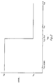
- Figure 2 is a transfer characteristic of the circuit of Figure 1.
- Detection circuit 1 receives as inputs the voltage to be detected and bias voltages.
- the voltage to be detected is the substrate bias voltage V bb , which is received at the source of transistor 2.
- the bias voltages include, in this example, the positive power supply voltage V dd , and a common, or ground, potential V ss .
- the desired potential of the substrate bias V bb is below V ss (for example, at a level on the order of -2.0 volts).
- Detection circuit 1 has an output, on line VBB0, which is at a high logic level when the substrate bias v bb is at a potential above V ss , and is at a low logic level when the substrate bias V bb is below Vss .
- the signal generated by detection circuit 1 on line VBB0 can be used to shut down other circuits on the same integrated circuit chip to avoid such other circuits from entering a latchup state in the absence of sufficient substrate bias.
- n-channel transistor 2 has its source connected to the substrate node V bb .
- the gate of transistor 2 is connected to its drain, and both are connected to the drain of a p-channel transistor 6.
- P-channel transistor 6 has its source connected to V dd , and its gate biased to V ss , and thus presents a pull-up load to transistor 2.
- the drains of transistors 2 and 6 are connected to the gates of n-channel transistor 4 and p-channel transistor 8.
- N-channel transistor 4 and p-channel transistor 8 are connected in inverter fashion, with the source of n-channel transistor 4 biased to V ss .
- the source of p-channel load transistor 8 is biased to V dd , and the drains of transistors 4 and 8 are connected together.
- Inverter 10 has its input connected to the drains of transistors 4 and 8, and its output drives line VBB0, presenting the output of detection circuit 1 with the desired logic scheme (i.e., line VBB0 indicating the absence of sufficient substrate bias with a high logic level).
- Inverter 11 has its input connected to the output of inverter 10, and presents a signal on line VBB0_ which is the logical complement of the signal on line VBB0, and thus indicates loss of V bb with a low logic level.
- V bb at which detection circuit 1 issues a loss-of-V bb signal on line VBB0 be at some level below V ss . This ensures that the remainder of the integrated circuit is disabled well prior to such time as the substrate reaches the voltage at which the base-emitter junction of one of the transistors in the parasitic SCR is forward biased.
- the detection voltage is preferably close to V ss , so that detection circuit 1 will thus only respond to those conditions for which latchup can occur, and will tend not to respond to noise and other transient conditions which can often occur in large scale integrated circuits.
- the level at which detection circuit 1 trips is set in this embodiment by the difference in threshold voltages between transistors 2 and 4.
- transistor 2 to which V bb is connected has a higher threshold voltage than transistor 4, to which V ss is connected.
- the threshold voltage V t2 of transistor 2 can be on the order of +0.8 volts (measured at V bb of -2.0 volts) and the threshold voltage V t4 of transistor 4 can be on the order of +0.5 volts (measured at V bb of -2.0 volts), establishing a difference therebetween on the order of 0.3 volts.
- p-channel load transistor 6 is in the on-state, due to its gate biased to V ss , which biases the gate and drain of transistor 2 into the on-state also. It is preferable that transistor 2 have a much larger width-to-length (W/L) ratio than transistor 6, so that with both transistors in the on-state, the DC current drawn through transistors 2 and 6 is minimal.
- W/L ratio of n-channel transistor 2 may be on the order of 100
- the W/L ratio of p-channel transistor 6 may be on the order of 0.005.
- the voltage at the drains of transistor 2 and 6 will thus be pulled low through transistor 2, until it reaches a level at which transistor 2 turns off. This is approximately at a threshold voltage V t2 above V bb . Accordingly, the voltage at the gates of transistors 4 and 8 is approximately at V bb + V t2 .
- Transistor 8 preferably has a small W/L ratio, compared to transistor 4; for example, transistor 8 may have a W/L ratio on the order of 0.05, with the W/L ratio of transistor 4 on the order of 20. Transistor 4 will, of course, turn on when its gate voltage is at a level greater than its threshold voltage V t4 above V ss .
- transistor 4 Since the voltage at the gate of transistor 4 is at V bb + V t2 , transistor 4 turns on when the following inequality is satisfied: (V bb + V t2 ) - V ss > V t4 which is equivalent to: V bb - V ss > V t4 - V t2
- Figure 2 shows the DC transfer characteristic of substrate bias detection circuit 1 shown in Figure 1.
- V bb bias V bb NOM
- V ss e.g., at -2.0 volts
- line VBB0_ is at a high logic level, indicating adequate substrate bias.
- the trip point of the circuit is at the value V t4 - V t2 , as described above.
- line VBB0_ is at a high logic level; above this voltage, circuit 1 operates to present a low logic level on line VBB0_ at the output of inverter 11.
- the logic state on line VBB0_ at the output of inverter 10 is complementary to the logic state on line VBB0_ shown in Figure 1.
Landscapes
- Engineering & Computer Science (AREA)
- Physics & Mathematics (AREA)
- Microelectronics & Electronic Packaging (AREA)
- Power Engineering (AREA)
- Electromagnetism (AREA)
- Nonlinear Science (AREA)
- General Physics & Mathematics (AREA)
- Radar, Positioning & Navigation (AREA)
- Automation & Control Theory (AREA)
- Computer Hardware Design (AREA)
- Semiconductor Integrated Circuits (AREA)
- Dram (AREA)
- Metal-Oxide And Bipolar Metal-Oxide Semiconductor Integrated Circuits (AREA)
- Testing Or Measuring Of Semiconductors Or The Like (AREA)
- Measurement Of Current Or Voltage (AREA)
Claims (7)
- Circuit de détection de la polarisation d'un substrat du type comprenant un premier transistor (2) ayant sa source connectée à un potentiel de substrat et ayant ses drain et grille couplés à un noeud de commande ; un premier transistor de charge (6) connecté entre lesdits noeuds de commande et potentiel de polarisation; et un deuxième transistor (4) ayant sa source couplée à un potentiel commun, ayant sa grille couplée audit noeud de commande, et ayant un drain, caractérisé en ce qu'il comporte un deuxième transistor de charge (8) connecté en inverse audit deuxième transistor, ledit deuxième transistor de charge étant connecté entre le drain dudit deuxième transistor (4) et ledit potentiel de polarisation, ladite borne de grille dudit deuxième transistor de charge étant couplée audit noeud de commande; et dans lequel ledit premier transistor de charge (6) comporte une borne de grille couplée au potentiel commun.
- Circuit de détection selon la revendication 1, dans lequel lesdits premier et deuxième transistors (2,4) comportent des tensions de seuil différentes.
- Circuit de détection selon la revendication 2, dans lequel la tension de seuil du premier transistor (2) est supérieure à la tension de seuil dudit deuxième transistor (4).
- Circuit de détection selon la revendication 1, comprenant en outre :
un circuit tampon (10) connecté au drain dudit deuxième transistor (4). - Circuit de détection selon la revendication 4, dans lequel ledit circuit tampon (10) comporte un inverseur.
- Circuit de détection selon la revendication 1, dans lequel lesdits premier et deuxième transistors (2,4) sont d'un premier type de conductivité ; et dans lequel ledit premier transistor de charge (6) est d'un deuxième type de conductivité entre ledit noeud de commande et ledit potentiel de polarisation, et ayant sa grille couplée à un potentiel de sorte que le trajet source/-drain est conducteur lorsque ledit premier transistor est conducteur.
- Circuit de détection selon la revendication 1, dans lequel lesdits premier et deuxième transistors (2,4) sont d'un premier type de conductivité ; et dans lequel ledit deuxième transistor de charge (8) est d'un deuxième type de conductivité ayant sa grille couplée à la grille dudit deuxième transistor (4).
Applications Claiming Priority (2)
| Application Number | Priority Date | Filing Date | Title |
|---|---|---|---|
| US47506190A | 1990-02-05 | 1990-02-05 | |
| US475061 | 1999-12-30 |
Publications (3)
| Publication Number | Publication Date |
|---|---|
| EP0441201A2 EP0441201A2 (fr) | 1991-08-14 |
| EP0441201A3 EP0441201A3 (en) | 1992-04-15 |
| EP0441201B1 true EP0441201B1 (fr) | 1996-05-15 |
Family
ID=23886095
Family Applications (1)
| Application Number | Title | Priority Date | Filing Date |
|---|---|---|---|
| EP91100961A Expired - Lifetime EP0441201B1 (fr) | 1990-02-05 | 1991-01-25 | Circuit détecteur de la tension de polarisation du substrat |
Country Status (4)
| Country | Link |
|---|---|
| EP (1) | EP0441201B1 (fr) |
| JP (1) | JP3258675B2 (fr) |
| KR (1) | KR100216435B1 (fr) |
| DE (1) | DE69119439T2 (fr) |
Families Citing this family (2)
| Publication number | Priority date | Publication date | Assignee | Title |
|---|---|---|---|---|
| KR0154167B1 (ko) * | 1994-09-12 | 1998-10-15 | 김영환 | 백 바이어스 검출회로 |
| JPH09213073A (ja) * | 1996-02-06 | 1997-08-15 | Mitsubishi Electric Corp | 半導体集積回路 |
Family Cites Families (4)
| Publication number | Priority date | Publication date | Assignee | Title |
|---|---|---|---|---|
| US4288865A (en) * | 1980-02-06 | 1981-09-08 | Mostek Corporation | Low-power battery backup circuit for semiconductor memory |
| USRE32200E (en) * | 1980-11-03 | 1986-07-08 | Fairchild Semiconductor Corporation | MOS battery backup controller for microcomputer random access memory |
| JPS6238591A (ja) * | 1985-08-14 | 1987-02-19 | Fujitsu Ltd | 相補型の半導体メモリ装置 |
| US4794278A (en) * | 1987-12-30 | 1988-12-27 | Intel Corporation | Stable substrate bias generator for MOS circuits |
-
1991
- 1991-01-25 EP EP91100961A patent/EP0441201B1/fr not_active Expired - Lifetime
- 1991-01-25 DE DE69119439T patent/DE69119439T2/de not_active Expired - Fee Related
- 1991-02-05 JP JP01444491A patent/JP3258675B2/ja not_active Expired - Fee Related
- 1991-02-05 KR KR1019910001963A patent/KR100216435B1/ko not_active Expired - Lifetime
Also Published As
| Publication number | Publication date |
|---|---|
| KR910015862A (ko) | 1991-09-30 |
| EP0441201A3 (en) | 1992-04-15 |
| KR100216435B1 (ko) | 1999-08-16 |
| DE69119439D1 (de) | 1996-06-20 |
| JP3258675B2 (ja) | 2002-02-18 |
| DE69119439T2 (de) | 1996-09-26 |
| EP0441201A2 (fr) | 1991-08-14 |
| JPH07169913A (ja) | 1995-07-04 |
Similar Documents
| Publication | Publication Date | Title |
|---|---|---|
| EP0702860B1 (fr) | Protection contre les surtensions | |
| US5508649A (en) | Voltage level triggered ESD protection circuit | |
| US5568065A (en) | Circuit for connecting a node to a voltage source selected from alternative voltage sources | |
| US5926056A (en) | Voltage tolerant output buffer | |
| US4963766A (en) | Low-voltage CMOS output buffer | |
| US4347447A (en) | Current limiting MOS transistor driver circuit | |
| US5120993A (en) | Substrate bias voltage detection circuit | |
| US20090195269A1 (en) | Input stage for mixed-voltage-tolerant buffer with reduced leakage | |
| US4581551A (en) | Input/output circuit for use with various voltages | |
| US6441651B2 (en) | High voltage tolerable input buffer | |
| US5751179A (en) | Output driver for PCI bus | |
| US6046617A (en) | CMOS level detection circuit with hysteresis having disable/enable function and method | |
| US6064231A (en) | CMOS input buffer protection circuit | |
| JP2959449B2 (ja) | 出力回路 | |
| US6236236B1 (en) | 2.5 volt input/output buffer circuit tolerant to 3.3 and 5 volts | |
| US4296340A (en) | Initializing circuit for MOS integrated circuits | |
| US5432463A (en) | High speed NOR gate with small output voltage swings | |
| EP0441201B1 (fr) | Circuit détecteur de la tension de polarisation du substrat | |
| JP2000029551A (ja) | Cmos基準電圧生成器を含む集積回路 | |
| JP2714380B2 (ja) | Cmos回路および入力線の電圧検出方法. | |
| US6091265A (en) | Low voltage CMOS input buffer with undershoot/overshoot protection | |
| US5952866A (en) | CMOS output buffer protection circuit | |
| US5013935A (en) | CMOS level detctor circuit | |
| KR0129592B1 (ko) | 저잡음 출력 버퍼 | |
| EP0810735A2 (fr) | Tampon à trois états utilisant un transistor bipolaire |
Legal Events
| Date | Code | Title | Description |
|---|---|---|---|
| PUAI | Public reference made under article 153(3) epc to a published international application that has entered the european phase |
Free format text: ORIGINAL CODE: 0009012 |
|
| AK | Designated contracting states |
Kind code of ref document: A2 Designated state(s): DE FR GB IT NL |
|
| PUAL | Search report despatched |
Free format text: ORIGINAL CODE: 0009013 |
|
| AK | Designated contracting states |
Kind code of ref document: A3 Designated state(s): DE FR GB IT NL |
|
| 17P | Request for examination filed |
Effective date: 19921008 |
|
| 17Q | First examination report despatched |
Effective date: 19940609 |
|
| GRAH | Despatch of communication of intention to grant a patent |
Free format text: ORIGINAL CODE: EPIDOS IGRA |
|
| GRAA | (expected) grant |
Free format text: ORIGINAL CODE: 0009210 |
|
| AK | Designated contracting states |
Kind code of ref document: B1 Designated state(s): DE FR GB IT NL |
|
| PG25 | Lapsed in a contracting state [announced via postgrant information from national office to epo] |
Ref country code: NL Free format text: LAPSE BECAUSE OF FAILURE TO SUBMIT A TRANSLATION OF THE DESCRIPTION OR TO PAY THE FEE WITHIN THE PRESCRIBED TIME-LIMIT Effective date: 19960515 |
|
| ITF | It: translation for a ep patent filed | ||
| REF | Corresponds to: |
Ref document number: 69119439 Country of ref document: DE Date of ref document: 19960620 |
|
| ET | Fr: translation filed | ||
| NLV1 | Nl: lapsed or annulled due to failure to fulfill the requirements of art. 29p and 29m of the patents act | ||
| PLBE | No opposition filed within time limit |
Free format text: ORIGINAL CODE: 0009261 |
|
| STAA | Information on the status of an ep patent application or granted ep patent |
Free format text: STATUS: NO OPPOSITION FILED WITHIN TIME LIMIT |
|
| 26N | No opposition filed | ||
| REG | Reference to a national code |
Ref country code: GB Ref legal event code: IF02 |
|
| PGFP | Annual fee paid to national office [announced via postgrant information from national office to epo] |
Ref country code: GB Payment date: 20071212 Year of fee payment: 18 |
|
| PGFP | Annual fee paid to national office [announced via postgrant information from national office to epo] |
Ref country code: DE Payment date: 20080131 Year of fee payment: 18 Ref country code: IT Payment date: 20080116 Year of fee payment: 18 |
|
| PGFP | Annual fee paid to national office [announced via postgrant information from national office to epo] |
Ref country code: FR Payment date: 20080107 Year of fee payment: 18 |
|
| GBPC | Gb: european patent ceased through non-payment of renewal fee |
Effective date: 20090125 |
|
| PG25 | Lapsed in a contracting state [announced via postgrant information from national office to epo] |
Ref country code: DE Free format text: LAPSE BECAUSE OF NON-PAYMENT OF DUE FEES Effective date: 20090801 |
|
| REG | Reference to a national code |
Ref country code: FR Ref legal event code: ST Effective date: 20091030 |
|
| PG25 | Lapsed in a contracting state [announced via postgrant information from national office to epo] |
Ref country code: GB Free format text: LAPSE BECAUSE OF NON-PAYMENT OF DUE FEES Effective date: 20090125 |
|
| PG25 | Lapsed in a contracting state [announced via postgrant information from national office to epo] |
Ref country code: FR Free format text: LAPSE BECAUSE OF NON-PAYMENT OF DUE FEES Effective date: 20090202 |
|
| PG25 | Lapsed in a contracting state [announced via postgrant information from national office to epo] |
Ref country code: IT Free format text: LAPSE BECAUSE OF NON-PAYMENT OF DUE FEES Effective date: 20090125 |