EP0441373B1 - Verfahren und Vorrichtung zur Messung von Musterdimensionen - Google Patents
Verfahren und Vorrichtung zur Messung von Musterdimensionen Download PDFInfo
- Publication number
- EP0441373B1 EP0441373B1 EP91101682A EP91101682A EP0441373B1 EP 0441373 B1 EP0441373 B1 EP 0441373B1 EP 91101682 A EP91101682 A EP 91101682A EP 91101682 A EP91101682 A EP 91101682A EP 0441373 B1 EP0441373 B1 EP 0441373B1
- Authority
- EP
- European Patent Office
- Prior art keywords
- pattern
- inclination angle
- tapered
- measuring portion
- width
- Prior art date
- Legal status (The legal status is an assumption and is not a legal conclusion. Google has not performed a legal analysis and makes no representation as to the accuracy of the status listed.)
- Expired - Lifetime
Links
- 238000000034 method Methods 0.000 title claims description 26
- 238000010894 electron beam technology Methods 0.000 claims description 19
- 238000005259 measurement Methods 0.000 claims description 12
- 238000004364 calculation method Methods 0.000 claims description 9
- 230000003287 optical effect Effects 0.000 claims description 2
- 229910018125 Al-Si Inorganic materials 0.000 description 2
- 229910018520 Al—Si Inorganic materials 0.000 description 2
- 101100042258 Neurospora crassa (strain ATCC 24698 / 74-OR23-1A / CBS 708.71 / DSM 1257 / FGSC 987) sem-1 gene Proteins 0.000 description 2
- 102220538948 SUMO-conjugating enzyme UBC9_F22A_mutation Human genes 0.000 description 2
- 238000005520 cutting process Methods 0.000 description 2
- 239000000463 material Substances 0.000 description 2
- 102220224251 rs1060502313 Human genes 0.000 description 2
- 238000007796 conventional method Methods 0.000 description 1
- 238000001514 detection method Methods 0.000 description 1
- 238000010586 diagram Methods 0.000 description 1
- 238000001914 filtration Methods 0.000 description 1
- 239000012212 insulator Substances 0.000 description 1
- 239000011229 interlayer Substances 0.000 description 1
- 239000010410 layer Substances 0.000 description 1
- 238000004519 manufacturing process Methods 0.000 description 1
- 238000005070 sampling Methods 0.000 description 1
Images


Classifications
-
- G—PHYSICS
- G01—MEASURING; TESTING
- G01B—MEASURING LENGTH, THICKNESS OR SIMILAR LINEAR DIMENSIONS; MEASURING ANGLES; MEASURING AREAS; MEASURING IRREGULARITIES OF SURFACES OR CONTOURS
- G01B11/00—Measuring arrangements characterised by the use of optical techniques
- G01B11/24—Measuring arrangements characterised by the use of optical techniques for measuring contours or curvatures
-
- G—PHYSICS
- G01—MEASURING; TESTING
- G01B—MEASURING LENGTH, THICKNESS OR SIMILAR LINEAR DIMENSIONS; MEASURING ANGLES; MEASURING AREAS; MEASURING IRREGULARITIES OF SURFACES OR CONTOURS
- G01B15/00—Measuring arrangements characterised by the use of electromagnetic waves or particle radiation, e.g. by the use of microwaves, X-rays, gamma rays or electrons
Definitions
- the present invention relates to a method of and an apparatus for measuring a pattern dimension using an electron beam.
- EP-A-0 345 772 discloses a method of and an apparatus for measuring the measuring portion of a pattern of a specimen placed on a rotating specimen stage by controlling a deflector of a scan type electron microscope (SEM) capable of setting a desired inclination angle of one of the specimen stage and a lens barrel, applying an electron beam to the measuring portion of the specimen, and image processing a secondary electron signal from the measuring portion, said method and apparatus comprising: image processing means for processing a secondary electron signal generated from the measuring portion of the specimen placed on said specimen stage upon application of an electron beam to said measuring portion; a computer for calculating the taper angle and depth or height of said pattern and the profile of a taper portion in accordance with an output from said image processing means when said electron beam is applied to said measuring portion at a predetermined inclination angle.
- the electron beam is scanned onto said pattern with said scanning electron microscope in the directions perpendicular and parallel to the longitudinal direction of said pattern.
- the specimen shown in this document may have a "usual" taper, that is a top width (distance of the top edges) which is smaller than the bottom width (distance of the bottom edges), such that the SEM may observe the bottom edges when an electron beam is applied to the object from above.
- US-A-4 725 730 discloses a scanning electron microscope (SEM) for automatically measuring the height and the width of a step-shaped object having a "usual" taper, as defined above.
- SEM scanning electron microscope
- the method and system described in this document comprises the steps of means for detecting the images of the step-shaped object from at least two directions so as to form pictures corresponding to the images detected from different directions, determining the distances between the upper and lower edges of a step in respective pictures; determining the angles of inclination of the edge lines with respect to the axis of the pictures, determining the angles of inclination of the standard plane fixed to the step formed object with respect to the viewing directions, and determining, as significant factors of the shape to be determined, the height and width of the step-shaped object.
- the distance between bottom edges has been determined from the distance between top edges or from the cross section obtained by cutting a specimen, because the bottom edges cannot be observed when a beam is applied vertically.
- An automatic measuring algorithm conventionally used can detect with high precision the distance between bottom edges of a normal taper shape pattern.
- the distance between bottom edges cannot be measured if a beam is applied vertically.
- Manual measurement also allows measurement of only the distance between top edges.
- a reversed taper shape pattern is found, for example, in a negative type electron beam sensitive resist pattern, an Al-Si wiring pattern and the like.
- Al-Si wiring pattern of a reversed taper shape As the distance between adjacent patterns becomes short, the probability of generation of a "blowhole" increases during a manufacturing process for an interlayer insulator film. It is therefore necessary to quantitatively check the degree of reversed taper. It is therefore required to obtain not only the distance between top edges of a reversed taper shape pattern, but also the distance between bottom edges and a difference ratio (dimension reduction ratio) between the top edge and bottom edge distances.
- the distance between top edges of a pattern to be measured is calculated by a first step, and the number of pixels of a taper portion of the pattern is obtained for first and second predetermined inclination angles at second and third steps, respectively.
- the taper angle and height of the pattern are calculated at a fourth step.
- the distance between bottom edges of the pattern to be measured and the difference ratio between the top edge and bottom edge distances are calculated at a fifth step.
- the profile of the taper portion is obtained at a sixth step.
- the cross sectional area of the pattern to be measured is calculated at a seventh step.
- a first calculation means calculates the width or distance between top edges of a pattern to be measured, in accordance with an output from an image processing means when an electron beam is applied at a zero inclination angle.
- a second calculation means calculates the taper angle, height, bottom edge width or distance of the pattern and a dimension reduction ratio between the top edge and bottom edge distances in accordance with an output from the image processing means when an electron beam is applied at first and second predetermined inclination angles.
- a third calculation means calculates the cross sectional area of the pattern. In the above manner, without breaking a specimen, the dimension and cross sectional area of a fine pattern of a reversed taper shape can be correctly measured.
- the dimension and cross sectional area of a fine pattern of a reversed taper shape can be correctly measured without breaking a specimen.
- Fig. 1 shows the structure of a pattern dimension measuring apparatus according to an embodiment of this invention.
- the pattern dimension measuring apparatus of this embodiment is constructed of a scanning electron microscope 1 (hereinafter called an SEM) including an electron optical column 1a, deflector 1b, detector 1c, and stage 1d for holding a specimen 10, an image processing means 2 for receiving a video signal from the detector 1c and performing various image processing, a computer 3 for controlling the image processing means and the stage and for performing calculations for measurement of dimensions and shapes, an image monitor 4, and a stage controller 5.
- SEM scanning electron microscope
- Figs. 2 to 5 The structure and operation of this embodiment will be described with reference to Figs. 2 to 5 by taking as an example the case where a pattern of a reversed taper shape shown in Fig. 7 is measured.
- the pattern shown in Fig. 7 is assumed that the right and left of the cross section thereof are symmetrical relative to the central axis.
- the image processing means 2 sends deflection control signals for SEM 1 to the deflector 1b to thereby scan the electron beam, the deflection control signals including an Horizontal Scan (HS) signal, Vertical Scan (VS) signal, Horizontal Blank (HB) signal, Vertical Blank (VB) signal, and Control (CONT) signal (step F22A).
- the deflection control signals including an Horizontal Scan (HS) signal, Vertical Scan (VS) signal, Horizontal Blank (HB) signal, Vertical Blank (VB) signal, and Control (CONT) signal (step F22A).
- a detection output (secondary electron signal) from the detector 1c is sent to the image processing means 2 whereat it is sampled at a predetermined sampling timing and A/D converted (step F22B), and thereafter subjected to a mean addition process, a spatial filtering process and a linear image emphasizing process, the processed results being stored in a frame memory of the image processing means 2 having 256 tonal steps, and the signal waveforms being displayed on the image monitor 4 (step F22C).
- the processes from the step F22A to F22C are collectively called an image data input process hereinafter where applicable.
- the signal waveforms thus obtained and shown in Fig. 3
- the top portion width or distance L T is calculated by the computer 3 (step F23).
- the inclination angle ⁇ of the stage 1d of SEM 1 is set to a predetermined inclination angle ⁇ 1 to allow observing the bottom edges (step F24), and thereafter, the above-described image input process is executed (step F25).
- the number P1 of pixels corresponding to the taper portion width of the pattern is obtained (step F26).
- the inclination angle ⁇ of the stage 1d is set to a predetermined inclination angle ⁇ 2 (different from ⁇ 1) to allow observing the bottom edges (step F27), and thereafter the similar image input process is executed (step F28).
- step F29 the number P2 of pixels corresponding to the same taper portion width is obtained (step F29).
- the taper angle ⁇ , and height H (film thickness) are calculated by the computer 3 using the following equations (1) and (2) derived from the stereoscopic principle (step F30): where M represents a measurement magnification, and C represents a length on the image monitor 4 of one pixel at the measurement magnification M.
- the distance X (h i ) from the bottom edge at the height h i can be obtained.
- the cross sectional area S of the pattern is therefore calculated using the following equation (8) (step F34): where ⁇ h represents the increment of height per one pixel at the height h i .
- the measurement results of a pattern of a reversed taper shape obtained using the pattern dimension measuring apparatus of this embodiment are shown in Fig. 6.
- the rotating stage After determining the taper shape at one side using the first and second predetermined angle, the stage is inclined in the opposite angular direction to obtain third and fourth predetermined inclination angles ⁇ 3 and ⁇ 4.
- these angles are selected under the condition that they allow observing the bottom edges.
- the tape shape (height, taper angle, profile and so on) at the other side is calculated using the angles ⁇ 3 and ⁇ 4, and the number of pixels P3 and P4 obtained by the same method as described above. Then the bottom dimension is calculated using the taper shapes at both sides and the top dimension.
- the stage is roated after obtaining P1 at the first predetermined inclination angle ⁇ 1. If the bottom edge can be observed after rotating the stage for 180 degrees, there is no need to change the inclination angle of the stage, and the third predetermined inclination angle ⁇ 3 at this time is the same as the first predetermined inclination angle ⁇ 1. Similarly, the fourth predetermined inclination angle ⁇ 4 can be selected the same as the second predetermined inclination angle ⁇ 2 by rotating the stage.
Landscapes
- Physics & Mathematics (AREA)
- General Physics & Mathematics (AREA)
- Electromagnetism (AREA)
- Length-Measuring Devices Using Wave Or Particle Radiation (AREA)
Claims (5)
- Musterabmessungsmeßverfahren zur Messung der Abmessungen eines Musters mit umgekehrter Verjüngung einer Probe (10), wobei das Muster mit umgekehrter Verjüngung eine größere obere Breite (LT) und eine kleinere untere Breite (LB) aufweist, so daß die Bodenkanten des Musters nicht in Vertikalrichtung von oben beobachtet werden können, wobei das Muster auf eine Probenstufe (1d) aufgesetzt ist, durch Steuern einer Ablenkvorrichtung (1b) eines Lasterelektronenmikroskops (1), welches einen Neigungswinkel (ϑ) zwischen der Probenstufe (1d) und einem Objektivtubus (1a) einstellen kann, einen Elektronenstrahl an einen Meßabschnitt der Probe (10) anlegen kann, und eine Bildbearbeitung eines Sekundärelektronensignals von dem Meßabschnitt durchführen kann, wobei das Verfahren aufweist:
einen ersten Schritt der Berechnung der Breite (LT) zwischen den Oberkanten des Meßabschnitts des Musters mit umgekehrter Verjüngung durch Bildbearbeitung des Sekundärelektronensignals, wenn der Elektronenstrahl auf den Meßabschnitt in einem Neigungswinkel (ϑ) von Null aufgebracht wird;
einen zweiten Schritt, bei welchem die Anzahl an Pixeln (P₁) in einer verjüngten Seitenwand des Meßabschnitts des Musters mit umgekehrter Verjüngung erhalten wird, durch Bildbearbeitung des Sekundärelektronensignals, wenn der Elektronenstrahl auf den Meßabschnitt in einem ersten vorbestimmten Neigungswinkel (ϑ₁) aufgebracht wird, der eine Beobachtung der Bodenkanten gestattet;
einen dritten Schritt, bei welchem die Anzahl an Pixeln (P₂) an der verjüngten Seitenwand durch Bildbearbeitung des Sekundärelektronenstrahls erhalten wird, wenn der Elektronenstrahl auf den Meßabschnitt in einem zweiten vorbestimmten Neigungswinkel (ϑ₂) aufgebracht wird, der sich von dem ersten Neigungswinkel (ϑ₁) unterscheidet und ebenfalls eine Beobachtung der Bodenkanten gestattet;
einen vierten Schritt der Berechnung eines Winkels φ der verjüngten Seitenwand und der Höhe (H) des Musters entsprechend der Anzahl an Pixeln (P₁, P₂) der verjüngten Seitenwand, die in dem zweiten und dritten Schritt und bei dem ersten und zweiten vorbestimmten Neigungswinkel (ϑ₁, ϑ₂) erhalten werden; und
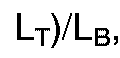
einen fünften Schritt der Berechnung der Breite (LB) zwischen den Bodenkanten des Musters mit umgekehrter Verjüngung, und der Berechnung eines Abmessungsverringerungsverhältnisses
- Verfahren nach Anspruch 1, bei welchem weiterhin ein sechster Schritt vorgesehen ist, bei welchem dann, wenn der Verjüngungsabschnitt des Musters nicht durch eine gerade Linie approximiert werden kann, das Profil des Verjüngungsabschnitts als Kontur der verjüngten Wand entsprechend der Stärkeänderung des Sekundärelektronensignals von dem verjüngten Abschnitt erhalten wird.
- Verfahren nach Anspruch 1, bei welchem dann, wenn die Winkel der verjüngten Seitenwände an der rechten und linken Seite des Musters unterschiedlich sind, nach einer ersten Abmessungsmessung an einer Seite unter Verwendung des ersten vorbestimmten Neigungswinkels (ϑ₁) und des zweiten vorbestimmten Neigungswinkels (ϑ₂), eine zweite Abmessungsmessung an der anderen Seite durchgeführt wird, unter Verwendung eines dritten vorbestimmten Neigungswinkels (ϑ₃) und eines vierten Neigungswinkels (ϑ₄), welche durch Drehung einer Drehstufe oder Änderung des Stufenwinkels in entgegengesetzter Winkelrichtung erhalten werden.
- Verfahren nach Anspruch 2, bei welchem weiterhin ein siebter Schritt der Berechnung der Querschnittsfläche (S) des Meßabschnitts des Musters entsprechend der Bodenbreite (LB) und der Kontur der verjüngten Wand vorgesehen ist, die in dem fünften bzw. sechsten Schritt erhalten werden.
- Abmessungsmeßvorrichtung für ein Muster mit umgekehrter Verjüngung, mit:
einem Rasterelektronenmikroskop (1), welches einen Neigungswinkel (ϑ) durch Bewegung zumindest entweder einer Probenstufe (1d) zur Aufbringung einer Probe (10) oder einer Elektronenoptiksäule (1a) einstellen kann;
einer Bildbearbeitungsvorrichtung (2) zur Bearbeitung eines Sekundärelektronensignals, welches von dem Meßabschnitt der Probe (10) erzeugt wird, die auf die Probenstufe (1d) aufgesetzt ist, nach Anlegen eines Elektronenstrahls an den Meßabschnitt;
einer ersten Berechnungsvorrichtung (3) zur Berechnung der Breite (LT) zwischen den Oberkanten des Meßabschnitts des Musters mit umgekehrter Verjüngung entsprechend einem Ausgangssignal von der Bildbearbeitungsvorrichtung (2), wenn der Elektronenstrahl an den Meßabschnitt in einem Neigungswinkel (ϑ) von Null angelegt wird;
einer zweiten Berechnungsvorrichtung (3) zur Berechnung eines Winkels (φ) einer verjüngten Seitenwand, der Höhe (H) des Musters mit umgekehrter Verjüngung, der Breite (LB) zwischen den Bodenkanten des Musters, eines Verhältnisses (F) einer Differenz (LB-LT) der oberen Kantenentfernung und der unteren Kantenentfernung (LT, LB) und der Bodenbreite (LB), und einer Kontur der verjüngten Wand entsprechend Ausgangssignalen von der Bearbeitungsvorrichtung, wenn der Elektronenstrahl auf den Meßabschnitt in einem ersten Neigungswinkel (ϑ₁) und einem zweiten Neigungswinkel (ϑ₂) aufgebracht wird, wobei beide Neigungswinkel (ϑ₁, ϑ₂) eine Beobachtung der Bodenkanten des Musters mit umgekehrter Verjüngung gestatten und voneinander unterschiedliche Werte aufweisen; und
einer dritten Berechnungsvorrichtung (3) zur Berechnung der Oberflächenfläche (S) des Musters entsprechend den Ausgangssignalen von der zweiten Berechnungsvorrichtung (3).
Applications Claiming Priority (2)
| Application Number | Priority Date | Filing Date | Title |
|---|---|---|---|
| JP28013/90 | 1990-02-07 | ||
| JP2028013A JPH07111336B2 (ja) | 1990-02-07 | 1990-02-07 | パターン寸法測定方法及び装置 |
Publications (3)
| Publication Number | Publication Date |
|---|---|
| EP0441373A2 EP0441373A2 (de) | 1991-08-14 |
| EP0441373A3 EP0441373A3 (en) | 1992-12-16 |
| EP0441373B1 true EP0441373B1 (de) | 1995-08-16 |
Family
ID=12236892
Family Applications (1)
| Application Number | Title | Priority Date | Filing Date |
|---|---|---|---|
| EP91101682A Expired - Lifetime EP0441373B1 (de) | 1990-02-07 | 1991-02-07 | Verfahren und Vorrichtung zur Messung von Musterdimensionen |
Country Status (5)
| Country | Link |
|---|---|
| US (1) | US5159643A (de) |
| EP (1) | EP0441373B1 (de) |
| JP (1) | JPH07111336B2 (de) |
| KR (1) | KR940007113B1 (de) |
| DE (1) | DE69112090T2 (de) |
Families Citing this family (21)
| Publication number | Priority date | Publication date | Assignee | Title |
|---|---|---|---|---|
| US5398307A (en) * | 1990-07-06 | 1995-03-14 | Matsushita Electric Industrial Co., Ltd. | Mesh generating method and apparatus therefor |
| JP2823450B2 (ja) * | 1992-11-19 | 1998-11-11 | 株式会社東芝 | 回路パターンの寸法測定方法 |
| US5541411A (en) * | 1995-07-06 | 1996-07-30 | Fei Company | Image-to-image registration focused ion beam system |
| US6075859A (en) * | 1997-03-11 | 2000-06-13 | Qualcomm Incorporated | Method and apparatus for encrypting data in a wireless communication system |
| GB2344182A (en) * | 1997-09-03 | 2000-05-31 | Great Dividers Manufacturing C | Measuring instrument and combination measuring instrument and costing program |
| US6104493A (en) * | 1998-05-14 | 2000-08-15 | Fujitsu Limited | Method and apparatus for visual inspection of bump array |
| US6326618B1 (en) * | 1999-07-02 | 2001-12-04 | Agere Systems Guardian Corp. | Method of analyzing semiconductor surface with patterned feature using line width metrology |
| JP4767650B2 (ja) * | 1999-11-05 | 2011-09-07 | 株式会社トプコン | 半導体デバイス検査装置 |
| US6670612B1 (en) * | 2002-07-01 | 2003-12-30 | Kla-Tencor Technologies Corporation | Undercut measurement using SEM |
| KR101057554B1 (ko) * | 2002-07-11 | 2011-08-17 | 어플라이드 머티리얼즈 이스라엘 리미티드 | 입자빔으로 임계 치수를 측정하기 위한 방법 및 장치 |
| KR101035426B1 (ko) * | 2003-07-11 | 2011-05-18 | 어플라이드 머티리얼즈 이스라엘 리미티드 | 기준 구조 엘리먼트를 이용하여 구조 엘리먼트의 단면 피쳐를 결정하는 시스템 및 방법 |
| JP2007201660A (ja) * | 2006-01-25 | 2007-08-09 | Fuji Xerox Co Ltd | 画像処理装置、画像形成装置、画像処理方法及びプログラム |
| JP4546500B2 (ja) * | 2007-04-04 | 2010-09-15 | 株式会社日立ハイテクノロジーズ | パターン計測方法及びパターン計測装置、並びにパターン工程制御方法 |
| US8059918B2 (en) * | 2008-10-12 | 2011-11-15 | Fei Company | High accuracy beam placement for local area navigation |
| US8781219B2 (en) | 2008-10-12 | 2014-07-15 | Fei Company | High accuracy beam placement for local area navigation |
| JP5254099B2 (ja) * | 2009-03-23 | 2013-08-07 | 株式会社ニューフレアテクノロジー | パターン寸法測定方法及び荷電粒子ビーム描画方法 |
| CN102096307A (zh) * | 2009-12-14 | 2011-06-15 | 鸿富锦精密工业(深圳)有限公司 | 测试相机镜头偏转角度的方法和装置 |
| EP2612342B1 (de) | 2010-08-31 | 2018-08-22 | FEI Company | Navigation und probenbearbeitung unter verwendung einer ionenquelle mit sowohl massearmen als auch massereichen spezies |
| JP6061496B2 (ja) * | 2012-05-21 | 2017-01-18 | 株式会社日立ハイテクノロジーズ | パターン計測装置、パターン計測方法及びパターン計測プログラム |
| CN103196400A (zh) * | 2013-04-08 | 2013-07-10 | 常州同泰光电有限公司 | 一种量测图案化衬底的量测方法 |
| CN105158050B (zh) * | 2015-08-12 | 2019-07-30 | 核工业理化工程研究院 | 一种用于纤维扫描电镜试验的固定装置与试验方法 |
Family Cites Families (7)
| Publication number | Priority date | Publication date | Assignee | Title |
|---|---|---|---|---|
| US4326252A (en) * | 1976-11-29 | 1982-04-20 | Hitachi Medical Corporation | Method of reconstructing cross-section image |
| US4406545A (en) * | 1981-05-07 | 1983-09-27 | Western Electric Company, Inc. | Methods of and apparatus for measuring surface areas |
| JPS6161002A (ja) * | 1984-09-03 | 1986-03-28 | Hitachi Ltd | 断面形状自動測定方式 |
| DE3580647D1 (de) * | 1984-09-19 | 1991-01-03 | Ishida Scale Mfg Co Ltd | Verfahren zum bestimmen eines volumens. |
| JPS61128114A (ja) * | 1984-11-27 | 1986-06-16 | Toshiba Corp | パタ−ンの表面形状評価方法 |
| JPH0621784B2 (ja) * | 1984-12-10 | 1994-03-23 | 株式会社日立製作所 | パタ−ン形状評価装置 |
| JPH01311551A (ja) * | 1988-06-08 | 1989-12-15 | Toshiba Corp | パターン形状測定装置 |
-
1990
- 1990-02-07 JP JP2028013A patent/JPH07111336B2/ja not_active Expired - Lifetime
-
1991
- 1991-02-07 KR KR1019910002058A patent/KR940007113B1/ko not_active Expired - Fee Related
- 1991-02-07 DE DE69112090T patent/DE69112090T2/de not_active Expired - Fee Related
- 1991-02-07 EP EP91101682A patent/EP0441373B1/de not_active Expired - Lifetime
- 1991-02-07 US US07/651,795 patent/US5159643A/en not_active Expired - Lifetime
Also Published As
| Publication number | Publication date |
|---|---|
| JPH07111336B2 (ja) | 1995-11-29 |
| DE69112090D1 (de) | 1995-09-21 |
| KR940007113B1 (ko) | 1994-08-05 |
| EP0441373A2 (de) | 1991-08-14 |
| US5159643A (en) | 1992-10-27 |
| KR910015840A (ko) | 1991-09-30 |
| JPH03233310A (ja) | 1991-10-17 |
| DE69112090T2 (de) | 1996-05-09 |
| EP0441373A3 (en) | 1992-12-16 |
Similar Documents
| Publication | Publication Date | Title |
|---|---|---|
| EP0441373B1 (de) | Verfahren und Vorrichtung zur Messung von Musterdimensionen | |
| EP0345772B1 (de) | Apparat zum Messen einer Musterkonfiguration | |
| EP0641021B1 (de) | Teilchenanalyse von gekerbten Scheiben | |
| US6587581B1 (en) | Visual inspection method and apparatus therefor | |
| EP0319797B1 (de) | Verfahren und Vorrichtung zur Messung der Fehlerdichte und -verteilung | |
| US5161201A (en) | Method of and apparatus for measuring pattern profile | |
| US6208417B1 (en) | Method and apparatus for detecting minute irregularities on the surface of an object | |
| EP0312083B1 (de) | Konturenmessmethode | |
| EP1276134B1 (de) | Verfahren zur Bestimmung von Vertiefungen und Erhebungen in einer Probe und Ladungsträgerteilchenstrahlgerät zur Implementierung dieses Verfahrens | |
| EP0781976A2 (de) | Messverfahren einer kritischen Dimension eines Musters auf einer Probe | |
| US4733074A (en) | Sample surface structure measuring method | |
| US4725730A (en) | System of automatically measuring sectional shape | |
| US7274820B2 (en) | Pattern evaluation system, pattern evaluation method and program | |
| US5555319A (en) | Critical dimension measuring method and equipment thereof | |
| JP2535695B2 (ja) | 走査型電子顕微鏡の自動焦点合わせ方法 | |
| US6295384B1 (en) | Removing noise caused by artifacts from a digital image signal | |
| US6163374A (en) | Bending angle detection system | |
| JPH05187825A (ja) | 異形棒鋼の形状計測方法及び装置 | |
| US6455832B1 (en) | Defect discriminating method and device for solid-state detector | |
| JP2961140B2 (ja) | 画像処理方法 | |
| JP2965370B2 (ja) | 欠陥検出装置 | |
| JPH06103950A (ja) | 走査電子顕微鏡における立体像取得方法 | |
| JPH09101124A (ja) | 穴の面取り量検査方法 | |
| Van De Stadt et al. | Fast 3-D integrated ciruit inspection | |
| JPH03289507A (ja) | パターン寸法測定方法及び装置 |
Legal Events
| Date | Code | Title | Description |
|---|---|---|---|
| PUAI | Public reference made under article 153(3) epc to a published international application that has entered the european phase |
Free format text: ORIGINAL CODE: 0009012 |
|
| 17P | Request for examination filed |
Effective date: 19910207 |
|
| AK | Designated contracting states |
Kind code of ref document: A2 Designated state(s): DE FR GB |
|
| PUAL | Search report despatched |
Free format text: ORIGINAL CODE: 0009013 |
|
| AK | Designated contracting states |
Kind code of ref document: A3 Designated state(s): DE FR GB |
|
| RHK1 | Main classification (correction) |
Ipc: G01B 15/04 |
|
| 17Q | First examination report despatched |
Effective date: 19940216 |
|
| GRAA | (expected) grant |
Free format text: ORIGINAL CODE: 0009210 |
|
| AK | Designated contracting states |
Kind code of ref document: B1 Designated state(s): DE FR GB |
|
| REF | Corresponds to: |
Ref document number: 69112090 Country of ref document: DE Date of ref document: 19950921 |
|
| ET | Fr: translation filed | ||
| PLBE | No opposition filed within time limit |
Free format text: ORIGINAL CODE: 0009261 |
|
| STAA | Information on the status of an ep patent application or granted ep patent |
Free format text: STATUS: NO OPPOSITION FILED WITHIN TIME LIMIT |
|
| 26N | No opposition filed | ||
| REG | Reference to a national code |
Ref country code: GB Ref legal event code: 746 Effective date: 19981007 |
|
| REG | Reference to a national code |
Ref country code: FR Ref legal event code: D6 |
|
| REG | Reference to a national code |
Ref country code: GB Ref legal event code: IF02 |
|
| PGFP | Annual fee paid to national office [announced via postgrant information from national office to epo] |
Ref country code: DE Payment date: 20070201 Year of fee payment: 17 |
|
| PGFP | Annual fee paid to national office [announced via postgrant information from national office to epo] |
Ref country code: GB Payment date: 20070207 Year of fee payment: 17 |
|
| PGFP | Annual fee paid to national office [announced via postgrant information from national office to epo] |
Ref country code: FR Payment date: 20070208 Year of fee payment: 17 |
|
| GBPC | Gb: european patent ceased through non-payment of renewal fee |
Effective date: 20080207 |
|
| REG | Reference to a national code |
Ref country code: FR Ref legal event code: ST Effective date: 20081031 |
|
| PG25 | Lapsed in a contracting state [announced via postgrant information from national office to epo] |
Ref country code: DE Free format text: LAPSE BECAUSE OF NON-PAYMENT OF DUE FEES Effective date: 20080902 |
|
| PG25 | Lapsed in a contracting state [announced via postgrant information from national office to epo] |
Ref country code: FR Free format text: LAPSE BECAUSE OF NON-PAYMENT OF DUE FEES Effective date: 20080229 |
|
| PG25 | Lapsed in a contracting state [announced via postgrant information from national office to epo] |
Ref country code: GB Free format text: LAPSE BECAUSE OF NON-PAYMENT OF DUE FEES Effective date: 20080207 |