EP0441715A1 - Elektrisches Schaltkreis-Bauelement aus einem Supraleitungsmaterial 2. Art - Google Patents
Elektrisches Schaltkreis-Bauelement aus einem Supraleitungsmaterial 2. Art Download PDFInfo
- Publication number
- EP0441715A1 EP0441715A1 EP91420002A EP91420002A EP0441715A1 EP 0441715 A1 EP0441715 A1 EP 0441715A1 EP 91420002 A EP91420002 A EP 91420002A EP 91420002 A EP91420002 A EP 91420002A EP 0441715 A1 EP0441715 A1 EP 0441715A1
- Authority
- EP
- European Patent Office
- Prior art keywords
- superconductive
- axis
- contacts
- type
- magnetization
- Prior art date
- Legal status (The legal status is an assumption and is not a legal conclusion. Google has not performed a legal analysis and makes no representation as to the accuracy of the status listed.)
- Withdrawn
Links
- 239000000463 material Substances 0.000 title claims abstract description 22
- 230000002441 reversible effect Effects 0.000 claims abstract description 9
- 230000005415 magnetization Effects 0.000 claims description 22
- 239000000758 substrate Substances 0.000 claims description 2
- 230000015572 biosynthetic process Effects 0.000 claims 1
- 238000000151 deposition Methods 0.000 claims 1
- 230000008021 deposition Effects 0.000 claims 1
- 238000000427 thin-film deposition Methods 0.000 claims 1
- 239000002887 superconductor Substances 0.000 description 26
- 230000002427 irreversible effect Effects 0.000 description 5
- 239000013078 crystal Substances 0.000 description 4
- 230000003071 parasitic effect Effects 0.000 description 2
- 229910003098 YBa2Cu3O7−x Inorganic materials 0.000 description 1
- 150000001875 compounds Chemical class 0.000 description 1
- 230000007423 decrease Effects 0.000 description 1
- 238000010030 laminating Methods 0.000 description 1
- 229910052761 rare earth metal Inorganic materials 0.000 description 1
- 150000002910 rare earth metals Chemical class 0.000 description 1
- 239000010409 thin film Substances 0.000 description 1
- 230000007704 transition Effects 0.000 description 1
- 229910021521 yttrium barium copper oxide Inorganic materials 0.000 description 1
Images


Classifications
-
- H—ELECTRICITY
- H10—SEMICONDUCTOR DEVICES; ELECTRIC SOLID-STATE DEVICES NOT OTHERWISE PROVIDED FOR
- H10N—ELECTRIC SOLID-STATE DEVICES NOT OTHERWISE PROVIDED FOR
- H10N60/00—Superconducting devices
- H10N60/80—Constructional details
- H10N60/85—Superconducting active materials
- H10N60/855—Ceramic superconductors
- H10N60/857—Ceramic superconductors comprising copper oxide
-
- H—ELECTRICITY
- H10—SEMICONDUCTOR DEVICES; ELECTRIC SOLID-STATE DEVICES NOT OTHERWISE PROVIDED FOR
- H10N—ELECTRIC SOLID-STATE DEVICES NOT OTHERWISE PROVIDED FOR
- H10N60/00—Superconducting devices
- H10N60/01—Manufacture or treatment
- H10N60/0268—Manufacture or treatment of devices comprising copper oxide
- H10N60/0744—Manufacture or deposition of electrodes
Definitions
- the present invention relates to the field of producing electrical circuits of type 2 superconductive material which will be the only superconductors considered here.
- the present invention based on a new analysis of the phenomena appearing in type 2 superconductors, proposes a mode of connection of a superconductor making it possible to obtain a high critical current beyond the H * field from which the cycle magnetization becomes reversible.
- Type 2 superconductive materials prepared in the form of thin layers or crystals are generally in the form of platelets whose thickness along the axis c is very small and whose dimensions in the planes (a, b) are large.
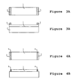
- FIGS. 3A and 3B illustrate the conventional connection mode of a superconductor 1 deposited in a thin layer on a substrate 2.
- the axis c is perpendicular to the plane of the thin layer.
- the contacts 3 and 4 at the ends of the superconductive layer are deposited on the largest surface, that is to say parallel to the planes (a, b), as this naturally results from the geometry of the materials prepared. This also corresponds to the wish to obtain a contact resistance as low as possible.
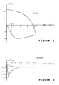
- magnetization cycles illustrated in FIGS. 1 and 2 correspond to fields applied along the axis c, that is to say orthogonally to the plane of the superconductor 1.
- the phenomenon of appearance of the reversibility of the magnetization cycle beyond an H * field, as illustrated in FIG. 2 is an anisotropic phenomenon.
- the irreversibility limit field H * (which varies with temperature) corresponds to a real phase transition which marks the appearance of a laminated superconductive structure in which the superconductive layer 1 is divided into sheets parallel to the planes (a, b ), these sheets being alternately superconductive and with finite conductivity corresponding to the normal state.
- H * which varies with temperature
- the applicant has shown, in the case of YBa2Cu3O7 crystals, that the critical current density increases when the thickness of the crystals decreases. This variation is inversely proportional to the thickness, as shown in Figure 5.
- the more the material becomes laminated the more the critical current density increases to reach the critical limit current of the superconductor.
- the superconductive materials known to contain, parallel to the planes (a, b), intergrowths of parasitic phase sheets (this parasitic phase being at normal conductivity or having a low critical temperature) or of the same phase but with a great deal of disorder atomic will contain weak superconductive bonds which the magnetic field will easily make normal.
- the present invention provides, on the one hand, as has been stated above, to suitably arrange the contacts at the ends of a superconducting circuit element, in a manner substantially transverse to the direction towards which the superconductor extends from of the contact and, on the other hand, to leaf as far as possible along the planes (a, b) the critallographic structure.
- Laminating can be carried out by associating in parallel sheets of material oriented along the planes (a, b) of the crystallographic structure, for example by using super-networks of sheets of Bi2Sr2Ca2Cu3O3 of thickness less than 10 micrometers separated by d ' other sheets of the compound Bi2Sr3CuO6 or Bi2Sr2Ca 2-x Y x Cu3O 10 + y where Y can be replaced by another rare earth in sufficient concentration to make the conductivity of this sheet disappear.
- Bi2Sr2Ca2Cu3O10 whose critical temperature is of the order of 110 K always contains, under non-stoichiometric conditions, minority phases such as Bi2Sr2CaCu2O8 and Bi2Sr2CuO6 which have lower critical temperatures.
- This also constitutes an original aspect of the present invention since it was generally considered in the prior art that the existence of such intergrowth sheets was a source of weak bonds harmful to superconductivity.
- the superconductive element to which the invention will apply will be a component of an electrical circuit, for example a turn or a line which it is desired to connect to other components of the circuit.
- the present invention has been described essentially in the context of thin film superconductors. It will also apply to monocrystalline or texture oriented superconductors in the form of wires, bars, or the like.
- FIG. 6A represents magnetization cycles for fields of 1 and 2 teslas, as a function of the temperature between 2 and 8 K. It can be seen that, as soon as the field reaches approximately 2 T, the magnetization cycle becomes reversible.
- FIG. 6B represents, for the material of FIG. 6a, the critical current density at 4.2 ° K as a function of the field applied. At this temperature, the magnetization curve is reversible as soon as the field reaches about 1 T and yet the critical current density is far from negligible beyond this value.
Landscapes
- Engineering & Computer Science (AREA)
- Manufacturing & Machinery (AREA)
- Chemical & Material Sciences (AREA)
- Ceramic Engineering (AREA)
- Superconductors And Manufacturing Methods Therefor (AREA)
- Containers, Films, And Cooling For Superconductive Devices (AREA)
Applications Claiming Priority (2)
| Application Number | Priority Date | Filing Date | Title |
|---|---|---|---|
| FR9000366A FR2656956B1 (fr) | 1990-01-05 | 1990-01-05 | Element de circuit electrique en materiau supraconducteur de type 2. |
| FR9000366 | 1990-01-05 |
Publications (1)
| Publication Number | Publication Date |
|---|---|
| EP0441715A1 true EP0441715A1 (de) | 1991-08-14 |
Family
ID=9392744
Family Applications (1)
| Application Number | Title | Priority Date | Filing Date |
|---|---|---|---|
| EP91420002A Withdrawn EP0441715A1 (de) | 1990-01-05 | 1991-01-04 | Elektrisches Schaltkreis-Bauelement aus einem Supraleitungsmaterial 2. Art |
Country Status (2)
| Country | Link |
|---|---|
| EP (1) | EP0441715A1 (de) |
| FR (1) | FR2656956B1 (de) |
Cited By (1)
| Publication number | Priority date | Publication date | Assignee | Title |
|---|---|---|---|---|
| EP0729192A1 (de) * | 1995-02-20 | 1996-08-28 | Sumitomo Electric Industries, Ltd. | Metallelektrode für supraleitenden Strompfad in oxidischem Supraleiter und diese verwendende supraleitende Anordnung |
Citations (3)
| Publication number | Priority date | Publication date | Assignee | Title |
|---|---|---|---|---|
| EP0280308A2 (de) * | 1987-02-27 | 1988-08-31 | Hitachi, Ltd. | Supraleiter-Bauelement |
| EP0292436A2 (de) * | 1987-05-18 | 1988-11-23 | International Business Machines Corporation | Leiter mit hohem Strom und Hochfeldmagnete mit anisotropischen Supraleitern |
| EP0302354A2 (de) * | 1987-08-05 | 1989-02-08 | Siemens Aktiengesellschaft | Verfahren zur Herstellung eines schichtartigen Aufbaus aus einem oxidkeramischen Supraleitermaterial |
-
1990
- 1990-01-05 FR FR9000366A patent/FR2656956B1/fr not_active Expired - Fee Related
-
1991
- 1991-01-04 EP EP91420002A patent/EP0441715A1/de not_active Withdrawn
Patent Citations (3)
| Publication number | Priority date | Publication date | Assignee | Title |
|---|---|---|---|---|
| EP0280308A2 (de) * | 1987-02-27 | 1988-08-31 | Hitachi, Ltd. | Supraleiter-Bauelement |
| EP0292436A2 (de) * | 1987-05-18 | 1988-11-23 | International Business Machines Corporation | Leiter mit hohem Strom und Hochfeldmagnete mit anisotropischen Supraleitern |
| EP0302354A2 (de) * | 1987-08-05 | 1989-02-08 | Siemens Aktiengesellschaft | Verfahren zur Herstellung eines schichtartigen Aufbaus aus einem oxidkeramischen Supraleitermaterial |
Non-Patent Citations (2)
| Title |
|---|
| LETTERS TO NATURE vol. 342, 2 novembre 1989, pages 55-57; R.B VAN DOVER et al.: "Critical currents near 10 6 A cm -2 at 77 K in neutron-irradiated single-crystal YBa2Cu3O7" * |
| PROCEEDINGS OF THE IEEE vol. 77, no. 8, août 1989, pages 1124-1130, New York, US; K. TACHIKAWA et al.: "Potential Methods for the Fabrication of High-Tc Superconductors for Wires and Cables" * |
Cited By (1)
| Publication number | Priority date | Publication date | Assignee | Title |
|---|---|---|---|---|
| EP0729192A1 (de) * | 1995-02-20 | 1996-08-28 | Sumitomo Electric Industries, Ltd. | Metallelektrode für supraleitenden Strompfad in oxidischem Supraleiter und diese verwendende supraleitende Anordnung |
Also Published As
| Publication number | Publication date |
|---|---|
| FR2656956B1 (fr) | 1997-01-24 |
| FR2656956A1 (fr) | 1991-07-12 |
Similar Documents
| Publication | Publication Date | Title |
|---|---|---|
| EP1225593B1 (de) | Magnetische Anordnung basiert auf Spinpolarisierung und Rotationsmagnetisierung, Speicher und Schreibverfahren unter Verwendung einer solcher | |
| FR2500333A1 (de) | ||
| EP0284495B1 (de) | Magnetkopf zum Lesen von Spuren mit sehr schmaler Breite und Herstellungverfahren | |
| EP0853766A1 (de) | Magnetfeldsensor mit einer magnetowiderstandsbrücke | |
| EP1031844A2 (de) | Verfahren zur Herstellung eines elektrischen Stromsensors | |
| EP0511056A1 (de) | Josephsonjunctionstruktur | |
| FR2595479A1 (fr) | Element de commutation de lumiere magneto-optique et son procede de fabrication | |
| FR2568419A1 (fr) | Microconnecteur a haute densite de contacts. | |
| EP0240435B1 (de) | Integrierter Widerstand auf einem Halbleitersubstrat | |
| EP0392944A1 (de) | Hochspannungs-Spiralwiderstand | |
| EP2517352A1 (de) | Magnetoresistiver hf-oszillator | |
| EP0191668A1 (de) | Keramischer Hochfrequenzmehrschichtkondensator mit hoher Kapazität | |
| FR2656956A1 (fr) | Element de circuit electrique en materiau supraconducteur de type 2. | |
| EP1419506B1 (de) | Steuereinrichtung zur umkehr der magnetisierungsrichtung ohne ein externes magnetfeld | |
| EP0505259A2 (de) | Supraleitender Feldeffekttransistor und Verfahren zur Herstellung einer Mehrfachlagenstruktur für diesen Transistor | |
| FR2828337A1 (fr) | Circuit resonant hyperfrequence et filtre hyperfrequence accordable utilisant le circuit resonant | |
| EP0136941A2 (de) | Millimeterwellenschalter | |
| FR2463512A1 (fr) | Perfectionnements aux dispositifs a jonctions tunnel et aux procedes de fabrication de telles jonctions | |
| EP0298829A1 (de) | Verfahren zum Einstellen des Leitungszustandes eines MOS-Transistors | |
| EP0870362A1 (de) | Verfahren zur herstellung eines elektronischen bauteils und bauteil darausherstellt | |
| EP1953778A1 (de) | Kondensator in einem Festkörperschaltkreis | |
| EP1099259A1 (de) | Elektrisch leitenden material und verfahren zur behandlung dieses material | |
| EP1935041B1 (de) | Verfahren zum herstellen eines magnetoimpedanz-sensors | |
| EP0187579B1 (de) | Elektromagnetische Resonatoren und Filter mit solchen Resonatoren | |
| EP4449827A1 (de) | Schaltarm mit einer leiterplatte |
Legal Events
| Date | Code | Title | Description |
|---|---|---|---|
| PUAI | Public reference made under article 153(3) epc to a published international application that has entered the european phase |
Free format text: ORIGINAL CODE: 0009012 |
|
| AK | Designated contracting states |
Kind code of ref document: A1 Designated state(s): BE DE GB IT SE |
|
| 17P | Request for examination filed |
Effective date: 19920116 |
|
| 17Q | First examination report despatched |
Effective date: 19930428 |
|
| STAA | Information on the status of an ep patent application or granted ep patent |
Free format text: STATUS: THE APPLICATION IS DEEMED TO BE WITHDRAWN |
|
| 18D | Application deemed to be withdrawn |
Effective date: 19931109 |