EP0442488A2 - Verbessertes Verfahren für Rie-Ätzen von Siliziumdioxyd - Google Patents
Verbessertes Verfahren für Rie-Ätzen von Siliziumdioxyd Download PDFInfo
- Publication number
- EP0442488A2 EP0442488A2 EP91102068A EP91102068A EP0442488A2 EP 0442488 A2 EP0442488 A2 EP 0442488A2 EP 91102068 A EP91102068 A EP 91102068A EP 91102068 A EP91102068 A EP 91102068A EP 0442488 A2 EP0442488 A2 EP 0442488A2
- Authority
- EP
- European Patent Office
- Prior art keywords
- chamber
- sccm
- silicon
- chf3
- range
- Prior art date
- Legal status (The legal status is an assumption and is not a legal conclusion. Google has not performed a legal analysis and makes no representation as to the accuracy of the status listed.)
- Withdrawn
Links
Images


Classifications
-
- H—ELECTRICITY
- H10—SEMICONDUCTOR DEVICES; ELECTRIC SOLID-STATE DEVICES NOT OTHERWISE PROVIDED FOR
- H10P—GENERIC PROCESSES OR APPARATUS FOR THE MANUFACTURE OR TREATMENT OF DEVICES COVERED BY CLASS H10
- H10P50/00—Etching of wafers, substrates or parts of devices
- H10P50/20—Dry etching; Plasma etching; Reactive-ion etching
- H10P50/26—Dry etching; Plasma etching; Reactive-ion etching of conductive or resistive materials
- H10P50/264—Dry etching; Plasma etching; Reactive-ion etching of conductive or resistive materials by chemical means
- H10P50/266—Dry etching; Plasma etching; Reactive-ion etching of conductive or resistive materials by chemical means by vapour etching only
- H10P50/267—Dry etching; Plasma etching; Reactive-ion etching of conductive or resistive materials by chemical means by vapour etching only using plasmas
- H10P50/268—Dry etching; Plasma etching; Reactive-ion etching of conductive or resistive materials by chemical means by vapour etching only using plasmas of silicon-containing layers
-
- C—CHEMISTRY; METALLURGY
- C03—GLASS; MINERAL OR SLAG WOOL
- C03C—CHEMICAL COMPOSITION OF GLASSES, GLAZES OR VITREOUS ENAMELS; SURFACE TREATMENT OF GLASS; SURFACE TREATMENT OF FIBRES OR FILAMENTS MADE FROM GLASS, MINERALS OR SLAGS; JOINING GLASS TO GLASS OR OTHER MATERIALS
- C03C15/00—Surface treatment of glass, not in the form of fibres or filaments, by etching
-
- H—ELECTRICITY
- H10—SEMICONDUCTOR DEVICES; ELECTRIC SOLID-STATE DEVICES NOT OTHERWISE PROVIDED FOR
- H10P—GENERIC PROCESSES OR APPARATUS FOR THE MANUFACTURE OR TREATMENT OF DEVICES COVERED BY CLASS H10
- H10P50/00—Etching of wafers, substrates or parts of devices
- H10P50/20—Dry etching; Plasma etching; Reactive-ion etching
- H10P50/28—Dry etching; Plasma etching; Reactive-ion etching of insulating materials
- H10P50/282—Dry etching; Plasma etching; Reactive-ion etching of insulating materials of inorganic materials
- H10P50/283—Dry etching; Plasma etching; Reactive-ion etching of insulating materials of inorganic materials by chemical means
Definitions
- This invention relates to a process for etching silicon dioxide. More particularly, this invention relates to a process for selectively plasma etching silicon dioxide on a silicon semiconductor wafer which will anisotropically etch openings in the silicon dioxide having near vertical sidewalls while maintaining a high selectivity for silicon.
- etching of openings in a silicon dioxide layer for example, over a silicon substrate or a polysilicon layer
- a mixture of argon, CHF3, and O2 in a plasma etch process to enhance resist faceting to achieve an in situ tapered contact etch.
- silicon dioxide can be etched to provide near vertical sidewalls, rather than a tapered opening, using an etch chemistry highly selective to silicon, i.e., one which will preferentially etch silicon dioxide rather than silicon, and wherein the amount of selectivity can be controlled by varying the chemistry while still providing a near vertical etch.
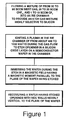
- Figure 1 is a flow sheet illustrating the invention.
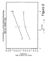
- Figure 2 is a graph depicting the oxide etch rate versus CHF3 concentration plotted as a percentage of the total amount of inept gas and CHF3 flowing into the etching chamber.
- Figure 3 is a graph depicting the contact angle of the etched opening versus CHF3 concentration plotted as a percentage of the total amount of inert gas and CHF3 flowing into the etching chamber.
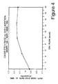
- Figure 4 is a graph depicting the oxide etch rate versus the amount of CF4 flowing into the etching chamber.
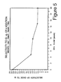
- Figure 5 is a graph depicting the selectivity of the etch to silicon plotted against the amount of CF4 flowing into the etching chamber.
- Figure 6 is a graph depicting the oxide etch rate versus the strength of the magnetic field in the etching chamber.
- the invention comprises an improved process for the plasma etching of an oxide layer on a semiconductor wafer using a combination of an inert gas and CHF3 to provide an oxide etch process highly selective to silicon and which provides a nearly vertical etch slope or contact angle.
- the provision of small amounts of CF4 in the gas flow permits control of the selectivity of the etch process to silicon.
- highly selective to silicon is meant an oxide etch in which the etch ratio of oxide to silicon is at least 15 to 1, up to as high as 27 to 1, depending upon the amount of CF4 present as will be described below.
- nearly vertical etch slope or “nearly vertical contact angle” is meant an angle defined by the sidewall of the opening being formed of at least 80°, preferably about 90°, with the plane of the oxide layer being etched.
- the process of the invention is defined herein as a process for etching silicon dioxide (SiO2)
- SiO2 silicon dioxide
- oxide or glass
- the silicon dioxide etched by the process need not be pure SiO2, but may include other compounds therein, such as, for example, boron, phosphorus, or arsenic compounds, added to lower the melting or flow point of the glass or to impart other desired properties to the glass.
- the etching apparatus used in carrying out the process of the invention may comprise any commercially available reactive ion etching (RIE) apparatus, or magnetically enhanced reactive ion etching (MERIE) apparatus, capable of supporting a wafer of the size desired to be etched in which gases of the type used herein may be introduced at the flow rates to be discussed and a plasma maintained at the power levels required for the process.
- RIE apparatus reactive ion etching
- MIE magnetically enhanced reactive ion etching
- Such apparatus will be generally referred to herein as RIE apparatus, whether magnetically enhanced or not.
- Examples of such commercially available apparatus include the Precision 5000 magnetically enhanced reactive ion etcher available from Applied Materials, Inc.; the Rainbow reactive ion etcher by Lam; the reactive ion apparatus by Tegal Company; and the Quad reactive ion etcher by Drytek.
- the amount of CHF3 which is flowed through the RIE chamber during the etch varies within a range of from about 15 standard cubic centimeters/minute (sccm) to about 60 sccm, depending upon the size of the wafer and the desired etch rate.
- the graph of Figure 2 shows the relationship between the flow of CHF3 (expressed as a volume percentage of total CHF3/inert gas flow versus the etch rate in Angstroms per minute for both a deposited boron phosphorus silicate glass (BPSG) and a thermally grown silicon dioxide (Tox) glass.
- BPSG deposited boron phosphorus silicate glass
- Tox thermally grown silicon dioxide
- the ratio of the flow of inert gas to CHF3 should be maintained within a range of from about 1:1 to about 10:1 to achieve an etch slope or contact angle of at least about 80°.
- the ratio of inert gas flow to flow of CHF3 will vary from at least 2:1 to about 5:1 to achieve an etch slope or contact angle of at least about 85°.
- the contact angle or slope of the etch will vary with CHF3 concentration (shown in Figure 3 as a volume percentage of the total inert gas/CHF3 gas flow) with the highest angles being achieved when the CHF3 concentration ranges from about 20 to 30 volume percent of the total inert gas/CHF3 gas flow, i.e., a ratio range of inert gas to CHF3 of from about 3.33:1 to about 5:1, with a higher angle achieved for a boron phosphorus silicate thermal oxide glass (BPSG) than for a (Tox) glass at the same concentration.
- BPSG boron phosphorus silicate thermal oxide glass
- the pressure is maintained in the RIE chamber within a range of from about 10 milliTorr to about 120 milliTorr, preferably from about 40 milliTorr to about 80 milliTorr.
- the total flow of gases into the RIE chamber should not exceed about 200 sccm. Therefore, the total amount of inert gas which is flowed into the RIE chamber at the same time as the CHF3 will vary within a range of from about 15 sccm to about 185 sccm, and preferably from about 30 sccm to about 140 sccm.
- the inert gas comprises argon, but helium may also be used. However, in the instance of a layer of silicon dioxide over aluminum, the use of helium may be preferred, since argon may sputter the aluminum.
- CF4 may also be flowed into the RIE chamber during the etch.
- the amount of CF4 flowed into the chamber will range from about 2 to about 6 sccm, and most preferably from about 2 to 5 sccm.
- the graph of Figure 4 plots the oxide etch rate against the flow of CF4, while the graph of Figure 5 plots silicon selectivity versus CF4 flow. It will be seen that the addition of CF4 gas to the process increases the oxide etch rate while the selectivity to silicon is reduced as the amount of CF4 in the gas flow is increased.
- the use of CF 4 in the gas flow in accordance with the invention permits control of the amount of selectivity to silicon to provide more precise balancing of the oxide etch rate against silicon selectivity of the etch process.
- the cathode on which the semiconductor wafer is mounted in the RIE chamber during the etch process is cooled down to, and maintained at, a temperature within a range of from about 15°C to about 25° C, preferably about 20°C, to prevent heating of the wafer by the heat generated during the RIE process of the invention.
- the walls of the RIE chamber and the showerhead through which the gases flow into the chamber are heated to a temperature within a range of from about 40°C to about 50°C, for example, by flowing hot water through heat exchangers provided in the walls and showerhead.
- the lid and other top surfaces of the RIE chamber are heated to a temperature within a range of from about 60°C to about 90°C to inhibit depositions on the top of the chamber which might then fall on the wafer. Resistive heaters are usually used to achieve this heating.
- a plasma is ignited between the cathode on which the semiconductor wafer rests and the walls of the chamber using a power source which may be operated at a frequency of about 13.56 megahertz (MHz) and within a power range of from about 400 to about 1000 watts, depending upon the size of the wafer.
- a power source which may be operated at a frequency of about 13.56 megahertz (MHz) and within a power range of from about 400 to about 1000 watts, depending upon the size of the wafer.
- the power level should be within a range of from about 400 to about 500 watts; for a 5" wafer, from about 600 to about 700 watts; for a 6" wafer, from about 650 to about 750 watts; and for an 8" wafer, from about 750 to about 1000 watts.
- the RIE process of the invention is preferably operated in a magnetic field having a magnetic moment or direction of field strength lying in, or parallel to, the plane of the semiconductor wafer.
- the field strength of this magnetic field may range from 1 to about 120 gauss.
- the graph of Figure 6 shows the oxide etch rate plotted against magnetic field strength.
- Such a magnetic field may be provided by permanent magnets or by electromagnetic coils.
- magnetic field generating means such as electromagnetic coils, are disposed around the RIE chamber and then suitably rotated or energized and deenergized to provide a magnetic field of rotating field strength with the magnetic axis rotating parallel to the plane of the wafer.
- Such a magnetic field enhanced RIE apparatus is described and claimed in U.S. Patent 4,842,683, issued June 27, 1989, and assigned to the assignee of this invention, cross-reference to which is hereby made.
- the RIE etch process of the invention may be more efficiently monitored for an end point by emission detection of a CO line, i.e. a 483 nm line, than prior art processes using oxygen gas in the etch gas flow, since the only source of oxygen in the process of the invention is in the oxide being etched, and thus the absence of such a CO line indicates that no further oxide is being etch, i.e., the end point has been reached.
- a CO line i.e. a 483 nm line
- the CHF3/inert gas system of the invention appears to be superior to an Ar/CHF3/O2 RIE process such as practiced in the prior art in providing an anisotropic etch of high selectivity to silicon.
- Plasma polymerization plays an important role when etching SiO2 selectively to silicon. By forming selectively on the sidewalls of etch features, the polymer inhibits isotropic etching.
- results from a Ar/CHF3/O2 prior art process exhibit a thick polymer sidewall and tapered profiles, while results from the process of the invention exhibit a thin polymer sidewall and more vertical profiles.
- the process of the invention seems to decrease the rate of polymerization, it has increased the selective etching of thermal oxide in preference to silicon. During the etch, the horizontal surface remains free of polymer apparently due to a higher ion flux. However, the moment at which the silicon substrate is reached, a thin polymer film begins to form which inhibits further etching and thus enhances selectivity.
- the F/C ratio is the ratio of active species involved in etching SiO2. Increasing the F/C ratio will in-crease the etch rate. Decreasing the ratio enhances polymer formation.
- O2 to the inert gas/CHF3 gas mixture would effectively increases the F/C ratio since carbon is consumed in the formation of CO and CO2.
- the fluorine is consumed at a lower rate in the formation of COF2.
- the process of the invention the major source of oxygen is from the oxide being etched, thus the selectivity to silicon is enhanced due to the lower F/C ratio at the SiO2/Si interface.
- the addition of CF4 to the process provides further control and adjustment of the F/C ratio.
- two 5" diameter silicon wafers respectively having a 1 micron layer of thermally grown oxide (Tox) grown thereon, or a 1 micron layer of boron phosphorus silicate glass (BPSG) deposited thereon, with a photoresist pattern on each wafer having 0.8 micron diameter openings formed therein, were RIE etched in accordance with the process of the invention.
- Tox thermally grown oxide
- BPSG boron phosphorus silicate glass
- Each wafer was placed in the RIE chamber of an Applied Materials 5000 Series magnetically enhanced reactive ion etching system and 60 sccm of argon, 30 sccm of CHF3, and 4 sccm of CF4 was flowed into the chamber, while a vacuum of 80 milliTorr was maintained in the chamber.
- a plasma was ignited using a power level of 650 watts.
- the RIE etch was carried out while monitoring the 483 nm CO emission line.
- a magnetic field parallel to the plane of the wafer of 65 gauss was maintained during each etch.
- the etch rate for the Tox-coated wafer was 3500 Angstroms/minute, while the etch rate for the BPSG-coated wafer was 4300 Angstroms/minute.
- the cross-section of each of the etched wafers was examined using scanning electron microscopy (SEM) to determine the contact angle or slope of the openings as well as the extent of etching of the underlying silicon substrate.
- SEM scanning electron microscopy
- the invention provides an improved silicon oxide etch process comprising an inert gas/CHF3/CF4 mixture in the absence of oxygen characterized by a nearly vertical contact angle and highly selective to silicon with the amount of selectivity controlled by the CF4 to maintain a good oxide etch rate.
Landscapes
- Chemical & Material Sciences (AREA)
- Life Sciences & Earth Sciences (AREA)
- Engineering & Computer Science (AREA)
- Chemical Kinetics & Catalysis (AREA)
- General Chemical & Material Sciences (AREA)
- Geochemistry & Mineralogy (AREA)
- Materials Engineering (AREA)
- Organic Chemistry (AREA)
- Drying Of Semiconductors (AREA)
- ing And Chemical Polishing (AREA)
- Internal Circuitry In Semiconductor Integrated Circuit Devices (AREA)
Applications Claiming Priority (2)
| Application Number | Priority Date | Filing Date | Title |
|---|---|---|---|
| US481135 | 1983-04-01 | ||
| US07/481,135 US5021121A (en) | 1990-02-16 | 1990-02-16 | Process for RIE etching silicon dioxide |
Publications (2)
| Publication Number | Publication Date |
|---|---|
| EP0442488A2 true EP0442488A2 (de) | 1991-08-21 |
| EP0442488A3 EP0442488A3 (en) | 1991-10-16 |
Family
ID=23910758
Family Applications (1)
| Application Number | Title | Priority Date | Filing Date |
|---|---|---|---|
| EP19910102068 Withdrawn EP0442488A3 (en) | 1990-02-16 | 1991-02-14 | Improved process for rie etching silicon dioxide |
Country Status (4)
| Country | Link |
|---|---|
| US (1) | US5021121A (de) |
| EP (1) | EP0442488A3 (de) |
| JP (1) | JP2519839B2 (de) |
| KR (1) | KR910016055A (de) |
Cited By (5)
| Publication number | Priority date | Publication date | Assignee | Title |
|---|---|---|---|---|
| EP0614096A1 (de) * | 1993-03-01 | 1994-09-07 | AT&T Corp. | Verfahren zur Herstellung von Mikrolinsenmatrixen |
| EP0536968A3 (en) * | 1991-10-08 | 1994-12-14 | Nippon Electric Co | Process for forming contact holes in the fabrication of semi-conducteur devices |
| EP0871213A3 (de) * | 1997-03-27 | 1999-03-03 | Siemens Aktiengesellschaft | Verfahren zur Bildung von Kontaktbohrungen mit variablem Seitenwandprofil |
| NL1008180C2 (nl) * | 1997-01-31 | 2002-01-03 | Sony Corp | Werkwijze voor het fabriceren van een halfgeleider inrichting. |
| EP1647535A1 (de) * | 2004-10-09 | 2006-04-19 | Schott AG | Verfahren zur Mikrostrukturierung von Substraten aus Flachglas |
Families Citing this family (51)
| Publication number | Priority date | Publication date | Assignee | Title |
|---|---|---|---|---|
| US5213659A (en) * | 1990-06-20 | 1993-05-25 | Micron Technology, Inc. | Combination usage of noble gases for dry etching semiconductor wafers |
| US5022958A (en) * | 1990-06-27 | 1991-06-11 | At&T Bell Laboratories | Method of etching for integrated circuits with planarized dielectric |
| US5160407A (en) * | 1991-01-02 | 1992-11-03 | Applied Materials, Inc. | Low pressure anisotropic etch process for tantalum silicide or titanium silicide layer formed over polysilicon layer deposited on silicon oxide layer on semiconductor wafer |
| US5176790A (en) * | 1991-09-25 | 1993-01-05 | Applied Materials, Inc. | Process for forming a via in an integrated circuit structure by etching through an insulation layer while inhibiting sputtering of underlying metal |
| US5658425A (en) * | 1991-10-16 | 1997-08-19 | Lam Research Corporation | Method of etching contact openings with reduced removal rate of underlying electrically conductive titanium silicide layer |
| US5242538A (en) * | 1992-01-29 | 1993-09-07 | Applied Materials, Inc. | Reactive ion etch process including hydrogen radicals |
| US5880036A (en) * | 1992-06-15 | 1999-03-09 | Micron Technology, Inc. | Method for enhancing oxide to nitride selectivity through the use of independent heat control |
| US6258497B1 (en) | 1992-07-29 | 2001-07-10 | International Business Machines Corporation | Precise endpoint detection for etching processes |
| US5466636A (en) * | 1992-09-17 | 1995-11-14 | International Business Machines Corporation | Method of forming borderless contacts using a removable mandrel |
| US5468339A (en) * | 1992-10-09 | 1995-11-21 | Advanced Micro Devices, Inc. | Plasma etch process |
| US5468340A (en) * | 1992-10-09 | 1995-11-21 | Gupta; Subhash | Highly selective high aspect ratio oxide etch method and products made by the process |
| US5431799A (en) * | 1993-10-29 | 1995-07-11 | Applied Materials, Inc. | Collimation hardware with RF bias rings to enhance sputter and/or substrate cavity ion generation efficiency |
| JP2993339B2 (ja) * | 1993-12-03 | 1999-12-20 | ヤマハ株式会社 | 半導体装置の製造方法 |
| US6040247A (en) * | 1995-01-10 | 2000-03-21 | Lg Semicon Co., Ltd. | Method for etching contact |
| US6039851A (en) * | 1995-03-22 | 2000-03-21 | Micron Technology, Inc. | Reactive sputter faceting of silicon dioxide to enhance gap fill of spaces between metal lines |
| JP2956524B2 (ja) * | 1995-04-24 | 1999-10-04 | 日本電気株式会社 | エッチング方法 |
| US5814186A (en) * | 1995-08-28 | 1998-09-29 | Advanced Micro Devices, Inc. | SOG etchant gas and method for using same |
| US5631197A (en) * | 1995-08-30 | 1997-05-20 | Taiwan Semiconductor Manufacturing Company, Ltd | Sacrificial etchback layer for improved spin-on-glass planarization |
| US5626716A (en) * | 1995-09-29 | 1997-05-06 | Lam Research Corporation | Plasma etching of semiconductors |
| US5650040A (en) * | 1995-11-30 | 1997-07-22 | Micron Technology, Inc. | Interfacial etch of silica to improve adherence of noble metals |
| US6001699A (en) * | 1996-01-23 | 1999-12-14 | Intel Corporation | Highly selective etch process for submicron contacts |
| US5814563A (en) * | 1996-04-29 | 1998-09-29 | Applied Materials, Inc. | Method for etching dielectric using fluorohydrocarbon gas, NH3 -generating gas, and carbon-oxygen gas |
| US5843847A (en) * | 1996-04-29 | 1998-12-01 | Applied Materials, Inc. | Method for etching dielectric layers with high selectivity and low microloading |
| US5863376A (en) * | 1996-06-05 | 1999-01-26 | Lam Research Corporation | Temperature controlling method and apparatus for a plasma processing chamber |
| TW343360B (en) * | 1996-07-31 | 1998-10-21 | Applied Materials Inc | Plasma reactor process for high photoresist selectivity and improved polymer adhesion |
| US5924000A (en) * | 1997-09-19 | 1999-07-13 | Vanguard International Semiconductor Corporation | Method for forming residue free patterned polysilicon layer containing integrated circuit structures |
| US6074957A (en) * | 1998-02-26 | 2000-06-13 | Micron Technology, Inc. | Methods of forming openings and methods of controlling the degree of taper of openings |
| US6117786A (en) * | 1998-05-05 | 2000-09-12 | Lam Research Corporation | Method for etching silicon dioxide using fluorocarbon gas chemistry |
| US6020268A (en) * | 1998-07-13 | 2000-02-01 | Taiwan Semiconductor Manufacturing Company, Ltd. | Magnetic field controlled spacer width |
| US6117788A (en) * | 1998-09-01 | 2000-09-12 | Micron Technology, Inc. | Semiconductor etching methods |
| US6080676A (en) * | 1998-09-17 | 2000-06-27 | Advanced Micro Devices, Inc. | Device and method for etching spacers formed upon an integrated circuit gate conductor |
| US6136712A (en) * | 1998-09-30 | 2000-10-24 | Lam Research Corporation | Method and apparatus for improving accuracy of plasma etching process |
| US6297163B1 (en) | 1998-09-30 | 2001-10-02 | Lam Research Corporation | Method of plasma etching dielectric materials |
| US6281132B1 (en) | 1998-10-06 | 2001-08-28 | Advanced Micro Devices, Inc. | Device and method for etching nitride spacers formed upon an integrated circuit gate conductor |
| US6335292B1 (en) | 1999-04-15 | 2002-01-01 | Micron Technology, Inc. | Method of controlling striations and CD loss in contact oxide etch |
| US6093079A (en) * | 1999-07-27 | 2000-07-25 | House; William P. | Toy vehicle track |
| US6617257B2 (en) | 2001-03-30 | 2003-09-09 | Lam Research Corporation | Method of plasma etching organic antireflective coating |
| US6630407B2 (en) | 2001-03-30 | 2003-10-07 | Lam Research Corporation | Plasma etching of organic antireflective coating |
| US7311852B2 (en) * | 2001-03-30 | 2007-12-25 | Lam Research Corporation | Method of plasma etching low-k dielectric materials |
| US6864041B2 (en) * | 2001-05-02 | 2005-03-08 | International Business Machines Corporation | Gate linewidth tailoring and critical dimension control for sub-100 nm devices using plasma etching |
| US6746961B2 (en) | 2001-06-19 | 2004-06-08 | Lam Research Corporation | Plasma etching of dielectric layer with etch profile control |
| JP4304904B2 (ja) * | 2002-02-07 | 2009-07-29 | 株式会社島津製作所 | エタロンの製造方法 |
| US7045466B2 (en) * | 2002-06-27 | 2006-05-16 | Cornell Research Foundation, Inc. | Three dimensional high aspect ratio micromachining |
| JP2004246994A (ja) * | 2003-02-14 | 2004-09-02 | Fuji Electric Holdings Co Ltd | マスタディスクの製造方法 |
| KR20050070837A (ko) * | 2003-12-31 | 2005-07-07 | 동부아남반도체 주식회사 | 금속 옥사이드 반도체 소자의 플라즈마 손상방지를 위한식각방법 |
| JP4701776B2 (ja) * | 2005-03-25 | 2011-06-15 | 東京エレクトロン株式会社 | エッチング方法及びエッチング装置 |
| US7517804B2 (en) * | 2006-08-31 | 2009-04-14 | Micron Technologies, Inc. | Selective etch chemistries for forming high aspect ratio features and associated structures |
| US8372756B2 (en) | 2008-08-29 | 2013-02-12 | Air Products And Chemicals, Inc. | Selective etching of silicon dioxide compositions |
| US8445296B2 (en) * | 2011-07-22 | 2013-05-21 | Taiwan Semiconductor Manufacturing Company, Ltd. | Apparatus and methods for end point determination in reactive ion etching |
| KR102799403B1 (ko) * | 2018-02-05 | 2025-04-22 | 램 리써치 코포레이션 | 비정질 탄소 층 개방 프로세스 |
| WO2025032524A1 (en) * | 2023-08-07 | 2025-02-13 | Universidade Do Minho | Thermoelectric micro column array device, methods and uses thereof |
Family Cites Families (18)
| Publication number | Priority date | Publication date | Assignee | Title |
|---|---|---|---|---|
| JPS57159026A (en) * | 1981-03-27 | 1982-10-01 | Toshiba Corp | Dry etching method |
| JPS58143528A (ja) * | 1982-02-22 | 1983-08-26 | Hitachi Ltd | ドライエツチング法 |
| JPS6043844A (ja) * | 1983-08-22 | 1985-03-08 | Toshiba Corp | 半導体装置の製造方法 |
| US4511430A (en) * | 1984-01-30 | 1985-04-16 | International Business Machines Corporation | Control of etch rate ratio of SiO2 /photoresist for quartz planarization etch back process |
| JPS61121440A (ja) * | 1984-11-19 | 1986-06-09 | Matsushita Electric Ind Co Ltd | ドライエツチング方法 |
| US4711698A (en) * | 1985-07-15 | 1987-12-08 | Texas Instruments Incorporated | Silicon oxide thin film etching process |
| JPS6273724A (ja) * | 1985-09-27 | 1987-04-04 | Hitachi Ltd | 半導体装置の製造法 |
| US4668338A (en) * | 1985-12-30 | 1987-05-26 | Applied Materials, Inc. | Magnetron-enhanced plasma etching process |
| US4680087A (en) * | 1986-01-17 | 1987-07-14 | Allied Corporation | Etching of dielectric layers with electrons in the presence of sulfur hexafluoride |
| US4698128A (en) * | 1986-11-17 | 1987-10-06 | Motorola, Inc. | Sloped contact etch process |
| US4842683A (en) * | 1986-12-19 | 1989-06-27 | Applied Materials, Inc. | Magnetic field-enhanced plasma etch reactor |
| EP0282820A1 (de) * | 1987-03-13 | 1988-09-21 | Siemens Aktiengesellschaft | Verfahren zum Erzeugen von Kontaktlöchern mit abgeschrägten Flanken in Zwischenoxidschichten |
| FR2619578A1 (fr) * | 1987-08-18 | 1989-02-24 | Air Liquide | Procede de gravure ionique reactive a basse tension d'autopolarisation par addition de gaz inertes |
| JP2603989B2 (ja) * | 1988-03-18 | 1997-04-23 | 株式会社日立製作所 | 半導体装置の製造方法 |
| US4836885A (en) * | 1988-05-03 | 1989-06-06 | International Business Machines Corporation | Planarization process for wide trench isolation |
| US4904341A (en) * | 1988-08-22 | 1990-02-27 | Westinghouse Electric Corp. | Selective silicon dioxide etchant for superconductor integrated circuits |
| DE69024719T2 (de) * | 1989-08-14 | 1996-10-02 | Applied Materials Inc | Gasverteilungssystem und Verfahren zur Benutzung dieses Systems |
| JPH03101227A (ja) * | 1989-09-14 | 1991-04-26 | Sumitomo Metal Ind Ltd | エッチング方法及びその装置 |
-
1990
- 1990-02-16 US US07/481,135 patent/US5021121A/en not_active Expired - Fee Related
-
1991
- 1991-02-13 KR KR1019910002417A patent/KR910016055A/ko not_active Withdrawn
- 1991-02-14 EP EP19910102068 patent/EP0442488A3/en not_active Withdrawn
- 1991-02-15 JP JP3021246A patent/JP2519839B2/ja not_active Expired - Lifetime
Cited By (6)
| Publication number | Priority date | Publication date | Assignee | Title |
|---|---|---|---|---|
| EP0536968A3 (en) * | 1991-10-08 | 1994-12-14 | Nippon Electric Co | Process for forming contact holes in the fabrication of semi-conducteur devices |
| EP0614096A1 (de) * | 1993-03-01 | 1994-09-07 | AT&T Corp. | Verfahren zur Herstellung von Mikrolinsenmatrixen |
| NL1008180C2 (nl) * | 1997-01-31 | 2002-01-03 | Sony Corp | Werkwijze voor het fabriceren van een halfgeleider inrichting. |
| EP0871213A3 (de) * | 1997-03-27 | 1999-03-03 | Siemens Aktiengesellschaft | Verfahren zur Bildung von Kontaktbohrungen mit variablem Seitenwandprofil |
| EP1647535A1 (de) * | 2004-10-09 | 2006-04-19 | Schott AG | Verfahren zur Mikrostrukturierung von Substraten aus Flachglas |
| US7476623B2 (en) | 2004-10-09 | 2009-01-13 | Schott Ag | Method for microstructuring flat glass substrates |
Also Published As
| Publication number | Publication date |
|---|---|
| JP2519839B2 (ja) | 1996-07-31 |
| US5021121A (en) | 1991-06-04 |
| JPH056875A (ja) | 1993-01-14 |
| KR910016055A (ko) | 1991-09-30 |
| EP0442488A3 (en) | 1991-10-16 |
Similar Documents
| Publication | Publication Date | Title |
|---|---|---|
| US5021121A (en) | Process for RIE etching silicon dioxide | |
| US5880036A (en) | Method for enhancing oxide to nitride selectivity through the use of independent heat control | |
| US5354417A (en) | Etching MoSi2 using SF6, HBr and O2 | |
| JP4657458B2 (ja) | 低容量の誘電体層をエッチングするための技術 | |
| US5814563A (en) | Method for etching dielectric using fluorohydrocarbon gas, NH3 -generating gas, and carbon-oxygen gas | |
| US5286344A (en) | Process for selectively etching a layer of silicon dioxide on an underlying stop layer of silicon nitride | |
| US5431772A (en) | Selective silicon nitride plasma etching process | |
| US6123862A (en) | Method of forming high aspect ratio apertures | |
| US5935874A (en) | Techniques for forming trenches in a silicon layer of a substrate in a high density plasma processing system | |
| JPH10144654A (ja) | 半導体基盤の表面処理方法 | |
| US6297163B1 (en) | Method of plasma etching dielectric materials | |
| US4948462A (en) | Tungsten etch process with high selectivity to photoresist | |
| JPH0740569B2 (ja) | Ecrプラズマ堆積方法 | |
| JPH1041274A (ja) | 誘電層のエッチング方法 | |
| WO2002080234A2 (en) | Method of plasma etching organic antireflective coating | |
| US5362361A (en) | Dry etching method | |
| JPH10125662A (ja) | エッチングプロセス中に側壁プロファイルを制御するための方法および装置 | |
| US6228774B1 (en) | High aspect ratio sub-micron contact etch process in an inductively-coupled plasma processing system | |
| Lee et al. | Effects of magnetic field on oxide etching characteristics in planar type radio frequency inductively coupled plasma | |
| Akimoto et al. | Reactive ion etching lag on high rate oxide etching using high density plasma | |
| US20080203056A1 (en) | Methods for etching high aspect ratio features | |
| Labelle et al. | Metal stack etching using a helical resonator plasma | |
| JPH05304116A (ja) | ドライエッチング装置 | |
| Cho et al. | Improved etch characteristics of SiO 2 by the enhanced inductively coupled plasma | |
| JPH08144072A (ja) | ドライエッチング装置 |
Legal Events
| Date | Code | Title | Description |
|---|---|---|---|
| PUAI | Public reference made under article 153(3) epc to a published international application that has entered the european phase |
Free format text: ORIGINAL CODE: 0009012 |
|
| AK | Designated contracting states |
Kind code of ref document: A2 Designated state(s): DE ES FR GB IT NL |
|
| PUAL | Search report despatched |
Free format text: ORIGINAL CODE: 0009013 |
|
| AK | Designated contracting states |
Kind code of ref document: A3 Designated state(s): DE ES FR GB IT NL |
|
| 17P | Request for examination filed |
Effective date: 19920415 |
|
| 17Q | First examination report despatched |
Effective date: 19920529 |
|
| STAA | Information on the status of an ep patent application or granted ep patent |
Free format text: STATUS: THE APPLICATION HAS BEEN WITHDRAWN |
|
| 18W | Application withdrawn |
Withdrawal date: 19930903 |