EP0442574B1 - Dispositif pour balayer une radiographie - Google Patents
Dispositif pour balayer une radiographie Download PDFInfo
- Publication number
- EP0442574B1 EP0442574B1 EP91200284A EP91200284A EP0442574B1 EP 0442574 B1 EP0442574 B1 EP 0442574B1 EP 91200284 A EP91200284 A EP 91200284A EP 91200284 A EP91200284 A EP 91200284A EP 0442574 B1 EP0442574 B1 EP 0442574B1
- Authority
- EP
- European Patent Office
- Prior art keywords
- electrometer
- photoconductor
- distance
- probes
- signals
- Prior art date
- Legal status (The legal status is an assumption and is not a legal conclusion. Google has not performed a legal analysis and makes no representation as to the accuracy of the status listed.)
- Expired - Lifetime
Links
- 239000000523 sample Substances 0.000 claims description 100
- 239000000758 substrate Substances 0.000 claims description 12
- 230000005855 radiation Effects 0.000 claims description 9
- 230000005520 electrodynamics Effects 0.000 claims description 3
- 238000005259 measurement Methods 0.000 description 34
- 239000000203 mixture Substances 0.000 description 2
- BUGBHKTXTAQXES-UHFFFAOYSA-N Selenium Chemical compound [Se] BUGBHKTXTAQXES-UHFFFAOYSA-N 0.000 description 1
- 239000003990 capacitor Substances 0.000 description 1
- 238000005352 clarification Methods 0.000 description 1
- 238000010276 construction Methods 0.000 description 1
- 230000001419 dependent effect Effects 0.000 description 1
- 238000010586 diagram Methods 0.000 description 1
- 230000000694 effects Effects 0.000 description 1
- 238000001914 filtration Methods 0.000 description 1
- 230000003993 interaction Effects 0.000 description 1
- 229910052711 selenium Inorganic materials 0.000 description 1
- 239000011669 selenium Substances 0.000 description 1
- 230000035945 sensitivity Effects 0.000 description 1
Images

Classifications
-
- G—PHYSICS
- G03—PHOTOGRAPHY; CINEMATOGRAPHY; ANALOGOUS TECHNIQUES USING WAVES OTHER THAN OPTICAL WAVES; ELECTROGRAPHY; HOLOGRAPHY
- G03G—ELECTROGRAPHY; ELECTROPHOTOGRAPHY; MAGNETOGRAPHY
- G03G15/00—Apparatus for electrographic processes using a charge pattern
- G03G15/054—Apparatus for electrographic processes using a charge pattern using X-rays, e.g. electroradiography
-
- G—PHYSICS
- G01—MEASURING; TESTING
- G01T—MEASUREMENT OF NUCLEAR OR X-RADIATION
- G01T1/00—Measuring X-radiation, gamma radiation, corpuscular radiation, or cosmic radiation
- G01T1/29—Measurement performed on radiation beams, e.g. position or section of the beam; Measurement of spatial distribution of radiation
- G01T1/2914—Measurement of spatial distribution of radiation
- G01T1/2921—Static instruments for imaging the distribution of radioactivity in one or two dimensions; Radio-isotope cameras
Definitions
- the invention relates to an arrangement for scanning an X-ray, which is discharged on a previously locally evenly charged photoconductor provided on an electrically conductive substrate depending on the local radiation intensity by means of a plurality of electrometer probes which scan the charge pattern of the photoconductor, a measurement of the distance between the electrometer probes and the photoconductor by means of an alternating voltage coupled to the substrate, which is sensed by means of electrometer probes and filtered out to obtain distance measurement signals.
- the problem here is that the size of the measured charge depends on the distance between the electrometer probes and the photoconductor. To measure this distance, it is provided in the arrangement known from the above-mentioned publication that two outer electrometer probes of the electrometer probe series are not used to determine image values, but rather to to measure the strength of an AC voltage signal coupled to the photoconductor or the substrate. Since this measured signal also depends on the size of the air gap between the electrometer probes and the photoconductor, it can be used to determine the distance. The two electrometer probes for determining the distance are not used for determining image values and, conversely, the electrometer probes for determining the image values are not used for determining the distance.
- the distance values measured by means of the two electrometer probes are now used to computationally determine the actual air gap for each of the electrometer probes and to correct their image signals accordingly.
- the problem here is that for the image electrometer probes lying between the two measuring electrometer probes, their distances can only be approximated by a linear interpolation.
- the photoconductor is usually not planar, so that the distances between at least individual electrometer probes and the photoconductor cannot be correctly determined and, as a result, their image values cannot be optimally corrected.
- the output signals of all electrometer probes are used to determine the image values of the X-ray image
- the output signals of at least some of the electrometer probes are also used to determine the distance measurement signals by means of a suitable filter and that adjustment means are provided by means of the as a function of the measurement signals during the scanning of the X-ray recording continuously the distance between the electrometer probes and the photoconductor is set to a setpoint.
- the output signals of all electrometer probes are used to determine the image values of the X-ray image. It is not necessary to provide electrometer probes which are only used to determine the distance but which do not provide any image values.
- the output signals of at least some of the electrometer probes that are used to determine the image values are used at the same time to determine the distance measurement signals.
- the AC voltage is filtered out, for example, by means of a bandpass filter, which supplies a measurement signal which is dependent on the distance between the photoconductor, which is supplied with the AC voltage via the substrate, and the respective electrometer probe. So that the image signals supplied by the electrometer probes are not disturbed, the frequency of this alternating voltage signal is to be provided such that it lies above the highest frequency occurring in the image signal.
- a low-pass filter must be applied to the image signals so that the AC measurement voltage is filtered out.
- the distance measurement signals filtered out in this way allow direct conclusions to be drawn about the distance.
- Adjustment means are provided by means of which the distance between the electrometer probes and the photoconductor can be adjusted. These adjustment means are now used to determine this distance as a function of the measurement signals during the scanning of an X-ray image continuously readjust so that a specified setpoint is maintained. In this way, it is not necessary to subsequently correct the image values supplied by the electrometer probes. Rather, the distance is continuously set immediately during the recording so that it remains the same and adheres to a specific setpoint.
- the arrangement thus offers the advantage that, due to the ongoing correction of the distance values, the target distance can be kept relatively small, so that the probes only scan the area of the photoconductor assigned to them and not its neighboring areas. This results in a good spatial resolution of the scanned x-ray image.
- the sensitivity of the probes i.e. the signal-to-noise ratio of the signals they deliver has also improved.
- a scanning correction can ideally be carried out individually for each electrometer probe.
- the output signals of all sensors are used to determine both the image values and the distance measurement signals, and that the electrometer probe is adjusted to the desired distance using the measurement signal supplied by it.
- a group of adjacent electrometer probes is positioned by means of the adjustment means, using the measurement signals supplied by them, in such a way that the target distance is maintained on average.
- piezo-electric elements or electro-dynamic means are provided as adjustment means.
- Such adjustment means are simple in construction and yet are able to follow the changes in distance occurring during scanning quickly enough.
- the arrangement provides that the distance measurement signals are obtained from the output signals of the electrometer probes by means of bandpass filters, that the measurement signals filtered in this way are fed to a controller which compares the measurement signals with a setpoint value and controls the adjustment means in this way, that the target distances are maintained.
- the AC voltage signal coupled to the photoconductor must lie in a frequency range outside the signals that occur when the charge image is scanned. It is advantageous to provide the measurement signal in a frequency range above the frequency range of the image values.
- the output signals supplied by the electrometer probes are each fed to a bandpass filter for determining the distance measurement signals, which filters out the corresponding AC voltage signal.
- the measurement signals filtered out in this way are in turn fed to a controller. In this control, each measurement signal supplied by the electrometer probes is marked with a Setpoint compared. If the measured values deviate from the desired signal, the adjustment means assigned to the corresponding electrometer probe are activated in such a way that the distance measurement signals again assume the desired value.
- the target distance between the respective electrometer probe and the photoconductor is then also set. In this way, during the scanning of a charge image on the photoconductor, in which the photoconductor is moved relative to the row of electrometer probes, the distance between the electrometer probes and the photoconductor is continuously corrected.
- FIG. 1 shows a circuit diagram of an arrangement for scanning an X-ray image with electrometer probes, the output signals of which are used both for determining image values and for determining distance measurement signals.
- the corresponding signal processing is mostly shown only for an electrometer probe. However, appropriate signal processing is actually provided for each electrometer probe.
- FIG. 1 schematically shows a photoconductor 1 which is provided on an electrically conductive substrate 2.
- This photoconductor 1 can either be flat, as indicated in the figure, but it can also have a drum shape.
- the photoconductor is uniformly electrically charged before an X-ray exposure in a manner not shown in the figure.
- the photoconductor is then discharged to different extents depending on the intensity of the x-rays in a manner not shown in the figure. This resulting charge image is then scanned.
- the photoconductor 1 is also connected via the substrate 2 and via a capacitor 4 to an AC voltage source 5, which for example generates an AC voltage signal with a frequency of 16 kHz.
- This AC voltage signal is coupled to the substrate 2 via the capacitance 4 and is used to generate the distance measurement signals.
- an electrometer probe 6 is indicated at a certain distance from the photoconductor 1, which has a centrally arranged scanning electrode 7 and shielding electrodes 8 arranged around the scanning electrode 7. 1, only one electrometer probe 6 is indicated; however, an arrangement for scanning a charge pattern actually contains several such electrometer probes 6.
- the scanning electrode 7 of the electrometer probe 6 is connected to an input 9 of an operational amplifier 10, which amplifies the signals supplied by the electrometer probe 6.
- the output signal of the amplifier 10 is fed back to a further input 11 of the amplifier.
- One of the inputs 9 or 11 of the operational amplifier is the negative input, so that the operational amplifier works as an impedance converter.
- the amplifier 10 has an input capacitance, which is shown in FIG. 1 for clarification as a discrete capacitance 12 connected to ground.
- the scanning electrode 7 of the electrometer probe 6 is also connected to a switch 13, by means of which the scanning electrode can be switched to ground and is used to discharge any charges present before scanning an X-ray image.
- the output signal of the amplifier 10 is fed to a first signal processing unit 14, in which the signals required for the generation of the image values are filtered out.
- a first signal processing unit 14 in which the signals required for the generation of the image values are filtered out.
- an amplifier 15 is provided in the signal processing unit 14.
- the amplifier 15 is followed by a low-pass filter 16, which may have a cut-off frequency of approximately 2 kHz, for example.
- the output signal of the filter 16 is fed to an image processing unit 17, which is a multiplexer 18 has.
- the multiplexer 18 has, as indicated in the figure by means of several arrows, as many inputs as there are electrometer probes for scanning. Each of the inputs is connected to a complete signal processing branch with an electrometer probe 6, amplifier 10 and signal processing unit 14. In this way, the low-pass filtered output signals of all electrometer probes provided in an arrangement reach the multiplexer 18.
- An analog / digital converter 19 is connected downstream of the multiplexer 18 in the image processing unit 17 and converts the image values into digital values.
- a signal processor 20 can then be connected downstream of the analog / digital converter, for example, which is only indicated schematically in the figure and by means of which the image values can be processed further.
- the output signals of the amplifier 10 are also fed to a second signal processing unit 21, in which the distance measurement signals are obtained.
- an amplifier 22 is initially provided in this unit 21, the output signals of which are fed to a bandpass filter 23 which is tuned to the frequency of the AC voltage generator 5.
- the output signals of the bandpass filter 23 are rectified by means of a rectifier 24.
- the signals rectified in this way are fed to a low-pass filter 25 which, for example, has an upper cut-off frequency of approximately 800 Hz.
- a voltage signal is therefore available at the output of the low-pass filter 25, the size of which represents a measure of the distance between the electrometer probe 6 and the photoconductor 1.
- This output signal of the low-pass filter 25 is fed to a control unit 26.
- the control unit 26 has as many inputs as probes are provided. Each of the inputs is connected to an electrometer probe 6 and the subsequent associated signal processing.
- the control unit 26 compares the measurement signals supplied to it with a setpoint value supplied at an input 27 and, as a function of these comparisons, generates an output signal available at outputs 28, which actuates adjustment means (not shown in FIG. 1) by means of which the respective electrometer probes are returned to theirs Target distance to be positioned.
- This signal thus amplified thus contains both the signals which are based on the charge pattern generated by the X-ray radiation and the signals which are based on that of the AC voltage generator 5 supplied AC voltage decrease.
- This signal mixture is now supplied on the one hand to the first signal processing unit 14, in which those signal components which are required for generating the image values are filtered out by means of a low-pass filter.
- the higher-frequency signal components, which go back to the AC voltage generator 5, are suppressed by means of the low-pass filter.
- the low-pass filter 16 there are only the signals based on the charge pattern.
- These signals are then processed further in the image processing unit 17. This takes place in a corresponding manner for all sensors which are provided in an arrangement which is not shown in the figure.
- the signal mixture leaving the amplifier 10 is also fed to the second signal processing unit 21 for generating the distance measurement signals.
- the second signal processing unit 21 for generating the distance measurement signals.
- the signal component which was induced on the electrometer probe 6 as a result of the alternating voltage supplied by the generator 5 is filtered out by means of the bandpass filter 23. Only this measurement signal is processed further by first rectifying it and then low-pass filtering it. A voltage signal is then available which represents the distance measurement signal and whose size represents a measure of the distance between the electrometer probe 6 and the photoconductor 1. This distance measurement signal is then fed to the control unit 26. This applies in a manner not shown in FIG. 1 for all distance measurement signals of the arrangement.
- the distance measurement signals are compared with a target value, which represents a target distance between the electrometer probes and the photoconductor.
- a target value which represents a target distance between the electrometer probes and the photoconductor.
- the Control unit 26 has a signal available at the outputs 27, which controls the control means assigned to the respective electrometer probes in such a way that their distance measurement signals again assume the desired value, that is to say the desired distance between the electrometer probe and the photoconductor is restored.
- U in - Q s / C in
- Q s the influential charge applied to the sensing electrode 7 of the electrometer probe 6.
- C in is the total capacitance at the input of the amplifier 10, which is shown in the illustration in FIG. 1 as an external, separate capacitance 12.
- control unit 26 depending on the comparison of the distance measurement signal of each probe with a setpoint signal, outputs a corresponding control signal to adjusting means, which are the respective associated electrometer probe, or also a group of electrometer probes, in their distance relative to the photoconductor 1 adjust.
- adjusting means which are the respective associated electrometer probe, or also a group of electrometer probes, in their distance relative to the photoconductor 1 adjust.
- adjustment means can be provided individually for each electrometer probe.
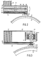
- An electrometer probe and associated adjustment means are shown in section.
- An electrometer probe 6 has a scanning electrode 4 and shielding electrodes 8.
- the scanning electrode 4, on which the charges to be measured are influenced, is provided with an electrical connection 31, which is connected in a manner not shown in FIG. 2 to the input 9 of the amplifier 10 according to FIG. 1, for example.
- the photoconductor 32 shows a photoconductor 32 below the electrometer probe 6, which is provided on a carrier substrate 33.
- the photoconductor 32 has a drum shape in its entirety and is moved relative to the electrometer probe 6 in order to scan the charge pattern stored on it, charges being influenced in the scanning electrode 4 in accordance with the charge pattern.
- adjustment means In order to adjust the distance between the electrometer probe 6 and the surface of the photoconductor 32, adjustment means are provided which have a holder 34 which is fixed in place in a manner not shown in FIG. 2 and two piezoelectric elements 35 and 36.
- the holder 34, the two piezoelectric elements 35 and 36 and the electrometer probe 6 are surrounded by a common, electrically conductive sheath 37 which is electrically grounded.
- the electrometer probe 6 is mechanically connected to the piezoelectric elements 35 and 36 by means of this shield 37.
- An electrode 38 is provided between the two piezoelectric elements 35 and 36, which in turn is connected to an electrical connection 39.
- This electrode 38 serves to supply the two piezoelectric elements 35 and 36 with electrical voltages which, due to the piezoelectric effect of the elements 35 and 36, lead to their deformation.
- the arrangement is designed so that the two piezoelectric elements react in opposite directions. If the piezoelectric element 35 expands with a corresponding signal at the electrode 38, the element 36 contracts. The same applies in reverse. When the piezoelectric element 35 expands while the element 36 contracts, the distance between the electrometer probe 6 and the surface of the photoconductor 32 is reduced. Conversely, when the piezoelectric element 36 expands or the element 35 contracts, the distance is increased.
- an arrangement according to FIG. 2 can have a length of the piezoelectric elements 35 and 36 of approximately 1 cm, which, at control voltages of approximately 10 V, allows the arrangement in the area of the electrometer probe to be deflected by approximately 100 ⁇ m.
- This concept also enables a high control bandwidth, ie the adjustment means are able to follow control signals up to a few 100 Hz. It is therefore possible to compensate for any fluctuations in distance that occur, even at higher scanning speeds, for example a relative speed to the photoconductor of 5 m / s.
- An arrangement shown in section in FIG. 3 also has an electrometer probe 4, which is provided with an external electrical connection 31 and is constructed in the same way as the probe 6 shown in FIG. 2.
- a drum-shaped substrate 32 is provided, which is provided with a photoconductor 33.
- the arrangement according to FIG. 3 has a support block 41 which is connected via an elastic tongue 42 to a core 43, the other side of which is mechanically connected to the outer shield 37 of the electrometer probe 6.
- a support block 41 which is connected via an elastic tongue 42 to a core 43, the other side of which is mechanically connected to the outer shield 37 of the electrometer probe 6.
- two permanent magnet rings 45 and 46 are provided, which are mounted on the core 43 and extend around it.
- a solenoid 44 is also provided which is mechanically connected to the support block 41, i.e. is stationary.
- the electrical signal for the magnetic coil 44 is obtained in a manner corresponding to the control signal for the adjusting means according to FIG. 2.
Landscapes
- General Physics & Mathematics (AREA)
- Health & Medical Sciences (AREA)
- Physics & Mathematics (AREA)
- Molecular Biology (AREA)
- Life Sciences & Earth Sciences (AREA)
- High Energy & Nuclear Physics (AREA)
- Pathology (AREA)
- Spectroscopy & Molecular Physics (AREA)
- Analysing Materials By The Use Of Radiation (AREA)
- Control Or Security For Electrophotography (AREA)
- Transforming Light Signals Into Electric Signals (AREA)
- Radiography Using Non-Light Waves (AREA)
- Electrophotography Using Other Than Carlson'S Method (AREA)
- Apparatus For Radiation Diagnosis (AREA)
- Length-Measuring Devices Using Wave Or Particle Radiation (AREA)
Claims (10)
- Dispositif pour balayer une radiographie, qui est présente sur un photoconducteur (1) préalablement chargé localement de manière uniforme et prévu sur un substrat conducteur de l'électricité (2), lequel photoconducteur est déchargé en fonction de l'intensité du rayonnement local au moyen de plusieurs sondes électrométriques (6), qui balaient le motif de charges du photoconducteur (1), une mesure de la distance entre les sondes électrométriques (6) et le photoconducteur (1) étant effectué au moyen d'une tension alternative appliquée au substrat, qui est balayée au moyen de sondes électrométriques et extraite par filtrage pour obtenir des signaux de mesure de distance, caractérisé en ce que les signaux de sortie de toutes les sondes électrométriques (6) contribuent à la détermination des valeurs d'image de la radiographie, que les signaux de sortie d'au moins certaines des sondes électrométriques (6) contribuent également à la détermination des signaux de mesure de distance au moyen d'un filtre approprié (3) et que des moyens de réglage sont envisagés à l'intervention desquels la distance entre les sondes électrométriques (6) et le photoconducteur (1) sera réglée sur une valeur de consigne en continu en fonction des signaux de mesure au cours du balayage de la radiographie.
- Dispositif selon la revendication 1, caractérisé en ce que les signaux de sortie de toutes les sondes électrométriques (6) contribuent à la détermination à la fois des valeurs d'image et des signaux de mesure de distance.
- Dispositif selon la revendication 2, caractérisé en ce que, via les moyens de réglage, chaque sonde électrométrique (6) est réglée à la distance de consigne en mettant à contribution le signal de mesure fourni par cette sonde.
- Dispositif selon la revendication 2, caractérisé en ce que, via les moyens de réglage, chaque fois un groupe de sondes électrométriques voisines (6) est positionné par mise en oeuvre des signaux de mesure délivrés par ces sondes, de telle sorte que la distance de consigne soit maintenue en moyenne.
- Dispositif selon l'une quelconque des revendications 1 à 4, caractérisé en ce que des moyens de réglage piézo-électriques sont prévus.
- Dispositif selon l'une quelconque des revendications 1 à 4, caractérisé en ce que des moyens de réglage électrodynamiques sont prévus.
- Dispositif selon l'une quelconque des revendications 1 à 6, caractérisé en ce que les signaux de mesure de distance sont obtenus via des filtres passe-bande (23) à partir des signaux de sortie des sondes électrométriques (6), que les signaux de mesure ainsi filtrés sont acheminés à un système de commande (26) qui compare les signaux de mesure à une valeur de consigne et qui commande les moyens de réglage, de telle sorte que les distances de consigne soient respectées.
- Dispositif selon l'une quelconque des revendications 1 à 7, caractérisé en ce que le photoconducteur (1) s'étend dans un plan.
- Dispositif selon l'une quelconque des revendications 1 à 7, caractérisé en ce que le photoconducteur (1) a la forme d'un tambour.
- Appareil d'examen radiographique, caractérisé en ce qu'un dispositif selon l'une quelconque des revendications 1 à 9, est prévu.
Applications Claiming Priority (2)
| Application Number | Priority Date | Filing Date | Title |
|---|---|---|---|
| DE4004348A DE4004348A1 (de) | 1990-02-13 | 1990-02-13 | Anordnung zum abtasten einer roentgenaufnahme |
| DE4004348 | 1990-02-13 |
Publications (2)
| Publication Number | Publication Date |
|---|---|
| EP0442574A1 EP0442574A1 (fr) | 1991-08-21 |
| EP0442574B1 true EP0442574B1 (fr) | 1994-08-10 |
Family
ID=6400017
Family Applications (1)
| Application Number | Title | Priority Date | Filing Date |
|---|---|---|---|
| EP91200284A Expired - Lifetime EP0442574B1 (fr) | 1990-02-13 | 1991-02-11 | Dispositif pour balayer une radiographie |
Country Status (4)
| Country | Link |
|---|---|
| US (1) | US5097493A (fr) |
| EP (1) | EP0442574B1 (fr) |
| JP (1) | JPH05346710A (fr) |
| DE (2) | DE4004348A1 (fr) |
Families Citing this family (12)
| Publication number | Priority date | Publication date | Assignee | Title |
|---|---|---|---|---|
| DE4129469A1 (de) * | 1991-09-05 | 1993-03-11 | Philips Patentverwaltung | Photoleiteranordnung mit einer ausleseeinheit |
| DE4205566A1 (de) * | 1992-02-22 | 1993-08-26 | Philips Patentverwaltung | Verfahren fuer roentgenaufnahmen und dafuer geeignete vorrichtung |
| DE4330366A1 (de) * | 1993-09-08 | 1995-03-09 | Philips Patentverwaltung | Verfahren zum Erzeugen von Röntgenaufnahmen und Anordnung zur Durchführung des Verfahrens |
| DE19511286A1 (de) * | 1995-03-28 | 1996-10-02 | Philips Patentverwaltung | Röntgenaufnahmegerät mit einem Photoleiter und einer Aufladeeinrichtung |
| IL123006A (en) | 1998-01-20 | 2005-12-18 | Edge Medical Devices Ltd | X-ray imaging system |
| IL126018A0 (en) | 1998-09-01 | 1999-05-09 | Edge Medical Devices Ltd | X-ray imaging system |
| US6326625B1 (en) | 1999-01-20 | 2001-12-04 | Edge Medical Devices Ltd. | X-ray imaging system |
| US6178225B1 (en) | 1999-06-04 | 2001-01-23 | Edge Medical Devices Ltd. | System and method for management of X-ray imaging facilities |
| US8923956B2 (en) | 2001-12-07 | 2014-12-30 | The University Of Sussex | Electrodynamic sensors and applications thereof |
| GB0129390D0 (en) * | 2001-12-07 | 2002-01-30 | Clark Terrence D | Electrodynamic sensors and applications thereof |
| US7149600B2 (en) * | 2003-10-08 | 2006-12-12 | Waterfall Inc. | Pipe storage and inventory control chest |
| JP4157455B2 (ja) * | 2003-10-08 | 2008-10-01 | 株式会社東芝 | X線診断装置及び撮像系移動制御方法 |
Family Cites Families (4)
| Publication number | Priority date | Publication date | Assignee | Title |
|---|---|---|---|---|
| US4134137A (en) * | 1976-11-01 | 1979-01-09 | Xerox Corporation | Single wire microelectrometer imaging system |
| JPS6052413B2 (ja) * | 1979-07-11 | 1985-11-19 | 富士写真フイルム株式会社 | 放射線画像情報読取装置 |
| JP2582561B2 (ja) * | 1987-01-27 | 1997-02-19 | 富士写真フイルム 株式会社 | 放射線画像情報読取方法および装置 |
| JPH0721621B2 (ja) * | 1987-04-16 | 1995-03-08 | 富士写真フイルム株式会社 | 放射線画像の分割パタ−ン認識方法 |
-
1990
- 1990-02-13 DE DE4004348A patent/DE4004348A1/de not_active Withdrawn
-
1991
- 1991-02-11 DE DE59102458T patent/DE59102458D1/de not_active Expired - Fee Related
- 1991-02-11 EP EP91200284A patent/EP0442574B1/fr not_active Expired - Lifetime
- 1991-02-12 US US07/655,006 patent/US5097493A/en not_active Expired - Fee Related
- 1991-02-13 JP JP3020062A patent/JPH05346710A/ja active Pending
Also Published As
| Publication number | Publication date |
|---|---|
| JPH05346710A (ja) | 1993-12-27 |
| EP0442574A1 (fr) | 1991-08-21 |
| US5097493A (en) | 1992-03-17 |
| DE59102458D1 (de) | 1994-09-15 |
| DE4004348A1 (de) | 1991-08-14 |
Similar Documents
| Publication | Publication Date | Title |
|---|---|---|
| EP0212733B1 (fr) | Procédé et appareil pour la production d'images à rayons X par photoconducteur | |
| EP0442574B1 (fr) | Dispositif pour balayer une radiographie | |
| DE2813947C2 (de) | Verfahren zur berührungslosen Messung des Potentialverlaufs in einem elektronischen Bauelement und Anordnung zur Durchführung des Verfahrens | |
| DE2814049C2 (fr) | ||
| DE3733776A1 (de) | Ultraschallsonde | |
| EP1110169B1 (fr) | Procede pour l'acquisition capacitive d'images | |
| EP0466956A1 (fr) | Appareil de tomographie | |
| DE10135427A1 (de) | Flächenhafter Bilddetektor für elektromagnetische Strahlen, insbesondere Röntgenstrahlen | |
| DE3882044T2 (de) | Vorrichtung zur schlitzradiographie mit bild-egalisierung. | |
| EP1691217B1 (fr) | Procédé et appareil pour lire des vues radiographiques enregistrées dans un écran luminescent | |
| DE2948660A1 (de) | Influenzsondenanordnung und verfahren zu ihrer herstellung | |
| DE4233830C2 (de) | Strahlpositionsmonitor | |
| EP1691216A1 (fr) | Système radiographique et méthode d'enregistrement des radiographies dans des feuilles photostimulables | |
| DE3783766T2 (de) | Atto-amperemessgeraet. | |
| EP0558116B1 (fr) | Procédé pour radiographies et dispositif approprié | |
| EP0517302B1 (fr) | Installation de production de radiographies | |
| EP0444737B1 (fr) | Dispositif pour la lecture par balayage d'une radiographie | |
| EP0310816B1 (fr) | Poursuite automatique de fréquence dans un procédé mesureur de rayons corpusculaires utilisant un rayon primaire modulé | |
| DE3815458A1 (de) | Anordnung zur erzeugung von roentgenaufnahmen mittels eines photoleiters | |
| EP0642265B1 (fr) | Procédé et appareil pour la génération de radiographies | |
| DE69015624T2 (de) | Verfahren und vorrichtung für röntgenaufnahmen mit schlitzblenden. | |
| EP0570389B1 (fr) | Procede et dispositif pour la mesure sans contact de tensions electriques dans un objet a mesurer comportant une surface isolante | |
| DE102018207418B4 (de) | Referenzspannungssystem für einen Strahlungsdetektor | |
| EP1075014A2 (fr) | Détecteur à chambre à gaz comportant un multiplicateur d'électrons à gaz | |
| EP0948817A1 (fr) | Capteur d'images en couleurs a couplage de charge |
Legal Events
| Date | Code | Title | Description |
|---|---|---|---|
| PUAI | Public reference made under article 153(3) epc to a published international application that has entered the european phase |
Free format text: ORIGINAL CODE: 0009012 |
|
| AK | Designated contracting states |
Kind code of ref document: A1 Designated state(s): DE FR GB |
|
| 17P | Request for examination filed |
Effective date: 19920221 |
|
| 17Q | First examination report despatched |
Effective date: 19931102 |
|
| GRAA | (expected) grant |
Free format text: ORIGINAL CODE: 0009210 |
|
| AK | Designated contracting states |
Kind code of ref document: B1 Designated state(s): DE FR GB |
|
| REF | Corresponds to: |
Ref document number: 59102458 Country of ref document: DE Date of ref document: 19940915 |
|
| GBT | Gb: translation of ep patent filed (gb section 77(6)(a)/1977) |
Effective date: 19941026 |
|
| ET | Fr: translation filed | ||
| REG | Reference to a national code |
Ref country code: FR Ref legal event code: CD |
|
| PLBE | No opposition filed within time limit |
Free format text: ORIGINAL CODE: 0009261 |
|
| STAA | Information on the status of an ep patent application or granted ep patent |
Free format text: STATUS: NO OPPOSITION FILED WITHIN TIME LIMIT |
|
| 26N | No opposition filed | ||
| PGFP | Annual fee paid to national office [announced via postgrant information from national office to epo] |
Ref country code: GB Payment date: 19970203 Year of fee payment: 7 |
|
| PGFP | Annual fee paid to national office [announced via postgrant information from national office to epo] |
Ref country code: FR Payment date: 19970218 Year of fee payment: 7 |
|
| PGFP | Annual fee paid to national office [announced via postgrant information from national office to epo] |
Ref country code: DE Payment date: 19970422 Year of fee payment: 7 |
|
| PG25 | Lapsed in a contracting state [announced via postgrant information from national office to epo] |
Ref country code: GB Free format text: LAPSE BECAUSE OF NON-PAYMENT OF DUE FEES Effective date: 19980211 |
|
| PG25 | Lapsed in a contracting state [announced via postgrant information from national office to epo] |
Ref country code: FR Free format text: THE PATENT HAS BEEN ANNULLED BY A DECISION OF A NATIONAL AUTHORITY Effective date: 19980228 |
|
| GBPC | Gb: european patent ceased through non-payment of renewal fee |
Effective date: 19980211 |
|
| PG25 | Lapsed in a contracting state [announced via postgrant information from national office to epo] |
Ref country code: DE Free format text: LAPSE BECAUSE OF NON-PAYMENT OF DUE FEES Effective date: 19981103 |
|
| REG | Reference to a national code |
Ref country code: FR Ref legal event code: ST |