EP0442792A1 - Lichtwellenleiter-elektrooptische Vorrichtung, insbesondere für Polarisationsteiler - Google Patents
Lichtwellenleiter-elektrooptische Vorrichtung, insbesondere für Polarisationsteiler Download PDFInfo
- Publication number
- EP0442792A1 EP0442792A1 EP91400323A EP91400323A EP0442792A1 EP 0442792 A1 EP0442792 A1 EP 0442792A1 EP 91400323 A EP91400323 A EP 91400323A EP 91400323 A EP91400323 A EP 91400323A EP 0442792 A1 EP0442792 A1 EP 0442792A1
- Authority
- EP
- European Patent Office
- Prior art keywords
- phase shift
- guides
- optical
- electro
- coupler
- Prior art date
- Legal status (The legal status is an assumption and is not a legal conclusion. Google has not performed a legal analysis and makes no representation as to the accuracy of the status listed.)
- Granted
Links
- 230000010363 phase shift Effects 0.000 claims abstract description 52
- 239000000758 substrate Substances 0.000 claims abstract description 34
- 230000003287 optical effect Effects 0.000 claims abstract description 28
- 230000010287 polarization Effects 0.000 claims description 33
- 230000003993 interaction Effects 0.000 claims description 20
- 230000008878 coupling Effects 0.000 claims description 10
- 238000010168 coupling process Methods 0.000 claims description 10
- 238000005859 coupling reaction Methods 0.000 claims description 10
- 230000005684 electric field Effects 0.000 claims description 8
- 230000001902 propagating effect Effects 0.000 claims description 6
- 230000004044 response Effects 0.000 claims description 2
- 235000021183 entrée Nutrition 0.000 description 10
- 230000000694 effects Effects 0.000 description 3
- 239000000463 material Substances 0.000 description 3
- 230000008859 change Effects 0.000 description 2
- 230000001427 coherent effect Effects 0.000 description 2
- 239000011159 matrix material Substances 0.000 description 2
- 239000013307 optical fiber Substances 0.000 description 2
- 230000005693 optoelectronics Effects 0.000 description 2
- 230000009467 reduction Effects 0.000 description 2
- 239000010936 titanium Substances 0.000 description 2
- RTAQQCXQSZGOHL-UHFFFAOYSA-N Titanium Chemical compound [Ti] RTAQQCXQSZGOHL-UHFFFAOYSA-N 0.000 description 1
- 240000008042 Zea mays Species 0.000 description 1
- 230000006978 adaptation Effects 0.000 description 1
- 230000008901 benefit Effects 0.000 description 1
- 239000000470 constituent Substances 0.000 description 1
- 230000007423 decrease Effects 0.000 description 1
- 238000009792 diffusion process Methods 0.000 description 1
- 230000005284 excitation Effects 0.000 description 1
- 238000002347 injection Methods 0.000 description 1
- 239000007924 injection Substances 0.000 description 1
- GQYHUHYESMUTHG-UHFFFAOYSA-N lithium niobate Chemical compound [Li+].[O-][Nb](=O)=O GQYHUHYESMUTHG-UHFFFAOYSA-N 0.000 description 1
- 238000004519 manufacturing process Methods 0.000 description 1
- 238000000926 separation method Methods 0.000 description 1
- 229910052719 titanium Inorganic materials 0.000 description 1
Images


Classifications
-
- G—PHYSICS
- G02—OPTICS
- G02F—OPTICAL DEVICES OR ARRANGEMENTS FOR THE CONTROL OF LIGHT BY MODIFICATION OF THE OPTICAL PROPERTIES OF THE MEDIA OF THE ELEMENTS INVOLVED THEREIN; NON-LINEAR OPTICS; FREQUENCY-CHANGING OF LIGHT; OPTICAL LOGIC ELEMENTS; OPTICAL ANALOGUE/DIGITAL CONVERTERS
- G02F1/00—Devices or arrangements for the control of the intensity, colour, phase, polarisation or direction of light arriving from an independent light source, e.g. switching, gating or modulating; Non-linear optics
- G02F1/29—Devices or arrangements for the control of the intensity, colour, phase, polarisation or direction of light arriving from an independent light source, e.g. switching, gating or modulating; Non-linear optics for the control of the position or the direction of light beams, i.e. deflection
- G02F1/31—Digital deflection, i.e. optical switching
- G02F1/313—Digital deflection, i.e. optical switching in an optical waveguide structure
- G02F1/3136—Digital deflection, i.e. optical switching in an optical waveguide structure of interferometric switch type
-
- G—PHYSICS
- G02—OPTICS
- G02F—OPTICAL DEVICES OR ARRANGEMENTS FOR THE CONTROL OF LIGHT BY MODIFICATION OF THE OPTICAL PROPERTIES OF THE MEDIA OF THE ELEMENTS INVOLVED THEREIN; NON-LINEAR OPTICS; FREQUENCY-CHANGING OF LIGHT; OPTICAL LOGIC ELEMENTS; OPTICAL ANALOGUE/DIGITAL CONVERTERS
- G02F1/00—Devices or arrangements for the control of the intensity, colour, phase, polarisation or direction of light arriving from an independent light source, e.g. switching, gating or modulating; Non-linear optics
- G02F1/01—Devices or arrangements for the control of the intensity, colour, phase, polarisation or direction of light arriving from an independent light source, e.g. switching, gating or modulating; Non-linear optics for the control of the intensity, phase, polarisation or colour
- G02F1/0136—Devices or arrangements for the control of the intensity, colour, phase, polarisation or direction of light arriving from an independent light source, e.g. switching, gating or modulating; Non-linear optics for the control of the intensity, phase, polarisation or colour for the control of polarisation, e.g. state of polarisation [SOP] control, polarisation scrambling, TE-TM mode conversion or separation
- G02F1/0144—TE-TM mode separation
-
- G—PHYSICS
- G02—OPTICS
- G02F—OPTICAL DEVICES OR ARRANGEMENTS FOR THE CONTROL OF LIGHT BY MODIFICATION OF THE OPTICAL PROPERTIES OF THE MEDIA OF THE ELEMENTS INVOLVED THEREIN; NON-LINEAR OPTICS; FREQUENCY-CHANGING OF LIGHT; OPTICAL LOGIC ELEMENTS; OPTICAL ANALOGUE/DIGITAL CONVERTERS
- G02F2202/00—Materials and properties
- G02F2202/20—LiNbO3, LiTaO3
Definitions
- the present invention relates to an electro-optical device with light guides which can be produced in integrated form on a crystalline substrate.
- a device typically has three optical terminals constituting an input and two outputs. A light vibration arriving on this input is directed towards one or the other of these outputs according to its direction of polarization and the values of electric control voltages applied to the guides formed in the substrate.
- the device can thus constitute a polarization splitter for an input light composed of two mutually perpendicular vibrations of linear polarizations:
- the control voltages being kept constant the two vibrations are separated and directed respectively to the two outputs.
- a first known device has been proposed to constitute such a switch. It has been described by T. POHLMANN, A. NEYER, E. VOGES, in the article entitled "Ti: LiNb03 interferometric activated X - switch for high-speed application: IAX" in the journal Electronics Letters, Vol 24, n ° 9, pages 530-531 of April 28, 1988.
- This known device comprises optical guides perpendicular to the crystallographic axis Z which is the single optical axis of the crystalline substrate on which these guides are produced. Its use as a polarization splitter would require the use of high control voltages and very strict manufacturing conditions to obtain an X coupler independent of polarization.
- a second circuit is known to constitute a polarization splitter. It was described by Y.BOURBIN, in the article entitled “Polarization splitter in integrated optics” presented at the "5th European Conference on Integrated Optics ECIO 89", April 24-28, 89 in Paris. It uses an active directional coupler whose optical excitation is symmetrical and where the orthogonal polarizations (TE and TM mode) see equal and opposite index variations due to equal and opposite electro-optical coefficients.
- the use of an active directional coupler requires mutual adaptation of the optical parts and the electrical part: The dimensions of the coupler (length, distance between guides) impose the dimensions of the electrodes (length, distance between electrodes).
- a reduction in control voltages can be obtained, as in other devices, by an increase in the length of the electrodes. But the use of a directional coupler then requires an increase in the distance between the electrodes and this increase in distance is opposed to a reduction in the control voltages. The latter can therefore only be reduced to a small extent following an increase in length. The latter is also done at the expense of the optical bandwidth which decreases when the length increases.
- the object of the present invention is in particular to provide in a simple manner an electro-optical device with light guides which can be used with limited control voltages for various polarization states of an input light wave.
- a device of this kind comprising a pair of guides formed in a crystalline substrate to achieve an electro-optical phase shift of 90 degrees, and followed by a half-power coupler, this device being characterized in that this phase shift is carried out in guides parallel to the single optical axis of this substrate so that two light vibrations of perpendicular polarizations see two electro-optical coefficients of the same absolute value and of opposite algebraic signs.
- FIG. 1 represents a perspective view of the crystalline substrate carrying the optical guides of a first device according to the present invention.
- FIG. 2 represents a perspective view of this first device.
- Figure 3 shows a cross-sectional view of this first device.
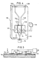
- FIG. 4 represents a perspective view of a second device according to the present invention.
- Figure 5 shows a cross-sectional view of this second device.
- Figure 6 shows a cross-sectional view of a third device according to the present invention.
- Figure 7 shows a cross-sectional view of a fourth device according to the present invention.
- FIGS. 1 to 3 indicate in general terms various arrangements which are preferred according to the present invention, at least in certain applications, and which are adopted in the four devices given as an example. Some of these provisions are common to these devices according to the invention and to the first known device mentioned above, while others are specific to the present invention.
- the coupler thus formed is of the so-called “directional coupler” type. It could however be of another type such as that known as "X coupler”.
- Another said preferred arrangement is specific to the present invention.
- phase shift guides 4A, 4B extend parallel to the single optical axis Z of said crystalline substrate 6, said interaction direction Y being perpendicular to this optical axis and such that the electro-optical coefficients r12 and r22 of this substrate for polarizations of light parallel and perpendicular to this axis of interaction are equal in absolute value and opposite in algebraic sign.
- the device is used to constitute a switch which directs said polarized vibration to one or the other of its two outputs according to the algebraic sign of said control signal.
- this provision means that the switch thus constituted can be used both and under the same conditions to direct a polarized vibration parallel to said axis of interaction as to direct a polarized vibration perpendicular to this axis.
- the only change in operation that accompanies this change in polarization is that the roles of the two outputs of this switch are reversed.
- this arrangement has the effect that the device can be easily used to constitute a polarization splitter.
- said control signal keeps a constant value and sign and two said polarized vibrations having two perpendicular polarizations are received together on said phase shift inputs. These two vibrations are then separated by this device which directs them respectively to its two outputs. These two vibrations can be two components of the same input wave.
- the phase shift guides 4A and 4B and the coupler 20 are formed in the same face 7 of the crystalline substrate 6. This face is parallel to the optical axis Z and to another crystallographic axis Y of this substrate .
- the interaction axis Y is also parallel to a crystallographic axis of this substrate.
- the device further comprises a power divider constituted by a junction of Y-shaped guides 24 formed in the face 7 of the crystalline substrate 6 for connecting an input 26 of the device to the two phase shift inputs 8A and 8B.
- a power divider constituted by a junction of Y-shaped guides 24 formed in the face 7 of the crystalline substrate 6 for connecting an input 26 of the device to the two phase shift inputs 8A and 8B.
- This input wave can be constituted by a so-called polarized vibration, for example to perform a switching if this wave has a suitable polarization. It can also include two vibrations propagating one according to a transverse electrical mode and the other according to a transverse magnetic mode, and constituting two said polarized vibrations, the device then being for example provided for carrying out a polarization separation.
- the electric generator 18 provides a constant control voltage so that the device directs said vibration propagating in an electric transverse mode towards the device output 22B and said vibration propagating in a magnetic transverse mode towards the other outlet 22A.
- the device thus produced in integrated optics is functionally identical to a polarization separator cube used in volume optics but it has the advantage of using single-mode optical guides which are easily connectable to single-mode optical fibers. In addition, it can be combined with other devices produced on the same substrate to perform other functions and form a more complex integrated optics circuit.
- the optical axis Z is directed along the direction of propagation of the light which is that of the phase shift guides 4A and 4B and of the coupling guides 24A and 24B.
- the crystallographic axis X is perpendicular to the upper face 7.
- a parallel electric field is applied to these phase shift guides using the electrodes 12, 14, 16 located on the side and d other of these guides.
- a coherent light constituting a said input wave propagates in the guide 24C. It divides into two equal halves in the divider 24.
- the abscissa A which is that of the phase shift inputs 8A and 8B
- the light waves in the guides 4A and 4B are in phase and have the amplitude 2 -1 ⁇ 2 (for a unit power at input).
- the waves undergo a phase shift due to the electro-optical effect.
- the index i indicates that these are TE or TM modes
- P i is the phase difference, between the waves, due to the electro-optical effect.
- the transfer matrix of the directional coupler 20 links the complex amplitudes between the inputs of this coupler (abscissa B) and its outputs 22A and 22B (abscissa C).
- abcissa B the complex amplitudes between the inputs of this coupler
- abcissa C the transfer matrix is written:
- the coupler serves as a "phase selector". For a phase difference of 90 degrees of the waves between its inputs all the light power of the input wave comes out on an output. For a phase difference of -90 degrees between these same inputs, all this power comes out on the other output.
- the device behaves like a polarization splitter: a polarized vibration in TE mode comes out, for example, at 22B, while a polarized vibration in TM mode comes out in 22A.
- the second device according to the present invention shown in FIGS. 4 and 5 generally comprises elements which are similar to those of the first device and which are designated by the same reference numbers increased by 100. The differences are as follows: The face 107 of the substrate 6 carrying the light guides 104A, 104B, 124A and 124B is perpendicular to the crystallographic axis Y of this substrate.
- the edges of two of the electrodes 112, 114 and 116 cover the phase shift guides 104A and 104B so as to apply to them an electric field perpendicular to this face.
- An optical buffer layer 132 is interposed between these electrodes and these guides and has been deposited for this on this entire face.
- the third and fourth devices according to the invention shown in Figures 6 and 7 include elements which are similar to those of the second device described above and which are designated by reference numbers further increased, respectively, by 100 and 200 c that is, greater than 200 and 300, respectively. The differences are as follows:
- the verticality and the intensity of the electric field have been improved at the level of a phase shift guide 224B surmounted by an electrode 216 thanks to the presence of an electrode additional lateral 217 pendant to the electrode 214.
- the verticality and the intensity of the electric field have been further improved at the level of the other phase shift guide 324A surmounted by the electrode 314 thanks to the presence of an additional lateral electrode 313 , a lateral electrode 315 then being provided for the guide 324B between the electrode 316 which covers this guide and the electrode 313.
Landscapes
- Physics & Mathematics (AREA)
- Nonlinear Science (AREA)
- General Physics & Mathematics (AREA)
- Optics & Photonics (AREA)
- Optical Integrated Circuits (AREA)
- Optical Couplings Of Light Guides (AREA)
Applications Claiming Priority (2)
| Application Number | Priority Date | Filing Date | Title |
|---|---|---|---|
| FR9001607A FR2658314B1 (fr) | 1990-02-12 | 1990-02-12 | Dispositif electro-optique a guides de lumiere, notamment pour separateur de polarisations. |
| FR9001607 | 1990-02-12 |
Publications (2)
| Publication Number | Publication Date |
|---|---|
| EP0442792A1 true EP0442792A1 (de) | 1991-08-21 |
| EP0442792B1 EP0442792B1 (de) | 1995-01-18 |
Family
ID=9393601
Family Applications (1)
| Application Number | Title | Priority Date | Filing Date |
|---|---|---|---|
| EP91400323A Expired - Lifetime EP0442792B1 (de) | 1990-02-12 | 1991-02-11 | Lichtwellenleiter-elektrooptische Vorrichtung, insbesondere für Polarisationsteiler |
Country Status (4)
| Country | Link |
|---|---|
| EP (1) | EP0442792B1 (de) |
| DE (1) | DE69106736T2 (de) |
| ES (1) | ES2068526T3 (de) |
| FR (1) | FR2658314B1 (de) |
Cited By (1)
| Publication number | Priority date | Publication date | Assignee | Title |
|---|---|---|---|---|
| WO1992000545A1 (fr) * | 1990-06-26 | 1992-01-09 | Thomson-Csf | Procede de modulation electro-optique, et dispositif mettant en ×uvre ce procede |
Citations (2)
| Publication number | Priority date | Publication date | Assignee | Title |
|---|---|---|---|---|
| FR2633060A1 (fr) * | 1988-06-21 | 1989-12-22 | Thomson Csf | Separateur recombineur de polarisations realise en optique integree |
| EP0361152A2 (de) * | 1988-09-30 | 1990-04-04 | Siemens Aktiengesellschaft | Vorrichtung zur Erzeugung orthogonal zueinander polarisierter optischer Wellen aus einer zugeführten optischen Welle |
Family Cites Families (1)
| Publication number | Priority date | Publication date | Assignee | Title |
|---|---|---|---|---|
| JPS5737328A (en) * | 1980-08-18 | 1982-03-01 | Mitsubishi Electric Corp | Optical directional coupler |
-
1990
- 1990-02-12 FR FR9001607A patent/FR2658314B1/fr not_active Expired - Fee Related
-
1991
- 1991-02-11 EP EP91400323A patent/EP0442792B1/de not_active Expired - Lifetime
- 1991-02-11 DE DE69106736T patent/DE69106736T2/de not_active Expired - Fee Related
- 1991-02-11 ES ES91400323T patent/ES2068526T3/es not_active Expired - Lifetime
Patent Citations (2)
| Publication number | Priority date | Publication date | Assignee | Title |
|---|---|---|---|---|
| FR2633060A1 (fr) * | 1988-06-21 | 1989-12-22 | Thomson Csf | Separateur recombineur de polarisations realise en optique integree |
| EP0361152A2 (de) * | 1988-09-30 | 1990-04-04 | Siemens Aktiengesellschaft | Vorrichtung zur Erzeugung orthogonal zueinander polarisierter optischer Wellen aus einer zugeführten optischen Welle |
Non-Patent Citations (4)
| Title |
|---|
| APPL. PHYS. LETT., vol. 51, no. 10, 7 septembre 1987, pages 716-718; J.L. NIGHTINGALE et al.: "Characterization of frequency dispersion in Ti-indiffused lithium niobate optical devices" * |
| ELECTRONICS LETTERS, vol. 24, no. 8, 14 avril 1988, pages 478-479; S.P. SHIPLEY: "All-single-mode-fibre interferometric polarisation beam splitter" * |
| ELECTRONICS LETTERS, vol. 24, no. 9, 28 avril 1988, pages 530-531; T. POHLMANN et al.: "Ti: LiNbO3 interferometric activated X-switch for high-speed applications: IAX" * |
| PATENT ABSTRACTS OF JAPAN, vol. 6, no. 104 (P-122)[982], 15 juin 1982; & JP-A-57 037 328 (MITSUBISHI DENKI K.K.) 01-03-1982 * |
Cited By (1)
| Publication number | Priority date | Publication date | Assignee | Title |
|---|---|---|---|---|
| WO1992000545A1 (fr) * | 1990-06-26 | 1992-01-09 | Thomson-Csf | Procede de modulation electro-optique, et dispositif mettant en ×uvre ce procede |
Also Published As
| Publication number | Publication date |
|---|---|
| DE69106736T2 (de) | 1995-05-18 |
| DE69106736D1 (de) | 1995-03-02 |
| EP0442792B1 (de) | 1995-01-18 |
| ES2068526T3 (es) | 1995-04-16 |
| FR2658314A1 (fr) | 1991-08-16 |
| FR2658314B1 (fr) | 1994-04-01 |
Similar Documents
| Publication | Publication Date | Title |
|---|---|---|
| EP0442802B1 (de) | Polarisationsteiler für Wellenleiterlicht | |
| EP0050059B1 (de) | Hybrid-optisches Verbindungselement und Anwendung in einem Ring-Interferometer | |
| EP0017571B1 (de) | Lichtintensitätsmodulator in integrierter Optik und integrierte optische Schaltung mit einem solchen Modulator | |
| EP0150752B1 (de) | Elektrooptischer Interferenz-Modulator mit hoher Empfindlichkeit | |
| EP3009879B1 (de) | Elektrooptischer phasenmodulator, und modulationsverfahren | |
| EP0788017B1 (de) | Polarisationsunabhängiger nichtlinearer optischer Ringspiegel (NOLM) | |
| FR2586303A1 (fr) | Coupleur directionnel optoelectronique independant de la polarisation | |
| FR2695216A1 (fr) | Commutateur optique ayant une direction de propagation proche de l'axe Z du matériau électro-optique. | |
| EP0484227B1 (de) | Polarisationsteiler für Wellenleiterlicht | |
| EP1412814B1 (de) | Breitband-elektrooptische modulatoren | |
| EP1433017A2 (de) | Elektrooptischer modulator, herstellungsverfahren und block zu seinem betrieb | |
| FR2528991A1 (fr) | Dispositif optique integre modulateur independant de la polarisation incidente | |
| EP0442792B1 (de) | Lichtwellenleiter-elektrooptische Vorrichtung, insbesondere für Polarisationsteiler | |
| EP0718662A1 (de) | Akustooptische Vorrichtung zur optischen Filterung | |
| EP0521797A1 (de) | Elektrisch gesteuerter, optischer Schalter | |
| EP1038202B1 (de) | Pockelszelle und optischer schalter mit pockelszelle | |
| FR2880204A1 (fr) | Source laser a recombinaison coherente de faisceaux | |
| EP0421880B1 (de) | Polyvalentes integriertes optisches Bauteil und Verteilungsnetz mit optischer Verstärkung | |
| CA2142771A1 (fr) | Systeme de communication optique a brouilleur de polarisation | |
| FR2633060A1 (fr) | Separateur recombineur de polarisations realise en optique integree | |
| WO1998040784A1 (fr) | Dispositif de commutation-modulation de lumiere | |
| FR2614999A1 (fr) | Guide d'onde optique bidimensionnel monomode ferrimagnetique, son procede de fabrication, et son utilisation dans un isolateur optique integre | |
| FR2670023A1 (fr) | Dispositif pour combiner ou separer des ondes electromagnetiques de polarisations perpendiculaires entre elles, dispositif amplificateur et dispositif de detection coherente. |
Legal Events
| Date | Code | Title | Description |
|---|---|---|---|
| PUAI | Public reference made under article 153(3) epc to a published international application that has entered the european phase |
Free format text: ORIGINAL CODE: 0009012 |
|
| AK | Designated contracting states |
Kind code of ref document: A1 Designated state(s): CH DE ES FR GB IT LI NL SE |
|
| 17P | Request for examination filed |
Effective date: 19920217 |
|
| 17Q | First examination report despatched |
Effective date: 19931201 |
|
| GRAA | (expected) grant |
Free format text: ORIGINAL CODE: 0009210 |
|
| AK | Designated contracting states |
Kind code of ref document: B1 Designated state(s): CH DE ES FR GB IT LI NL SE |
|
| REF | Corresponds to: |
Ref document number: 69106736 Country of ref document: DE Date of ref document: 19950302 |
|
| ITF | It: translation for a ep patent filed | ||
| GBT | Gb: translation of ep patent filed (gb section 77(6)(a)/1977) |
Effective date: 19950307 |
|
| REG | Reference to a national code |
Ref country code: ES Ref legal event code: FG2A Ref document number: 2068526 Country of ref document: ES Kind code of ref document: T3 |
|
| PLBE | No opposition filed within time limit |
Free format text: ORIGINAL CODE: 0009261 |
|
| STAA | Information on the status of an ep patent application or granted ep patent |
Free format text: STATUS: NO OPPOSITION FILED WITHIN TIME LIMIT |
|
| 26N | No opposition filed | ||
| PGFP | Annual fee paid to national office [announced via postgrant information from national office to epo] |
Ref country code: CH Payment date: 20010115 Year of fee payment: 11 |
|
| PGFP | Annual fee paid to national office [announced via postgrant information from national office to epo] |
Ref country code: ES Payment date: 20010220 Year of fee payment: 11 |
|
| REG | Reference to a national code |
Ref country code: GB Ref legal event code: IF02 |
|
| PGFP | Annual fee paid to national office [announced via postgrant information from national office to epo] |
Ref country code: NL Payment date: 20020129 Year of fee payment: 12 |
|
| PGFP | Annual fee paid to national office [announced via postgrant information from national office to epo] |
Ref country code: SE Payment date: 20020204 Year of fee payment: 12 |
|
| PG25 | Lapsed in a contracting state [announced via postgrant information from national office to epo] |
Ref country code: ES Free format text: LAPSE BECAUSE OF NON-PAYMENT OF DUE FEES Effective date: 20020212 |
|
| PG25 | Lapsed in a contracting state [announced via postgrant information from national office to epo] |
Ref country code: LI Free format text: LAPSE BECAUSE OF NON-PAYMENT OF DUE FEES Effective date: 20020228 Ref country code: CH Free format text: LAPSE BECAUSE OF NON-PAYMENT OF DUE FEES Effective date: 20020228 |
|
| REG | Reference to a national code |
Ref country code: CH Ref legal event code: PL |
|
| PG25 | Lapsed in a contracting state [announced via postgrant information from national office to epo] |
Ref country code: SE Free format text: LAPSE BECAUSE OF NON-PAYMENT OF DUE FEES Effective date: 20030212 |
|
| PG25 | Lapsed in a contracting state [announced via postgrant information from national office to epo] |
Ref country code: NL Free format text: LAPSE BECAUSE OF NON-PAYMENT OF DUE FEES Effective date: 20030901 |
|
| EUG | Se: european patent has lapsed | ||
| NLV4 | Nl: lapsed or anulled due to non-payment of the annual fee |
Effective date: 20030901 |
|
| REG | Reference to a national code |
Ref country code: ES Ref legal event code: FD2A Effective date: 20030922 |
|
| PGFP | Annual fee paid to national office [announced via postgrant information from national office to epo] |
Ref country code: GB Payment date: 20040130 Year of fee payment: 14 |
|
| PGFP | Annual fee paid to national office [announced via postgrant information from national office to epo] |
Ref country code: DE Payment date: 20040203 Year of fee payment: 14 |
|
| PGFP | Annual fee paid to national office [announced via postgrant information from national office to epo] |
Ref country code: FR Payment date: 20040209 Year of fee payment: 14 |
|
| PG25 | Lapsed in a contracting state [announced via postgrant information from national office to epo] |
Ref country code: IT Free format text: LAPSE BECAUSE OF NON-PAYMENT OF DUE FEES Effective date: 20050211 Ref country code: GB Free format text: LAPSE BECAUSE OF NON-PAYMENT OF DUE FEES Effective date: 20050211 |
|
| PG25 | Lapsed in a contracting state [announced via postgrant information from national office to epo] |
Ref country code: DE Free format text: LAPSE BECAUSE OF NON-PAYMENT OF DUE FEES Effective date: 20050901 |
|
| GBPC | Gb: european patent ceased through non-payment of renewal fee |
Effective date: 20050211 |
|
| PG25 | Lapsed in a contracting state [announced via postgrant information from national office to epo] |
Ref country code: FR Free format text: LAPSE BECAUSE OF NON-PAYMENT OF DUE FEES Effective date: 20051031 |
|
| REG | Reference to a national code |
Ref country code: FR Ref legal event code: ST Effective date: 20051031 |