EP0443155B1 - Appareillage électrique pour enclencher et déclencher - Google Patents
Appareillage électrique pour enclencher et déclencher Download PDFInfo
- Publication number
- EP0443155B1 EP0443155B1 EP90124484A EP90124484A EP0443155B1 EP 0443155 B1 EP0443155 B1 EP 0443155B1 EP 90124484 A EP90124484 A EP 90124484A EP 90124484 A EP90124484 A EP 90124484A EP 0443155 B1 EP0443155 B1 EP 0443155B1
- Authority
- EP
- European Patent Office
- Prior art keywords
- semiconductors
- igbt
- mosfet
- current
- voltage
- Prior art date
- Legal status (The legal status is an assumption and is not a legal conclusion. Google has not performed a legal analysis and makes no representation as to the accuracy of the status listed.)
- Expired - Lifetime
Links
Images
Classifications
-
- H—ELECTRICITY
- H03—ELECTRONIC CIRCUITRY
- H03K—PULSE TECHNIQUE
- H03K17/00—Electronic switching or gating, i.e. not by contact-making and –breaking
- H03K17/51—Electronic switching or gating, i.e. not by contact-making and –breaking characterised by the components used
- H03K17/56—Electronic switching or gating, i.e. not by contact-making and –breaking characterised by the components used by the use, as active elements, of semiconductor devices
- H03K17/567—Circuits characterised by the use of more than one type of semiconductor device, e.g. BIMOS, composite devices such as IGBT
-
- H—ELECTRICITY
- H02—GENERATION; CONVERSION OR DISTRIBUTION OF ELECTRIC POWER
- H02M—APPARATUS FOR CONVERSION BETWEEN AC AND AC, BETWEEN AC AND DC, OR BETWEEN DC AND DC, AND FOR USE WITH MAINS OR SIMILAR POWER SUPPLY SYSTEMS; CONVERSION OF DC OR AC INPUT POWER INTO SURGE OUTPUT POWER; CONTROL OR REGULATION THEREOF
- H02M3/00—Conversion of DC power input into DC power output
- H02M3/22—Conversion of DC power input into DC power output with intermediate conversion into AC
- H02M3/24—Conversion of DC power input into DC power output with intermediate conversion into AC by static converters
- H02M3/28—Conversion of DC power input into DC power output with intermediate conversion into AC by static converters using discharge tubes with control electrode or semiconductor devices with control electrode to produce the intermediate AC
- H02M3/325—Conversion of DC power input into DC power output with intermediate conversion into AC by static converters using discharge tubes with control electrode or semiconductor devices with control electrode to produce the intermediate AC using devices of a triode or a transistor type requiring continuous application of a control signal
- H02M3/335—Conversion of DC power input into DC power output with intermediate conversion into AC by static converters using discharge tubes with control electrode or semiconductor devices with control electrode to produce the intermediate AC using devices of a triode or a transistor type requiring continuous application of a control signal using semiconductor devices only
- H02M3/3353—Conversion of DC power input into DC power output with intermediate conversion into AC by static converters using discharge tubes with control electrode or semiconductor devices with control electrode to produce the intermediate AC using devices of a triode or a transistor type requiring continuous application of a control signal using semiconductor devices only having at least two simultaneously operating switches on the input side, e.g. "double forward" or "double (switched) flyback" converter
-
- H—ELECTRICITY
- H02—GENERATION; CONVERSION OR DISTRIBUTION OF ELECTRIC POWER
- H02M—APPARATUS FOR CONVERSION BETWEEN AC AND AC, BETWEEN AC AND DC, OR BETWEEN DC AND DC, AND FOR USE WITH MAINS OR SIMILAR POWER SUPPLY SYSTEMS; CONVERSION OF DC OR AC INPUT POWER INTO SURGE OUTPUT POWER; CONTROL OR REGULATION THEREOF
- H02M3/00—Conversion of DC power input into DC power output
- H02M3/22—Conversion of DC power input into DC power output with intermediate conversion into AC
- H02M3/24—Conversion of DC power input into DC power output with intermediate conversion into AC by static converters
- H02M3/28—Conversion of DC power input into DC power output with intermediate conversion into AC by static converters using discharge tubes with control electrode or semiconductor devices with control electrode to produce the intermediate AC
- H02M3/325—Conversion of DC power input into DC power output with intermediate conversion into AC by static converters using discharge tubes with control electrode or semiconductor devices with control electrode to produce the intermediate AC using devices of a triode or a transistor type requiring continuous application of a control signal
- H02M3/335—Conversion of DC power input into DC power output with intermediate conversion into AC by static converters using discharge tubes with control electrode or semiconductor devices with control electrode to produce the intermediate AC using devices of a triode or a transistor type requiring continuous application of a control signal using semiconductor devices only
- H02M3/33569—Conversion of DC power input into DC power output with intermediate conversion into AC by static converters using discharge tubes with control electrode or semiconductor devices with control electrode to produce the intermediate AC using devices of a triode or a transistor type requiring continuous application of a control signal using semiconductor devices only having several active switching elements
- H02M3/33571—Half-bridge at primary side of an isolation transformer
Definitions
- the invention relates to a switching device for switching on and off with a high switching frequency for the purpose of reversing an electrical variable, in connection with a transformer or motor, consisting of power semiconductors with a driver for switching the semiconductors connected in parallel.
- An electrical quantity is voltage or current.
- the current flowing through the galvanically isolating transformer is then rectified.
- such devices are charging and welding devices.
- Flyback converter or forward converter variants are known.
- flow variants are known from the basic literature “semiconductor circuit technology” (Springer-Verlag) and “switching power supply control circuit” (Siemens).
- asymmetrical half-bridge forward converter two semiconductors are already connected upstream of a converter having two windings, but here an interconnection is provided such that a semiconductor is connected upstream of each connection of the primary winding, which is then connected to a connection with another semiconductor via a diode Demagnetization of the transformer core is connected.
- This version already has certain advantages with regard to the unproblematic switch-off time of the power transistors, but also the disadvantage of a double contact resistance. In this respect, this known version does not work satisfactorily.
- MOS-FET power semiconductors are connected in parallel.
- a converter of the type mentioned at the outset has become known from FR-A-2 615 154. It has a parallel connection of a controllable power semiconductor and a MOSFET, and both semiconductors are controlled in such a way that the MOSFET blocks with a time delay compared to the other semiconductor. Since the other semiconductor is a bipolar transistor, the serves MOSFET to facilitate the switching of the bipolar transistor.
- the MOSFET is only switched on briefly in each case, the control of the MOSFET taking place via a separate driver circuit.
- the bipolar transistor is activated by a control current that changes sign, which causes desaturation when switched off.
- a current flows through the MOSFET only when the desaturation current desaturates the bipolar transistor and the current begins to decrease.
- the reverse voltage of the MOSFET is built up again as soon as the gate-source voltage is reduced depending on the drain-source voltage.
- a disadvantage of the known circuit is therefore the additional driver circuit, the effort being considerable, particularly at higher frequencies.
- the invention has for its object to provide a converter for higher frequencies, in particular above 20,000 Hz, the control can be operated with little effort and the forward and turn-off power losses are minimal.
- MOS-FET semiconductors and IGBT power semiconductors are particularly advantageously provided as power semiconductors, and the MOS-FET semiconductor is largely independent of frequency. These power semiconductors operate over a considerable voltage range, and the IGBT power semiconductor also operates in the higher frequency range.
- power semiconductors are provided which are designed for differently dimensioned frequency ranges.
- the MOS-FET semiconductor is largely independent of frequency and operate over a considerable voltage range of the IGBT power semiconductors in the higher voltage range and in the higher frequency range, it can be assumed for the MOS-FET power semiconductor that the current before one Reverse voltage rise can be switched off very quickly, whereby the switch-off power loss is low.
- a relatively high voltage drop across the MOS-FET power semiconductor is used for the purpose of a short-term pulse load, which is, however, considerably lower than the turn-off losses of the IGBT.
- the IGBT semiconductor operates at higher frequencies with a lower turn-off power loss and the MOS-FET power semiconductor with lower forward losses, with a parallel connection with the driver design an optimal distribution with regard to the current passed through the parallel connection with low power loss upon input. and switching off results.
- This execution represents a particularly favorable embodiment of the switching device, the relationship between the different semiconductors in particular being thereby optimally utilized.
- the MOS-FET semiconductor has a relatively high forward resistance (Rds on) with high dielectric strength and thus high forward loss power, but low switching losses, and the IGBT power semiconductor has high switching losses with low forward losses, but in parallel connection there are also reduced forward losses low switching losses achievable. This expresses the mutual compensation.
- the components can be used at higher frequencies with the aim of reducing the power loss when switching off or the other elements at higher forward currents while reducing the forward loss.
- the gate / source voltage rise is slightly delayed in the case of switching on in order to transfer the switch-on power loss to the MOS-FET, the current rise in the IGBT being slightly delayed and the series resistor in the driver approx can be of the same order of magnitude due to the different input capacities of IGBT and MOS-FET.
- a pulse current is also briefly reached in the time range for the current transition specified above, in order to relieve the IGBT semiconductor.
- the desaturation of the internal bipolar transistor in the IGBT is accelerated by the MOS-FET.
- the switch-off power loss in the IGBT is reduced by a factor of "5" (to approx. 20%), which enables a higher operating frequency.
- control electrodes of the power semiconductors are connected via differently dimensioned series resistors of the driver.
- the parallel connection of the various components causes precise control of the gate / source voltage with regard to the time and voltage behavior in order to optimize the current distribution and the on-off behavior.
- a bias voltage can be produced in the area of the shutdown in the driver which, in conjunction with the capacitances of the respective semiconductors in the area of the control electrodes, brings about a different turn-off time on the two power semiconductors.
- the various configurations are also based on special features in the so-called driver, which represents a connection control circuit.
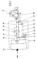
- IGBT and MOS-FET semiconductor are connected in parallel.
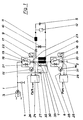
- Figure 1 shows the schematic view of a charger with IGBT and MOS-FET power transistors in the manner of an asymmetrical half-bridge.
- a DC voltage is supplied to the input connections 1, 2 from the network, specifically via a rectifier 3, which is also followed by a smoothing capacitor 4.
- a rectifier 3 which is also followed by a smoothing capacitor 4.
- a power transformer 6 With the power input and the consumer, in this case a battery 5, there is electrical isolation by a power transformer 6 with the two windings 7 - input winding - and 8 - output winding.
- a known rectifier and smoothing circuit with rectifier diode 9, free-wheeling diode 10 and choke 11 is connected to the output winding 8 and determines the contact resistance.
- Resistor 12 represents the internal resistance of the battery.
- the input winding 7 is connected between 1 and 2 via two circuit arrangements 13 and 14.
- These circuit arrangements consist of a direct parallel connection of an IGBT power semiconductor 15 and 16 and a MOS-FET power semiconductor 17 and 18.
- a relief circuit 19, 20 is arranged in parallel in the parallel circuit. This is known per se. It consists of a parallel connection of a diode 21 with a resistor 22 and a capacitor 23 in series therewith. The same applies to the relief circuit 20.
- Each parallel connection is controlled by a driver 24, 25.
- This driver has a connection 26, 27 to the control electrode of the IGBT power semiconductor 15, 16 and a further connection 28, 29 to the control electrode of the MOS-FET power semiconductor 17, 18.
- the circuit still has freewheeling diodes 32, 33 in the usual way, which allow current to pass in a certain manner when switched off.
- the assigned driver 24 - the same applies to the driver 25 in connection with the circuit arrangement 14 - has a galvanically isolated connection 34 and at the output a resistance circuit comprising three resistors 35, 36, 37 having.
- the resistor 35 is arranged in the connection 26 and the resistor 36 in the connection 28.
- the resistors 35, 36 have a low resistance, while the resistor 37 is provided in order to bring about a somewhat higher switch-off resistance at the connection 28.
- the gate voltage limitation in particular also a negative bias, is achieved by the diode circuit 38 with the three Diodes 39, 40, 41 and the capacitor 42 made.
- wiring resistors 44 to connection 28 and 45 to connection 26 are arranged between the line 43 from the capacitor 42 or a switch-on point (ground) between the diodes 40, 41.
- a different switch-off time is determined by this resistance circuit in connection with the power semiconductors, in any case only in the various capacitances present in the area of the switch-on electrode, the switch-off time of the MOS-FET semiconductor in particular being delayed.
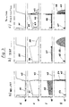
- FIG. shows a schematic representation of three pillars a, b and c.
- Column a shows the MOS-FET semiconductor
- column b the IGBT semiconductor
- column c the parallel connection
- ordinate 46 shows the voltage.
- ordinate 47 indicates the current.
- ordinate 48 shows the transmission losses during the passage of current.
- ordinate 49 shows the switching losses.
- the voltage ordinate is calibrated in volts, the ordinate 46 showing a voltage of the order of magnitude of 300 V at its upper limit on the characteristic curve on the left.
- the current in amperes in ordinate 47 indicates in the pass range from approximately 10 A to 15 A.
- Line f shows the forward losses in watts.
- the order of magnitude is from 100 W to 150 W.
- the switching losses are also given in watts in the ordinate.
- the upper limits, which are specified, are of the order of 100 W / SKT for a very short time.
- the MOS-FET semiconductor has a high current permeability with high transmission losses, but has very little switching loss. The latter results from the short switching time and thus from the steep voltage and current rise in lines d and e.
- the voltage characteristic curve 61 according to line d goes back to very low values (like IGBT 55), with a gradual increase when switched off.
- the current characteristic according to line e is important.
- the current according to the characteristic curve after 63 essentially passes through the IGBT semiconductor, the current in the MOS-FET semiconductor falls back to the characteristic curve 62, so that ultimately the remaining characteristic curve, the is drawn in dashed lines, corresponding to the course 64 arises.
- the trailing current drop according to curve 58 in column b decreases to a much lower value according to curve 65. It can therefore be seen from line f that the transmission losses 66 decrease to a very low value compared to 52 and also to a lower value compared to 57.
- the switching losses 67, 68, 69 according to row g may now be somewhat larger compared to column a; however, they are significantly smaller than according to pillar b, whereby this significant reduction, in which 68 corresponds to the proportion 54 in pillar a and 69 to the proportion 59 in pillar b, is mainly accompanied by the very low passage loss 66.
- This is the essential feature from column c and row e from the course of the characteristic curves 62 and 63 it can be seen that the two semiconductors are switched off at different times, which is essential for the embodiment described.
- a high on resistance (Rdson) reduces the forward current load.
- the required high voltage strength and the associated high Rdson values are an ideal combination.
- the forward power loss in the parallel MOS-FET semiconductor is kept as low as possible in this way.
- the MOS-FET current can be as large as the balance of the total power loss allows.
- the basic load is therefore relatively constant.
- the MOS-FET briefly carries a pulse current in order to relieve the IGBT.
- the voltage rises to the MOS-FET forward voltage, then delayed by the set time to the reverse voltage.
- the relatively high voltage drop across the MOS-FET power semiconductor generates a short-term pulse load, which, however, is significantly less than the turn-off losses of the IGBT (current tail at full reverse voltage).
- the maximum pulse load can be found in the MOS-FET diagram.
- the circuit of the device thus enables the use of the IGBT components for a much higher frequency range with cost advantages.
- the frequency limit is approx. Five times higher and the RCD protection circuit can become significantly smaller than if only IGBT was used.
- a parallel connection of several MOS-FET transistors can be replaced by a parallel IGBT transistor at a much lower cost, which additionally achieves a more favorable power loss balance.
Landscapes
- Engineering & Computer Science (AREA)
- Power Engineering (AREA)
- Dc-Dc Converters (AREA)
- Electronic Switches (AREA)
- Power Conversion In General (AREA)
- Input Circuits Of Receivers And Coupling Of Receivers And Audio Equipment (AREA)
Claims (3)
- Dispositif de commutation haute fréquence destiné à moduler une grandeur électrique, en liaison avec un transformateur ou un moteur comportant au moins un circuit en parallèle raccordé à une source de courant et contenant deux semi-conducteurs de puissance, l'un de ces semi-conducteurs étant un semi-conducteur MOSFET et les deux semi-conducteurs étant commandés de telle façon que le semi-conducteur MOSFET se bloque avec temporisation par rapport à l'autre semi-conducteur,
caractérisé en ce que l'autre semi-conducteur est un transistor IGBT (15, 16), en ce que le MOSFET (17, 18) présente une résistance (Rds on) d'enclenchement relativement élevée, en ce qu'il est prévu un seul organe de commande (24, 25) dont les signaux de commande sont émis, par l'intermédiaire de résistances (35, 36, 37) montées en parallèle, vers les électrodes de commande des semi-conducteurs (15, 16; 17, 18), la tension de blocage pour le MOSFET (17, 18) étant temporisée et le courant traversant le MOSFET (17, 18) étant essentiellement plus faible que le courant total traversant le montage en parallèle des semi-conducteurs (15, 16; 17, 18). - Dispositif de commutation suivant la revendication 1, caractérisé en ce que la résistance (35) conduisant le signal de commande destiné au IGBT (15, 16) et la résistance (37) conduisant le signal de déclenchement destiné au MOSFET (17, 18) sont dimensionnées en fonction de la capacité des semi-conducteurs (15, 16; 17, 18).
- Dispositif de commutation suivant la revendication 1 ou la revendication 2, caractérisé en ce que la tension Grille-Source sur le MOSFET (17, 18) est telle que le courant traversant le MOSFET est sensiblement inférieure à la moitié du courant nominal global traversant le montage en parallèle des semi-conducteurs (15, 16; 17, 18).
Applications Claiming Priority (2)
| Application Number | Priority Date | Filing Date | Title |
|---|---|---|---|
| DE4005168A DE4005168C2 (de) | 1990-02-17 | 1990-02-17 | Stromrichter für höhere Frequenzen |
| DE4005168 | 1990-02-17 |
Publications (2)
| Publication Number | Publication Date |
|---|---|
| EP0443155A1 EP0443155A1 (fr) | 1991-08-28 |
| EP0443155B1 true EP0443155B1 (fr) | 1995-01-25 |
Family
ID=6400489
Family Applications (1)
| Application Number | Title | Priority Date | Filing Date |
|---|---|---|---|
| EP90124484A Expired - Lifetime EP0443155B1 (fr) | 1990-02-17 | 1990-12-18 | Appareillage électrique pour enclencher et déclencher |
Country Status (3)
| Country | Link |
|---|---|
| EP (1) | EP0443155B1 (fr) |
| AT (1) | ATE117858T1 (fr) |
| DE (2) | DE4005168C2 (fr) |
Cited By (3)
| Publication number | Priority date | Publication date | Assignee | Title |
|---|---|---|---|---|
| CN101651420A (zh) * | 2008-08-15 | 2010-02-17 | 电力集成公司 | 非对称式开关正激变换器 |
| EP3012977A1 (fr) | 2014-10-24 | 2016-04-27 | ABB Technology AG | Procédé pour commuter un module semi-conducteur, module semi-conducteur et circuit en demi-pont |
| EP3057232A1 (fr) | 2015-02-10 | 2016-08-17 | ABB Technology AG | Dispositif de coupe-circuit |
Families Citing this family (14)
| Publication number | Priority date | Publication date | Assignee | Title |
|---|---|---|---|---|
| GB9104482D0 (en) * | 1991-03-04 | 1991-04-17 | Cooperheat Int Ltd | Solid state dc power supply |
| FR2680925B1 (fr) * | 1991-08-27 | 1993-12-17 | Sextant Avionique | Interrupteur statique a faibles pertes. |
| US5399908A (en) * | 1992-06-26 | 1995-03-21 | Kollmorgen Corporation | Apparatus and method for forced sharing of parallel MOSFET switching losses |
| GB2277215B (en) * | 1993-04-16 | 1997-04-23 | Marconi Gec Ltd | A power control switch |
| FR2740631B1 (fr) * | 1995-10-31 | 1998-01-16 | Eurofeedback Sa | Alimentation a haute tension et de forte puissance |
| EP1028528B1 (fr) * | 1998-08-28 | 2005-05-04 | Matsushita Electric Industrial Co., Ltd. | Regulateur de commutation et systeme lsi |
| WO2002061929A2 (fr) | 2001-01-30 | 2002-08-08 | True Solar Autonomy Holding B.V. | Circuit convertisseur de tension |
| DE10250154B4 (de) * | 2002-10-28 | 2007-05-03 | Infineon Technologies Ag | Schaltereinheit für ein Schaltnetzteil |
| DE10255373A1 (de) * | 2002-11-27 | 2004-06-24 | Siemens Ag | Vorrichtung zum elektronischen Schalten eines Lastelements, Anordnung der Vorrichtung und Verwendung der Vorrichtung bzw. Anordnung |
| EP2117121A1 (fr) * | 2008-05-06 | 2009-11-11 | Schleifring und Apparatebau GmbH | Commutateur d'alimentation à semi-conducteur |
| WO2016062426A1 (fr) | 2014-10-24 | 2016-04-28 | Abb Technology Ag | Module à semiconducteur et agencement de pile de modules à semiconducteurs |
| DE102014226475B3 (de) | 2014-12-18 | 2016-05-12 | Airbus Defence and Space GmbH | Gleichstromschaltvorrichtung und Verfahren zur Steuerung |
| DE102016201504A1 (de) | 2016-02-01 | 2017-08-03 | Bayerische Motoren Werke Aktiengesellschaft | Verbesserter Stromrichter |
| EP4064547A1 (fr) * | 2021-03-24 | 2022-09-28 | Siemens Gamesa Renewable Energy Innovation & Technology S.L. | Dispositif convertisseur de puissance multiniveau |
Family Cites Families (6)
| Publication number | Priority date | Publication date | Assignee | Title |
|---|---|---|---|---|
| US3878445A (en) * | 1972-09-01 | 1975-04-15 | Kearney & Trecker Corp | A. C. motor control apparatus and method |
| DE3508267A1 (de) * | 1985-03-08 | 1986-09-11 | Deutsche Thomson-Brandt Gmbh, 7730 Villingen-Schwenningen | Ablenk-netzteil-konzept fuer fersehgeraete |
| NO159898C (no) * | 1985-12-19 | 1989-02-15 | Alcatel Stk As | Stroemforsyning. |
| FR2614154A1 (fr) * | 1987-04-17 | 1988-10-21 | Thomson Semiconducteurs | Reseau d'aide a la commutation d'un transistor bipolaire de puissance |
| US4809148A (en) * | 1987-10-21 | 1989-02-28 | British Columbia Telephone Company | Full-fluxed, single-ended DC converter |
| US4864479A (en) * | 1988-03-07 | 1989-09-05 | General Electric Company | Full-bridge lossless switching converter |
-
1990
- 1990-02-17 DE DE4005168A patent/DE4005168C2/de not_active Expired - Fee Related
- 1990-12-18 EP EP90124484A patent/EP0443155B1/fr not_active Expired - Lifetime
- 1990-12-18 AT AT90124484T patent/ATE117858T1/de not_active IP Right Cessation
- 1990-12-18 DE DE59008364T patent/DE59008364D1/de not_active Expired - Fee Related
Cited By (4)
| Publication number | Priority date | Publication date | Assignee | Title |
|---|---|---|---|---|
| CN101651420A (zh) * | 2008-08-15 | 2010-02-17 | 电力集成公司 | 非对称式开关正激变换器 |
| CN101651420B (zh) * | 2008-08-15 | 2013-09-18 | 电力集成公司 | 非对称式开关正激变换器 |
| EP3012977A1 (fr) | 2014-10-24 | 2016-04-27 | ABB Technology AG | Procédé pour commuter un module semi-conducteur, module semi-conducteur et circuit en demi-pont |
| EP3057232A1 (fr) | 2015-02-10 | 2016-08-17 | ABB Technology AG | Dispositif de coupe-circuit |
Also Published As
| Publication number | Publication date |
|---|---|
| DE4005168A1 (de) | 1991-08-22 |
| EP0443155A1 (fr) | 1991-08-28 |
| ATE117858T1 (de) | 1995-02-15 |
| DE4005168C2 (de) | 1993-09-30 |
| DE59008364D1 (de) | 1995-03-09 |
Similar Documents
| Publication | Publication Date | Title |
|---|---|---|
| EP0443155B1 (fr) | Appareillage électrique pour enclencher et déclencher | |
| DE3126525C2 (de) | "Spannungsgesteuerter Halbleiterschalter und damit versehene Spannungswandlerschaltung" | |
| DE2834512C2 (de) | Umformer mit ausschaltbaren Thyristoren | |
| DE3623306A1 (de) | Entladungslampen-treiber | |
| CH700697A2 (de) | Schalteinrichtung mit einer kaskodeschaltung. | |
| DE19746112A1 (de) | Stromrichteranordnung | |
| EP0620957B1 (fr) | Circuit de protection d'un transistor de puissance mos a effet de champ | |
| EP2709257A2 (fr) | Circuit de convertisseur de courant et procédé de commande du circuit de convertisseur de courant | |
| EP1529336A1 (fr) | Convertisseur de commutation | |
| DE2809439A1 (de) | Schaltungseinrichtung zur steuerung des basisstromes eines als schalttransistor betriebenen leistungstransistors | |
| DE10231158A1 (de) | Gleichspannungswandler | |
| DE10328782B4 (de) | Steuerschaltung für einen MOSFET zur Synchrongleichrichtung | |
| DE4421249A1 (de) | Schaltstromversorgungsgerät mit Snubber-Schaltung | |
| EP1094605B1 (fr) | Montage servant à commander une charge à rayonnement parasite réduit | |
| DE102005027442B4 (de) | Schaltungsanordnung zum Schalten einer Last | |
| EP1071210A2 (fr) | Montage de circuit | |
| DE102006038474A1 (de) | Stromrichter | |
| EP0373240A1 (fr) | Circuit d'attaque auto-régulé avec régulation du degré de saturation pour le courant de base d'un transistor de puissance | |
| EP3997790B1 (fr) | Ensemble circuit servant à commuter des éléments de commutation | |
| EP0792538A1 (fr) | Circuit destine a l'utilisation multiple d'un noyau de transformateur | |
| DE69534510T2 (de) | Ansteuereinrichtung eines Hochstromschalters mit isoliertem Gate und Impulsschalter unter Verwendung derselben | |
| EP0590167A1 (fr) | Commutateur de puissance | |
| DE9302756U1 (de) | Rückkopplungsregler | |
| EP0163299A1 (fr) | Circuit de convertisseur avec un transformateur | |
| DE102007042084A1 (de) | Schaltwandler mit Mehrfachausgang und Ausgangsspannungsregelung |
Legal Events
| Date | Code | Title | Description |
|---|---|---|---|
| PUAI | Public reference made under article 153(3) epc to a published international application that has entered the european phase |
Free format text: ORIGINAL CODE: 0009012 |
|
| 17P | Request for examination filed |
Effective date: 19901224 |
|
| AK | Designated contracting states |
Kind code of ref document: A1 Designated state(s): AT CH DE FR GB IT LI SE |
|
| 17Q | First examination report despatched |
Effective date: 19930623 |
|
| GRAA | (expected) grant |
Free format text: ORIGINAL CODE: 0009210 |
|
| AK | Designated contracting states |
Kind code of ref document: B1 Designated state(s): AT CH DE FR GB IT LI SE |
|
| REF | Corresponds to: |
Ref document number: 117858 Country of ref document: AT Date of ref document: 19950215 Kind code of ref document: T |
|
| EAL | Se: european patent in force in sweden |
Ref document number: 90124484.8 |
|
| REF | Corresponds to: |
Ref document number: 59008364 Country of ref document: DE Date of ref document: 19950309 |
|
| ITF | It: translation for a ep patent filed | ||
| ET | Fr: translation filed | ||
| GBT | Gb: translation of ep patent filed (gb section 77(6)(a)/1977) |
Effective date: 19950427 |
|
| PLBE | No opposition filed within time limit |
Free format text: ORIGINAL CODE: 0009261 |
|
| STAA | Information on the status of an ep patent application or granted ep patent |
Free format text: STATUS: NO OPPOSITION FILED WITHIN TIME LIMIT |
|
| 26N | No opposition filed | ||
| PGFP | Annual fee paid to national office [announced via postgrant information from national office to epo] |
Ref country code: AT Payment date: 19961128 Year of fee payment: 7 |
|
| PGFP | Annual fee paid to national office [announced via postgrant information from national office to epo] |
Ref country code: CH Payment date: 19961129 Year of fee payment: 7 |
|
| PGFP | Annual fee paid to national office [announced via postgrant information from national office to epo] |
Ref country code: SE Payment date: 19961202 Year of fee payment: 7 |
|
| PGFP | Annual fee paid to national office [announced via postgrant information from national office to epo] |
Ref country code: GB Payment date: 19961209 Year of fee payment: 7 |
|
| PGFP | Annual fee paid to national office [announced via postgrant information from national office to epo] |
Ref country code: FR Payment date: 19961219 Year of fee payment: 7 |
|
| PGFP | Annual fee paid to national office [announced via postgrant information from national office to epo] |
Ref country code: DE Payment date: 19970211 Year of fee payment: 7 |
|
| PG25 | Lapsed in a contracting state [announced via postgrant information from national office to epo] |
Ref country code: GB Free format text: LAPSE BECAUSE OF NON-PAYMENT OF DUE FEES Effective date: 19971218 Ref country code: AT Free format text: LAPSE BECAUSE OF NON-PAYMENT OF DUE FEES Effective date: 19971218 |
|
| PG25 | Lapsed in a contracting state [announced via postgrant information from national office to epo] |
Ref country code: SE Free format text: LAPSE BECAUSE OF NON-PAYMENT OF DUE FEES Effective date: 19971219 |
|
| PG25 | Lapsed in a contracting state [announced via postgrant information from national office to epo] |
Ref country code: LI Free format text: LAPSE BECAUSE OF NON-PAYMENT OF DUE FEES Effective date: 19971231 Ref country code: FR Free format text: THE PATENT HAS BEEN ANNULLED BY A DECISION OF A NATIONAL AUTHORITY Effective date: 19971231 Ref country code: CH Free format text: LAPSE BECAUSE OF NON-PAYMENT OF DUE FEES Effective date: 19971231 |
|
| GBPC | Gb: european patent ceased through non-payment of renewal fee |
Effective date: 19971218 |
|
| REG | Reference to a national code |
Ref country code: CH Ref legal event code: PL |
|
| PG25 | Lapsed in a contracting state [announced via postgrant information from national office to epo] |
Ref country code: DE Free format text: LAPSE BECAUSE OF NON-PAYMENT OF DUE FEES Effective date: 19980901 |
|
| EUG | Se: european patent has lapsed |
Ref document number: 90124484.8 |
|
| REG | Reference to a national code |
Ref country code: FR Ref legal event code: ST |
|
| PG25 | Lapsed in a contracting state [announced via postgrant information from national office to epo] |
Ref country code: IT Free format text: LAPSE BECAUSE OF NON-PAYMENT OF DUE FEES;WARNING: LAPSES OF ITALIAN PATENTS WITH EFFECTIVE DATE BEFORE 2007 MAY HAVE OCCURRED AT ANY TIME BEFORE 2007. THE CORRECT EFFECTIVE DATE MAY BE DIFFERENT FROM THE ONE RECORDED. Effective date: 20051218 |