EP3057232A1 - Dispositif de coupe-circuit - Google Patents
Dispositif de coupe-circuit Download PDFInfo
- Publication number
- EP3057232A1 EP3057232A1 EP15154508.4A EP15154508A EP3057232A1 EP 3057232 A1 EP3057232 A1 EP 3057232A1 EP 15154508 A EP15154508 A EP 15154508A EP 3057232 A1 EP3057232 A1 EP 3057232A1
- Authority
- EP
- European Patent Office
- Prior art keywords
- switch
- arrangement
- circuit breaker
- breaker device
- switch arrangement
- Prior art date
- Legal status (The legal status is an assumption and is not a legal conclusion. Google has not performed a legal analysis and makes no representation as to the accuracy of the status listed.)
- Withdrawn
Links
- 239000004065 semiconductor Substances 0.000 claims abstract description 111
- XUIMIQQOPSSXEZ-UHFFFAOYSA-N Silicon Chemical compound [Si] XUIMIQQOPSSXEZ-UHFFFAOYSA-N 0.000 claims abstract description 73
- 229910052710 silicon Inorganic materials 0.000 claims abstract description 73
- 239000010703 silicon Substances 0.000 claims abstract description 73
- 238000000034 method Methods 0.000 claims abstract description 13
- 230000000903 blocking effect Effects 0.000 claims description 33
- 230000002457 bidirectional effect Effects 0.000 claims description 24
- HBMJWWWQQXIZIP-UHFFFAOYSA-N silicon carbide Chemical compound [Si+]#[C-] HBMJWWWQQXIZIP-UHFFFAOYSA-N 0.000 claims description 22
- 229910010271 silicon carbide Inorganic materials 0.000 claims description 19
- JMASRVWKEDWRBT-UHFFFAOYSA-N Gallium nitride Chemical compound [Ga]#N JMASRVWKEDWRBT-UHFFFAOYSA-N 0.000 claims description 6
- 229910002601 GaN Inorganic materials 0.000 claims description 4
- 230000008901 benefit Effects 0.000 description 7
- 239000000463 material Substances 0.000 description 4
- 230000001419 dependent effect Effects 0.000 description 2
- 230000005669 field effect Effects 0.000 description 2
- 230000004888 barrier function Effects 0.000 description 1
- 230000005684 electric field Effects 0.000 description 1
Images


Classifications
-
- H—ELECTRICITY
- H03—ELECTRONIC CIRCUITRY
- H03K—PULSE TECHNIQUE
- H03K17/00—Electronic switching or gating, i.e. not by contact-making and –breaking
- H03K17/08—Modifications for protecting switching circuit against overcurrent or overvoltage
- H03K17/081—Modifications for protecting switching circuit against overcurrent or overvoltage without feedback from the output circuit to the control circuit
- H03K17/08116—Modifications for protecting switching circuit against overcurrent or overvoltage without feedback from the output circuit to the control circuit in composite switches
-
- H—ELECTRICITY
- H03—ELECTRONIC CIRCUITRY
- H03K—PULSE TECHNIQUE
- H03K17/00—Electronic switching or gating, i.e. not by contact-making and –breaking
- H03K17/12—Modifications for increasing the maximum permissible switched current
- H03K17/127—Modifications for increasing the maximum permissible switched current in composite switches
-
- H—ELECTRICITY
- H03—ELECTRONIC CIRCUITRY
- H03K—PULSE TECHNIQUE
- H03K17/00—Electronic switching or gating, i.e. not by contact-making and –breaking
- H03K17/51—Electronic switching or gating, i.e. not by contact-making and –breaking characterised by the components used
- H03K17/56—Electronic switching or gating, i.e. not by contact-making and –breaking characterised by the components used by the use, as active elements, of semiconductor devices
- H03K17/567—Circuits characterised by the use of more than one type of semiconductor device, e.g. BIMOS, composite devices such as IGBT
-
- H—ELECTRICITY
- H03—ELECTRONIC CIRCUITRY
- H03K—PULSE TECHNIQUE
- H03K2217/00—Indexing scheme related to electronic switching or gating, i.e. not by contact-making or -breaking covered by H03K17/00
- H03K2217/0009—AC switches, i.e. delivering AC power to a load
Definitions
- the invention relates to the field of power semiconductor electronics.
- the invention relates to a circuit breaker device employing a power semiconductor device and to a method for interrupting a current flow in an electrical circuit.
- Wide bandgap semiconductor switches may generally permit energy efficient operation at considerably high voltages, frequencies and/or temperatures compared to conventional semiconductor switches, such as e.g. bipolar silicon (Si) based semiconductor switches.
- bipolar silicon-based switches such as e.g. insulated gate bipolar transistors (IGBT), reverse conducting insulated gate bipolar transistors (RC-IGBT), and bi-mode insulated gate transistors (BIGT), may further provide various advantages compared to wide bandgap switches.
- bipolar Si based switches may provide good protection characteristics including high current and series connection high voltage capability, a reliable short circuit failure mode, good short circuit capability due to a relatively high saturation current and good surge current capability in diode mode.
- US 2014/0185346 A1 relates to a hybrid power device comprising first and second switching devices containing first and second unequal band-gap semiconductor materials, wherein the switching devices are three or more terminal switching devices of different type.
- EP 0 443 155 B1 relates to a switchgear employing MOS-FET semiconductors, which are connected in parallel and switchable at high frequencies, and IGBT power semiconductors.
- An aspect of the invention relates to a circuit breaker device for interrupting a current flow in an electrical circuit, wherein the current flow may be reversibly interrupted by means of the inventive circuit breaker device.
- the inventive circuit breaker device may be utilized for interrupting a flow of alternating current (AC) and/or a flow of direct current (DC).
- the circuit breaker device comprises a first switch arrangement comprising a first silicon-based semiconductor switch and a second silicon-based semiconductor switch, which first silicon-based semiconductor switch and second silicon-based semiconductor switch are antisymmetrically interconnected with each other.
- the circuit breaker device further comprises a second switch arrangement comprising a first wide bandgap (WBG) semiconductor switch and a second wide bandgap semiconductor switch, which first wide bandgap semiconductor switch and second wide bandgap semiconductor switch are connected in series in a back-to-back arrangement.
- WBG wide bandgap
- the first switch arrangement is arranged in parallel to the second switch arrangement.
- first silicon-based semiconductor switch first semiconductor switch
- second silicon-based semiconductor switch second semiconductor switch
- second silicon switch second semiconductor switch
- first wide bandgap semiconductor switch first wide bandgap switch
- second wide bandgap semiconductor switch second wide bandgap switch
- antisymmetric interconnection of the first and second semiconductor switches may refer to an antiparallel arrangement and/or interconnection of the first and second semiconductor switches, and/or the term may refer to a series connection of the first and second semiconductor switches in a back-to-back arrangement.
- back-to-back may mean that a terminal of one type of a first switch is interconnected with a terminal of the same type of a second switch.
- a source terminal of a first switch is connected to a source terminal of a second switch, or a drain terminal of a first switch is connected to a drain terminal of the second switch, or an emitter terminal of a first switch is connected to an emitter terminal of a second switch, or a collector terminal of a first switch is connected to a collector terminal of a second switch.
- a cathode terminals or anode terminals of two switches may be interconnected, for instance in case of thyristors.
- the respective terminals of the first and second switch may either be directly connected, i.e. they may be in direct contact, or they may be connected via some electrically conductive connection element.
- wide bandgap may refer to a semiconductor material, in which the bandgap, i.e. the respective energy difference between valence and conduction band, may be larger than 3 eV.
- a hybrid combination, and/or hybrid arrangement, and/or hybrid device of a silicon-based semiconductor switch and a WBG switch in parallel may generally be listed in terms of overall performance and cost compared to a full WBG device, i.e. a device employing solely WBG switches, and/or compared to a full silicon device, i.e. a device employing solely silicon-based semiconductor switches.
- a hybrid combination of a silicon-based semiconductor switch such as e.g. an insulated gate bipolar transistor (IGBT) and/or a reverse conducting IGBT
- a WBG switch such as e.g. a voltage controlled unipolar switch
- a WBG switch such as e.g. a voltage controlled unipolar switch
- An advantageous feature of such hybrid combination may be to reduce cost by using a minimum number of WBG devices, while maintaining the performance advantages provided by these WBG devices.
- switching losses may be regarded a minor issue since switching events for interrupting the current flow in the circuit may usually be single events. Accordingly, a reduction of switching losses by using a hybrid combination or a hybrid device may only bring considerably minor benefits.
- the inventive circuit breaker device employing a hybrid combination of Si-based semiconductor switches and WBG switches may advantageously provide low conduction losses under a full current range, for which the circuit breaker device may be utilized. This may allow the inventive circuit breaker device to compete with mechanical solutions for circuit breaker devices. Moreover, the inventive circuit breaker device may provide high breaking current turn-off capability for the switching events, i.e. the events in which the current flow in the circuit may be interrupted by means of the circuit breaker device. Although silicon-based bipolar semiconductor devices may provide comparable performance, they may not provide low conduction losses at low current due to the inherent built-in voltage of Silicon of around 0.7 V for forward biasing a p-n junction of the silicon-based switch.
- unipolar switches such as Metal-Oxide-Semiconductor Field-Effect Transistors (MOSFETs)
- MOSFETs Metal-Oxide-Semiconductor Field-Effect Transistors
- WBG switches such as e.g. a Silicon-Carbide (SiC) MOSFET
- SiC Silicon-Carbide
- unipolar WBG switches may always have the drawback of lacking surge current capability when compared to bipolar silicon-based switches.
- the inventive circuit breaker device may be regarded as a cross switch hybrid arrangement of silicon-based semiconductor switches and WBG switches connected in parallel. As may be desired for circuit breaker applications, the inventive circuit breaker device may advantageously provide bidirectional functionality with low (conduction) losses over the full current range, in which such circuit breaker devices may usually be applicable, combined with high turn-off current capabilities, while additionally providing surge current capabilities.
- a further aspect of the invention relates to a method for interrupting a current flow in an electrical circuit with a circuit breaker device
- features of the method as described in the above and in the following may be features of the circuit breaker device as described in the above and in the following.
- features of the circuit breaker device may be features of the method.
- the first switch arrangement provides full bidirectionality and/or the first switch arrangement is a fully bidirectional switch arrangement.
- the second switch arrangement provides full bidirectionality and/or the second switch arrangement is a fully bidirectional arrangement.
- full bidirectionality may comprise bidirectional conduction capability, bidirectional blocking capability and/or bidirectional control capability of the first and/or second switch arrangement.
- the first switch arrangement may comprise a conducting state, in which a current through the first switch arrangement may be conductable in two directions and/or may be bidirectionally conductable, and a blocking state, in which the current through the first switch arrangement may be blockable in two directions and/or may be bidirectionally blockable.
- the second switch arrangement may comprise an on-state, in which a current through the second switch arrangement may be conductable in two directions and/or may be bidirectionally conductable, and an off-state, in which the current through the second switch arrangement may be blockable in two directions and/or may be bidirectionally blockable.
- the first switch arrangement comprises at least one of an insulated gate bipolar transistor (IGBT), a diode, a reverse conducting insulated gate bipolar transistor (RC-IGBT), an integrated gate-commutated thyristor (IGCT), a reverse blocking integrated gate-commutated thyristor (RB-IGCT), a bi-mode insulated gate transistor (BIGT), a bidirectional thyristor, and a bidirectional turn-off thyristor.
- the bidirectional turn-off thyristor may refer to a bipolar gate turn-off thyristor.
- Either of these semiconductor switches may comprise at least one internal diode, which internal diode may be reverse conducting or reverse blocking.
- the first and second semiconductor switches may both be IGBTs, optionally comprising an internal or external diode, which diode may be a reverse conducting diode; the first and second semiconductor switches may both be RC-IGBTs; the first and second semiconductor switches may both be RB-IGCTs; the first and second semiconductor switches may both be bidirectional thyristors and/or bidirectional turn-off thyristors.
- the first semiconductor switch and the second semiconductor switch of the first switch arrangement are reverse blocking switches, wherein the first semiconductor switch and the second semiconductor switch of the first switch arrangement are arranged antiparallel with respect to each other.
- the first and/or the second semiconductor switch may each comprise an internal and/or an external reverse blocking diode, wherein an internal diode may be integrated in the respective semiconductor switch.
- two reverse blocking switches may be arranged antiparallel with respect to each other or two reverse conducting switches may be arranged and/or connected back-to-back in series.
- the antiparallel arrangement may provide full bidirectionality to the first switch arrangement, which in turn may be advantageous for circuit breaker applications, particularly for applications, in which an AC current in the electrical circuit is to be interrupted by means of the circuit breaker device.
- a back-to-back arrangement of series connected reverse conducting switches such as e.g. IGBTs, MOSFETs and/or other planar termination based switches
- conduction losses resulting from the series connection may be higher when compared to the antiparallel arrangement of two reverse blocking switches, since only one of the first and second semiconductor switches may be required per direction of current flow through the first switch arrangement.
- the antiparallel arrangement of the first and second reverse blocking semiconductor switches may reduce conduction losses and thus may improve an energy efficiency of the entire circuit breaker device.
- the first semiconductor switch is an RB-IGCT and the second semiconductor switch is an RB-IGCT arranged antiparallel to the first semiconductor switch.
- the first and/or second semiconductor switch may alternatively be bidirectional thyristors and/or bidirectional turn-off thyristors.
- RB-IGCTs may comprise a bipolar termination, e.g. with double sided bevels, and may advantageously improve the energy efficiency of the circuit breaker device by reducing conduction losses.
- the first semiconductor switch and the second semiconductor switch of the first switch arrangement are reverse conducting switches, wherein the first semiconductor switch and the second semiconductor switch are series connected in a back-to-back arrangement.
- an emitter terminal of the first semiconductor switch may be interconnected with an emitter terminal of the second semiconductor switch, either directly or indirectly by means of an electrically conductive element.
- the back-to-back arrangement of series connected reverse conducting switches may advantageously provide full bidirectionality to the first switch arrangement.
- Reverse conducting capability may be provided to each of the first and second semiconductor switches by means of an internal or an external diode.
- both the first and the second semiconductor switches may be IGBTs, each connected to an external reverse conducting diode to provide reverse conduction capability.
- both the first and second semiconductor switches may be RC-IGBTs, or the first semiconductor switch may be an IGBT with external reverse conducting diode and the second semiconductor switch may be an RC-IGBT.
- the first semiconductor switch and/or the second semiconductor switch of the first switch arrangement comprises an internal reverse conducting diode. This may render an external reverse conducting diode superfluous and may thus allow a compact design of the circuit breaker device.
- the first wide bandgap switch and the second wide bandgap switch of the second switch arrangement each have no built-in voltage and/or each have a built-in voltage of zero Volts.
- the first and second wide bandgap switches may lack a built-in voltage due to an absence of a pn junction and/or any other barrier type.
- the first and second wide bandgap switches may be e.g. unipolar semiconductor switches. This may further improve the energy efficiency of the circuit breaker device as low conduction losses may be achieved even at considerably low currents below e.g. 10 A.
- the first wide bandgap switch and the second wide bandgap switch of the second switch arrangement are voltage-controlled switches.
- the term "voltage controlled switch” may relate to a switch and/or semiconductor device, whose output characteristics are determined and/or controlled by an electrical field depending on the voltage applied to the gate terminal of the respective switch.
- a MOSFET, a junction-gate field-effect transistor (JFET), and/or a high electron mobility transistor (HEMT) may be utilized as wide band-gap switch.
- the first and the second WBG switches may be voltage-controlled unipolar switches.
- the first wide band-gap switch and/or the second wide band-gap switch is a MOSFET.
- the first wide band-gap switch and the second wide band-gap switch of the second switch arrangement are based on silicon carbide (SiC) and/or on gallium nitride (GaN).
- SiC silicon carbide
- GaN gallium nitride
- a SiC MOSFET and/or a GaN HEMT may be utilized as first and/or second wide bandgap switch.
- Such switches may particularly provide low losses at low currents.
- the current in the circuit is interruptable by switching the second switch arrangement to an off-state, in which at least one of the first and second wide bandgap switches is turned off, and by switching the first switch arrangement to a blocking state, in which at least one of the first semiconductor switch and the second semiconductor switch is blocking a current flow through the first switch arrangement.
- the second switch arrangement may be switched to the off-state by applying an appropriate gate signal to a gate terminal of at least one of the WBG switches, wherein the gate signal may be a positive/negative gate current signal or a positive/negative gate voltage signal, depending on the characteristic of the first and second WBG switches.
- the first switch arrangement may be switched to the blocking state by applying an appropriate gate signal to a gate terminal of at least one of the first and second semiconductor switches, wherein the gate signal may be a positive/negative gate current signal or a positive/negative gate voltage signal, depending on the characteristic of the first and second semiconductor switches.
- the second switch arrangement is switched to the off-state by applying a negative gate signal to a gate terminal of the first wide bandgap switch and/or to a gate terminal of the second wide bandgap switch.
- the gate signal may be a negative gate voltage signal applied to the SiC MOSFET's gate terminal in order to turn the switch off.
- a further aspect of the invention relates to a use of a first switch arrangement arranged parallel to a second switch arrangement in a circuit breaker device for interrupting a current flow in an electrical circuit.
- the first switch arrangement is a bidirectional switch arrangement comprising two silicon-based semiconductor switches
- the second switch arrangement is a back-to-back arrangement of at least two wide bandgap semiconductor switches connected in series.
- the two silicon-based semiconductor switches of the first switch arrangement may be connected antiparallel or they may be series connected back-to-back, as described in the above and in the following.
- Yet a further aspect of the invention relates to a method for interrupting a current flow in an electrical circuit with a circuit breaker device as described in the above and in the following.
- the method comprises the steps of switching the second switch arrangement to an off-state by applying a negative gate signal to a gate terminal of at least one of the first and second wide bandgap switch of the second switch arrangement, and switching the first switch arrangement to a blocking state by applying a turn-off gate signal to a gate terminal of at least one of the first and second semiconductor switches of the first switch arrangement.
- the second switch arrangement is switched to the off-state prior to switching the first switch arrangement to the blocking state by a predefined delay time. Switching the second switch arrangement to the off-state prior to switching the first switch arrangement to the blocking state may avoid damages to the second switch arrangement, as the first and second WBG switches may not be capable to carry excessive amounts of current.
- the delay time is in the range of 5 ⁇ s to 500 ⁇ s.
- the delay time may for example range from 10 ⁇ s to 100 ⁇ s, and preferably from 10 ⁇ s to 50 ⁇ s.
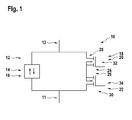
- Fig. 1 schematically shows a circuit breaker device 10 for interrupting a current flow in an electrical circuit according to an embodiment of the invention.
- the circuit breaker device 10 comprises an input 11 and an output 13 for connecting and/or integrating the circuit breaker device 10 in the electrical circuit, in which the current flow may be interrupted by means of the circuit breaker device 10.
- the circuit breaker device 10 comprises a first switch arrangement 12 arranged and/or connected in parallel to a second switch arrangement 18.
- the first switch arrangement 12 comprises a first silicon-based semiconductor switch 14 and a second silicon-based semiconductor switch 16.
- the first and the second silicon switches 14, 16 are antisymmetrically interconnected with each other and/or antisymmetrically arranged with respect to each other. This means the first and the second silicon switches 14, 16 may either be arranged and/or interconnected antiparallel or the first and second silicon switches 14, 16 may be series connected back-to-back.
- the first switch arrangement 12 is adapted for providing full bidirectionality in terms of conduction capability, blocking capability, and /or control capability. Accordingly, the first switch arrangement 12 comprises a conducting state, in which current may flow through the first switch arrangement 12 in both directions, i.e. from input 11 to output 13 or from output 13 to input 11. Further, the first switch arrangement 12 comprises a blocking state, in which the current flow through the first switch arrangement 12 may be blocked in both directions, i.e. from input 11 to output 13 and from output 13 to input 11.
- the actual arrangement of the first and second silicon switches 14, 16 may depend on their characteristics and/or specifications, as outlined above.
- the first and second silicon switches 14, 16 may be reverse conducting switches, the first and second silicon switches 14, 16 may be series connected back-to-back in order to provide full bidirectionality to the first switch arrangement 12.
- a reverse conducting capability may be provided to the first and/or second silicon switch 14, 16 e.g. by an internal diode integrated in the first and/or second silicon switch 14, 16 or by an external diode, which may be connected to the first and/or second silicon switch 14, 16, for instance by means of a conduction element.
- bidirectionality may be provided by arranging and/or interconnecting the first and the second silicon switches 14, 16 antiparallel with respect to each other.
- the first silicon switch 14 may be an IGBT with internal or external reverse conducting diode
- the second silicon switch 16 may be an IGBT with internal or external reverse conducting diode, wherein the first and second silicon switches 14, 16 are series connected back-to-back, i.e. a collector terminal of the first silicon switch 14 may be interconnected with a collector terminal of the second silicon switch 16.
- the respective collector terminals may be in direct contact or interconnected by means of a conduction element.
- both the first and the second silicon switches 14, 16 may be RC-IGBTs series connected back-to-back, with the respective collector terminals of the first and second silicon switches 14, 16 being interconnected.
- the first silicon switch 14 may be an IGBT with internal or external reverse conducting diode
- the second silicon switch 16 may be an RC-IGBT series connected back-to-back with the first silicon switch 14, the respective collector terminals of the first and second silicon switches 14, 16 being interconnected.
- both the first and the second silicon switch es14, 16 may be RB-IGCTs connected and/or arranged antiparallel with respect to each other, wherein a collector terminal of one of the first and the second silicon switches 14, 16 may be directly connected to and/or may be directed towards the input 11, whereas the collector terminal of the other one of the first and second silicon switches 14, 16 may be directly connected and/or may be directed towards the output 13.
- Both the first and the second silicon switches 14, 16 may be bidirectional (gate) turn-off thyristors connected and/or arranged antiparallel, wherein respective anodes of the first and the second silicon switches 14, 16 may be directed in opposite directions with respect to each other.
- Both the first and the second silicon switches 14, 16 may be bidirectional thyristors connected and/or arranged antiparallel, wherein respective anodes of the first and the second silicon switches 14, 16 may be directed in opposite directions with respect to each other.
- first silicon switch 14 may be a bidirectional thyristor and the second silicon switch 16 may be a bidirectional (gate) turn-off thyristor arranged antiparallel to the first silicon switch 14.
- first silicon switch 14 may be an RB-IGCT arranged antiparallel to the second silicon switch 16, which may be a bidirectional thyristor or a bidirectional (gate) turn-off thyristor.
- the second switch arrangement 18 of the circuit breaker device 10, which second switch arrangement 18 is parallel connected to the first switch arrangement 12, comprises a first wide bandgap (WBG) switch 20 and a second wide bandgap switch 22.
- the first and the second WBG switches 20, 22 are series connected back-to-back, wherein a source terminal 24 of the first WBG switch 20 is connected to a source terminal 26 of the second WBG switch 22.
- the source terminals 24, 26 may be directly connected, e.g. by direct contact of both source terminals 24, 26, or they may be connected via a conduction element.
- a drain terminal 28 of the first WBG switch 20 is connected to the output 13 and a drain terminal 30 of the second WBG switch is connected to the input 11.
- the first WBG switch 20 comprises a gate terminal 32 and the second WBG switch 22 comprises a gate terminal 34, allowing control of the corresponding first or second WBG switch 20, 22.
- Both gate terminals 32, 34 may be interconnected by means of a common gate unit of the second switch arrangement 18, thereby simplifying control of the second switch arrangement 18.
- the first and the second WBG switches 20, 22 may be voltage-controlled, and they may basically be unipolar or bipolar semiconductor switches, respectively. However, in order to achieve low conduction losses at low currents flowing through the second switch arrangement 18, e.g. currents below 10 A, it might be advantageous to design the first and the second WBG switches 20, 22 as unipolar voltage-controlled switches.
- the first and the second WBG switches 20, 22 may for instance be MOSFETs and/or HEMTs.
- the first and/or the second WBG switches 20, 22 may for instance be based on SiC and/or on GaN.
- both the first and the second WBG switches 20, 22 are SiC MOSFETs having no built-in voltage, thereby reducing conduction losses at low currents.
- the second switch arrangement 20 may be switched from an on-state, in which current may flow through the second switch arrangement 18 at least in one direction, to an off-state, in which a current flow through the second switch arrangement 18 may be blocked in at least one direction.
- the second switch arrangement 18 may be switched to the off-state by supplying a gate signal to at least one of the gate terminals 32, 34 of the first and/or second WBG switch 20, 22, which gate signal may be adapted for turning-off the corresponding first and/or second WBG switch 20, 22.
- Characteristics of the applied gate signal such as e.g.
- a signal strength, a signal voltage, a signal current and/or a signal sign may depend on the characteristics and specifications of the respective first and/or second WBG switch 20, 22.
- both the first and the second WBG switches 20, 22 are SiC MOSFETs they may be conducting and/or they may be turned-on if a positive gate voltage is applied to the respective gate terminal 32, 34 of the first and/or second WBG switch 20, 22.
- the first and/or second WBG switch 20, 22 may be turned-off by applying a negative voltage to the respective gate terminal 32, 34. Accordingly, for switching the second switch arrangement 18 to the off-state, a negative gate voltage signal may be applied to at least one of the first and the second WBG switch 20, 22, in order to interrupt current flowing through the second switch arrangement 18.
- the first switch arrangement 12 is switched to the blocking state, by applying at least one appropriate gate signal to a gate terminal of at least one of the first and the second silicon switches 14, 16 in order to turn-off the respective at least one of the first and the second silicon switch 14, 16. Also characteristics of this at least one gate signal may depend on the characteristics and specifications of the corresponding first and/or second silicon switch 14, 16.
- Fig. 2A schematically shows a circuit breaker device 10 according to an embodiment of the invention.
- Fig. 2B schematically shows forward characteristics of components of the circuit breaker device 10 of Fig. 2A .
- the circuit breaker device 10 of Fig. 2A may comprise the same elements, features and/or functions as the circuit breaker device of Fig. 1 .
- the circuit breaker device 10 comprises a first switch arrangement 12 with a first RB-IGCT 14 employed as first semiconductor switch connected and/or arranged antiparallel to a second RB-IGCT 16 employed as second semiconductor switch, thereby providing full bidirectionality to the first switch arrangement 12.
- the circuit breaker device 10 further comprises a second switch arrangement 18 connected in parallel to the first switch arrangement 12.
- the second switch arrangement 18 comprises a first SiC MOSFET 20 as first WBG switch and a second SiC MOSFET 22 as second WBG switch.
- the first and the second SiC MOSFETs 20, 22 are series connected back-to-back with their respective source terminals 24, 26 being interconnected.
- An operational mode of the circuit breaker device 10 may involve at least two separate gate units for the first switch arrangement 12 and the second switch arrangement 18. Accordingly, a gate terminal of the first RB-IGCT 14 and a gate terminal of the second RB-IGCT 16 may be connected to a first common gate unit for controlling the first switch arrangement 12, i.e. for controlling both the first and the second RB-IGCTs 14, 16. However, the gate terminals of the first and second RB-IGCTs 14, 16 may also be independently controlled. Further, the gate terminals 32, 34 of the first and second SiC MOSFETs 20, 22 may be connected to a second common gate unit for controlling the second switch arrangement 18, i.e. for controlling both the first and the second SiC MOSFETs 20, 22. However, the gate terminals 32, 34 may also be independently controlled.
- At least one of the first and second RB-IGCT 14, 16 may be forward biased and/or fired and/or switched into the conducting state while a positive gate voltage is applied on both gate terminals 32, 34 of the first and second SiC MOSFETs 20, 22, thereby switching the second switch arrangement 18 to the on-state.
- the on-state of the second switch arrangement 18 it may be benefitted from the bidirectional current capability of the MOSFET structure of each of the first and second SiC MOSFETs 20, 22, wherein it may not be required to use and/or switch at least one of an internal MOSFET Positive-Intrinsic-Negative (PIN) diode to be conducting.
- PIN Positive-Intrinsic-Negative
- a negative gate voltage signal is applied to at least one of the gate terminals 32, 34 of the first and second SiC MOSFET 20, 22, and/or a negative voltage signal is applied to the second common gate unit of the second switch arrangement 14.
- the negative voltage signal applied at least one of the first and the second SiC MOSFET 20, 22 is turned-off, the second switch arrangement 14 is switched to the off-state and any current may solely flow through the first switch arrangement 12.
- a turn-off gate signal is applied to at least one of the gate terminals of the first and second RB-IGCTs 14, 16 and/or to the first common gate unit of the first switch arrangement 12.
- the first switch arrangement 12 is switched to the blocking state, thereby blocking current flow through the first switch arrangement 12, and thereby blocking current flow between input 11 and output 13 and blocking current flow in the electrical circuit connected to input 11 and/or output 13.
- the turn-off gate signal applied to the first switch arrangement 12 may for instance be a negative gate voltage signal.
- the second switch arrangement 18 is switched to the off-state prior to switching the first switch arrangement 12 to the blocking state in order to avoid potential damage to the second switch arrangement 18 if all current would be channelled through the second switch arrangement 18.
- the first switch arrangement 12 may be switched to the blocking state after a predefined and/or defineable delay time after switching the second switch arrangement 18 to the off-state.
- the delay time may be in the range of 5 ⁇ s to 500 ⁇ s, preferably in the range of 10 ⁇ s to 50 ⁇ s.
- Fig. 2B the advantages of the inventive circuit breaker device 10 are clearly visible.
- voltage drops of the first switch arrangement 12, of the second switch arrangement 18, and of the parallel connected first and second switch arrangements 12, 18, i.e. of the circuit breaker device 10 are shown as a function of the current applied, i.e. on-state curves 36, 38, 40 of the respective devices are shown.
- the x-axis refers to the voltage drop in Volts and the y-axis refers to the applied current in Ampere, wherein both the x-axis and the y-axis are shown in log-scale.
- Curve 36 corresponds to the forward characteristics of the first switch arrangement 12 with two antiparallel RB-IGCTs 14, 16 curve 38 corresponds to the forward characteristics of the second switch arrangement 18 with two series back-to-back connected SiC MOSFETs 20, 22, and curve 40 corresponds to the parallel arrangement of the first and second switch arrangements 12, 18, which may be regarded as full cross hybrid switch.
- Silicon MOSFETs such as e.g. a CoolMOS
- the WBG switches 20, 22 in parallel to the first switch arrangement 12 employing e.g. silicon bipolar devices, such as IGBTs and/or IGCTs as first and second silicon switches 14, 16 in order to achieve similar advantage in terms of low conduction losses at low currents.
- silicon bipolar devices such as IGBTs and/or IGCTs
- higher currents and/or higher voltage ratings may not be processed by such circuit breaker device.
- Fig. 3 shows a flow chart illustrating steps of a method for interrupting current flow in an electrical circuit with a circuit breaker device 10 according to an embodiment of the invention.
- a first step S1 the second switch arrangement 18 is switched to an off-state by applying a negative gate voltage signal to a gate terminal 32, 34 of at least one of the first and second wide bandgap switch 20, 22 of the second switch arrangement 18.
- a second step S2 the first switch arrangement 12 is switched to a blocking state by applying a turn-off gate signal to a gate terminal of at least one of the first and second semiconductor switches 14, 16 of the first switch arrangement 18.
- Step S2 is carried out after step S1 after a predefined delay time ranging approximately from 5 ⁇ s to 500 ⁇ s, and preferably from about 10 ⁇ s to 50 ⁇ s.
Landscapes
- Driving Mechanisms And Operating Circuits Of Arc-Extinguishing High-Tension Switches (AREA)
Priority Applications (1)
| Application Number | Priority Date | Filing Date | Title |
|---|---|---|---|
| EP15154508.4A EP3057232A1 (fr) | 2015-02-10 | 2015-02-10 | Dispositif de coupe-circuit |
Applications Claiming Priority (1)
| Application Number | Priority Date | Filing Date | Title |
|---|---|---|---|
| EP15154508.4A EP3057232A1 (fr) | 2015-02-10 | 2015-02-10 | Dispositif de coupe-circuit |
Publications (1)
| Publication Number | Publication Date |
|---|---|
| EP3057232A1 true EP3057232A1 (fr) | 2016-08-17 |
Family
ID=52462244
Family Applications (1)
| Application Number | Title | Priority Date | Filing Date |
|---|---|---|---|
| EP15154508.4A Withdrawn EP3057232A1 (fr) | 2015-02-10 | 2015-02-10 | Dispositif de coupe-circuit |
Country Status (1)
| Country | Link |
|---|---|
| EP (1) | EP3057232A1 (fr) |
Cited By (4)
| Publication number | Priority date | Publication date | Assignee | Title |
|---|---|---|---|---|
| CN109950866A (zh) * | 2017-12-20 | 2019-06-28 | 富士电机株式会社 | 电流切断器 |
| CN111257716A (zh) * | 2020-02-24 | 2020-06-09 | 漳州科华技术有限责任公司 | Igbt过流检测电路及芯片和电子设备 |
| DE102019203982A1 (de) * | 2019-03-22 | 2020-09-24 | Siemens Aktiengesellschaft | Schalteinrichtung für einen Gleichspannungsstromkreis |
| US12587188B2 (en) | 2022-03-01 | 2026-03-24 | Nutech Ventures | Power modules for circuit protection |
Citations (5)
| Publication number | Priority date | Publication date | Assignee | Title |
|---|---|---|---|---|
| EP0443155B1 (fr) | 1990-02-17 | 1995-01-25 | Jungheinrich Aktiengesellschaft | Appareillage électrique pour enclencher et déclencher |
| US20130062626A1 (en) * | 2011-09-08 | 2013-03-14 | Kabushiki Kaisha Toshiba | Power semiconductor module |
| WO2013164875A1 (fr) * | 2012-05-01 | 2013-11-07 | 三菱電機株式会社 | Coupe-circuit cc |
| US20140009189A1 (en) * | 2012-07-05 | 2014-01-09 | Infineon Technologies Austria Ag | Solid-State Bidirectional Switch Having a First and a Second Power-FET |
| US20140185346A1 (en) | 2012-12-28 | 2014-07-03 | Eaton Corporation | Hybrid power devices and switching circuits for high power load sourcing applications |
-
2015
- 2015-02-10 EP EP15154508.4A patent/EP3057232A1/fr not_active Withdrawn
Patent Citations (5)
| Publication number | Priority date | Publication date | Assignee | Title |
|---|---|---|---|---|
| EP0443155B1 (fr) | 1990-02-17 | 1995-01-25 | Jungheinrich Aktiengesellschaft | Appareillage électrique pour enclencher et déclencher |
| US20130062626A1 (en) * | 2011-09-08 | 2013-03-14 | Kabushiki Kaisha Toshiba | Power semiconductor module |
| WO2013164875A1 (fr) * | 2012-05-01 | 2013-11-07 | 三菱電機株式会社 | Coupe-circuit cc |
| US20140009189A1 (en) * | 2012-07-05 | 2014-01-09 | Infineon Technologies Austria Ag | Solid-State Bidirectional Switch Having a First and a Second Power-FET |
| US20140185346A1 (en) | 2012-12-28 | 2014-07-03 | Eaton Corporation | Hybrid power devices and switching circuits for high power load sourcing applications |
Cited By (8)
| Publication number | Priority date | Publication date | Assignee | Title |
|---|---|---|---|---|
| CN109950866A (zh) * | 2017-12-20 | 2019-06-28 | 富士电机株式会社 | 电流切断器 |
| CN109950866B (zh) * | 2017-12-20 | 2021-09-03 | 富士电机株式会社 | 电流切断器 |
| DE102019203982A1 (de) * | 2019-03-22 | 2020-09-24 | Siemens Aktiengesellschaft | Schalteinrichtung für einen Gleichspannungsstromkreis |
| DE102019203982B4 (de) * | 2019-03-22 | 2020-12-31 | Siemens Aktiengesellschaft | Schalteinrichtung für einen Gleichspannungsstromkreis |
| US20220149727A1 (en) * | 2019-03-22 | 2022-05-12 | Siemens Aktiengesellschaft | Switching device for a dc voltage circuit |
| US12212233B2 (en) * | 2019-03-22 | 2025-01-28 | Siemens Aktiengesellschaft | Switching device for a DC voltage circuit |
| CN111257716A (zh) * | 2020-02-24 | 2020-06-09 | 漳州科华技术有限责任公司 | Igbt过流检测电路及芯片和电子设备 |
| US12587188B2 (en) | 2022-03-01 | 2026-03-24 | Nutech Ventures | Power modules for circuit protection |
Similar Documents
| Publication | Publication Date | Title |
|---|---|---|
| KR102050933B1 (ko) | 스위칭 회로 및 컨트롤러 회로 | |
| US9331068B2 (en) | Hybrid wide-bandgap semiconductor bipolar switches | |
| Rahimo et al. | Characterization of a silicon IGBT and silicon carbide MOSFET cross-switch hybrid | |
| US8742628B2 (en) | Solid state circuit breaker | |
| US6822842B2 (en) | Switching device for switching at a high operating voltage | |
| US9755630B2 (en) | Solid-state circuit breakers and related circuits | |
| US9130570B2 (en) | Four quadrant bidirectional switch | |
| US10187056B2 (en) | Device and method to break the current in power transmission or distribution system | |
| EP2819142B1 (fr) | Disjoncteur à l'état solide de dispositifs de commutation | |
| US20130265095A1 (en) | Half-bridge circuits employing normally on switches and methods of preventing unintended current flow therein | |
| JP2020098921A (ja) | 高電流、低スイッチングロスのSiCパワーモジュール | |
| EP3029821B1 (fr) | Dispositif semi-conducteur et dispositif de conversion d'énergie | |
| EP2427912A1 (fr) | Thyristor à extinction bipolaire à large bande interdite présentant un coefficient de température non négatif et circuits de commande associés | |
| US20200119658A1 (en) | Bridge circuit for inverter or rectifier | |
| WO2016000840A1 (fr) | Module semiconducteur d'alimentation | |
| EP3057232A1 (fr) | Dispositif de coupe-circuit | |
| Liang et al. | Performance evaluation of sic mosfet, si coolmos and igbt | |
| KR100877622B1 (ko) | 캐스코드 정류기 | |
| EP3799307B1 (fr) | Systeme permettant de fournir un flux de puissance bidirectionnel | |
| Rahimo et al. | The Cross Switch" XS" Silicon and Silicon Carbide Hybrid Concept | |
| EP3407494A1 (fr) | Circuit de commutation efficace | |
| Geinzer et al. | Value creation developing efficient 750V IGBT and emitter controlled diode for automotive applications | |
| JP2020099039A (ja) | 双方向スイッチ | |
| JP6455793B2 (ja) | 電力変換装置、及びそれを用いたパワーコンディショナ | |
| JP2013128393A (ja) | コンバータ・システム、およびそのようなコンバータ・システムを具備するパワー・エレクトロニクス装置 |
Legal Events
| Date | Code | Title | Description |
|---|---|---|---|
| PUAI | Public reference made under article 153(3) epc to a published international application that has entered the european phase |
Free format text: ORIGINAL CODE: 0009012 |
|
| AK | Designated contracting states |
Kind code of ref document: A1 Designated state(s): AL AT BE BG CH CY CZ DE DK EE ES FI FR GB GR HR HU IE IS IT LI LT LU LV MC MK MT NL NO PL PT RO RS SE SI SK SM TR |
|
| AX | Request for extension of the european patent |
Extension state: BA ME |
|
| STAA | Information on the status of an ep patent application or granted ep patent |
Free format text: STATUS: THE APPLICATION IS DEEMED TO BE WITHDRAWN |
|
| 18D | Application deemed to be withdrawn |
Effective date: 20170218 |