EP0443546A2 - Cadre de stockage pour élément semi-conducteur - Google Patents
Cadre de stockage pour élément semi-conducteur Download PDFInfo
- Publication number
- EP0443546A2 EP0443546A2 EP91102437A EP91102437A EP0443546A2 EP 0443546 A2 EP0443546 A2 EP 0443546A2 EP 91102437 A EP91102437 A EP 91102437A EP 91102437 A EP91102437 A EP 91102437A EP 0443546 A2 EP0443546 A2 EP 0443546A2
- Authority
- EP
- European Patent Office
- Prior art keywords
- vessel
- conductive member
- jig according
- recesses
- external terminals
- Prior art date
- Legal status (The legal status is an assumption and is not a legal conclusion. Google has not performed a legal analysis and makes no representation as to the accuracy of the status listed.)
- Ceased
Links
Images


Classifications
-
- H—ELECTRICITY
- H10—SEMICONDUCTOR DEVICES; ELECTRIC SOLID-STATE DEVICES NOT OTHERWISE PROVIDED FOR
- H10P—GENERIC PROCESSES OR APPARATUS FOR THE MANUFACTURE OR TREATMENT OF DEVICES COVERED BY CLASS H10
- H10P72/00—Handling or holding of wafers, substrates or devices during manufacture or treatment thereof
- H10P72/10—Handling or holding of wafers, substrates or devices during manufacture or treatment thereof using carriers specially adapted therefor, e.g. front opening unified pods [FOUP]
- H10P72/19—Handling or holding of wafers, substrates or devices during manufacture or treatment thereof using carriers specially adapted therefor, e.g. front opening unified pods [FOUP] closed carriers
- H10P72/1904—Handling or holding of wafers, substrates or devices during manufacture or treatment thereof using carriers specially adapted therefor, e.g. front opening unified pods [FOUP] closed carriers specially adapted for containing chips, dies or ICs
-
- H—ELECTRICITY
- H10—SEMICONDUCTOR DEVICES; ELECTRIC SOLID-STATE DEVICES NOT OTHERWISE PROVIDED FOR
- H10P—GENERIC PROCESSES OR APPARATUS FOR THE MANUFACTURE OR TREATMENT OF DEVICES COVERED BY CLASS H10
- H10P72/00—Handling or holding of wafers, substrates or devices during manufacture or treatment thereof
- H10P72/10—Handling or holding of wafers, substrates or devices during manufacture or treatment thereof using carriers specially adapted therefor, e.g. front opening unified pods [FOUP]
- H10P72/19—Handling or holding of wafers, substrates or devices during manufacture or treatment thereof using carriers specially adapted therefor, e.g. front opening unified pods [FOUP] closed carriers
- H10P72/1924—Handling or holding of wafers, substrates or devices during manufacture or treatment thereof using carriers specially adapted therefor, e.g. front opening unified pods [FOUP] closed carriers characterised by atmosphere control
- H10P72/1926—Handling or holding of wafers, substrates or devices during manufacture or treatment thereof using carriers specially adapted therefor, e.g. front opening unified pods [FOUP] closed carriers characterised by atmosphere control characterised by the presence of atmosphere modifying elements inside or attached to the closed carrier
- H10P72/1928—Handling or holding of wafers, substrates or devices during manufacture or treatment thereof using carriers specially adapted therefor, e.g. front opening unified pods [FOUP] closed carriers characterised by atmosphere control characterised by the presence of atmosphere modifying elements inside or attached to the closed carrier characterised by the presence of antistatic elements
Definitions
- the present invention relates to a jig and a jig structure for storing a semiconductor device.
- a semiconductor circuit element (to be referred to as an IC chip hereinafter) has low heat resistance but is expected to be used in an any temperature atmosphere. For this reason, it is very important for the IC chip to have high reliability at high temperatures. High-temperature storage and high-temperature tests are required for IC chips.
- An IC chip is susceptible to static electricity. Since static electricity has a high voltage, if an electrostatic voltage is applied to the IC chip even for a very short interval, elements in the IC chip are damaged. In order to prevent this, the external terminals of the IC chip are grounded to discharge the electrostatic voltage to the outside of the chip.
- the most effective jig for grounding all the external terminals of the IC chip is the IC socket, as described above.
- the IC socket cannot be used at a temperature exceeding the melting point (about 308°C ) of its material, thus posing a problem. As a result, the high-temperature storage or high-temperature test cannot be performed while the external terminals are kept grounded.
- a jig for storing a semiconductor device having external terminals at a predetermined temperature comprising a vessel which has a recess for receiving the external terminals and which has a melting point higher than at least the predetermined temperature, a conductive member which is made of a material having a melting point lower than the melting point of the vessel and which is filled in the recess, and means, electrically connected to the conductive member, for grounding the conductive member.
- the conductive member having a melting point lower than that of the vessel is filled in the recess of the vessel.
- the ambient temperature is the melting point or more of the conductive member and is less than the melting point of the vessel, only the conductive member is melted in the vessel.
- the IC chip is inserted into the vessel, the external terminals of the IC chip are dipped in the molten conductive member.
- the molten conductive member is grounded, all the external terminals are kept grounded. For this reason, the IC chip can be stored at a temperature which allows a molten state of the conductive material and which is the melting point or less of the vessel, while all the external terminals of the IC chip are kept grounded.
- a conductive member 2 of a metal such as gallium is placed in a rectangular parallelepiped vessel 1 made of aluminum to a depth h , and a DIP (Dual-Inline Package) 4 is placed therein. External terminals 4a of the DIP 4 are kept inserted into the conductive member 2. A ground terminal 3 for grounding the external terminals 4a is formed on the outer side surface of the vessel 1.
- the melting point of gallium is 29.78°C
- the melting point of aluminum is 660°C.
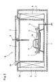
- Fig. 2 shows a state wherein the jig of this embodiment is placed in a high-temperature test unit 5.
- This high-temperature test unit comprises a casing 5a and a lid 5b.
- a heater 6 is incorporated in the side wall of the casing 5a.
- a heat-insulating material 7 is filled outside the heater 6 and in the bottom portion of the casing 5a.
- a temperature measuring element 8 such as a thermocouple is arranged at the central portion of the lid 5b.
- the heat-insulating material 7 is filled around the temperature measuring element 8.
- the semiconductor device storage jig according to this embodiment is placed in the casing 5a.
- a high-temperature of about 350°C is maintained in the high-temperature test unit 5.
- a melting point a of the material of the vessel 1 of the jig, an ambient temperature b , and a melting point c of the conductive member 2 must satisfy the following condition: a > b > c
- the ground terminal 3 for grounding the conductive member 2 is grounded outside the vessel 1.
- the vessel has a rectangular parallelepiped shape.
- the shape of the vessel is not limited to a specific shape if it can contain a conductive member therein.
- a recess may be formed in the inner bottom surface of the vessel to receive and hold the external terminals of the DIP 4 to prevent movement of the DIP 4.
- Fig. 3 shows a semiconductor device storage jig according to the second embodiment of the present invention.
- This storage jig is constituted by integrally forming two insulating plates made of a ceramic material or the like. Two parallel rectangular holes 9a are formed in an upper plate 9. A clamping portion 9b is formed in each hole 9a to clamp external elements 4a of a DIP 4. A metal wiring 11 is formed between the upper plate 9 and a lower plate 10. This metal wiring 11 is located in the bottoms of the two holes 9a and is grounded outside the storage jig. Since the upper ceramic plate 9 and the lower ceramic plate 10 are hermetically bonded to each other, a conductive member 2 does not leak along the metal wiring 11 even if the conductive member 2 is melted.
- Fig. 4 shows a state wherein the DIP 4 is inserted into the upper ceramic plate 9 of the storage jig.
- the external electrodes 4a of the DIP 4 are clamped between the clamping portions 9b.
- the metal wiring 11 is connected at the bottoms of the holes 9a, and the molten conductive member 2 is stored in the holes 9a. Therefore, the external terminals 4a of the DIP 4 are grounded through the molten conductive member 2.
- FIG. 5 shows a semiconductor device storage jig according to the third embodiment of the present invention.
- This storage jig is constituted by a ceramic plate 12. Eight rectangular holes 12a are formed in the upper surface of the ceramic plate 12. A liquid conductive member 2 is filled in each hole 12a. A metal wiring 13 is dipped in the conductive member 2 in these holes 12a. The end portion of the metal wiring 13 is grounded.
- two DIPs 4 are inserted into the four holes 12a, and all the external terminals 4a are properly grounded.
- the DIP is used as a semiconductor device.
- the present invention is not limited to this type of semiconductor device.
- the present invention is also applicable to an IC or LSI of a different type.
- the combination of the materials of the vessel and the conductive member is not limited to the specific one described above. Any combination may be selected if the above condition is satisfied.
- a semiconductor device storage jig As described above, potentials of external terminals of a semiconductor device stored in the vessel can be kept equal to each other. In addition, storage and a test in a high-temperature environment can be performed by properly selecting the material of the vessel.
Landscapes
- Packaging Frangible Articles (AREA)
- Testing Or Measuring Of Semiconductors Or The Like (AREA)
- Container, Conveyance, Adherence, Positioning, Of Wafer (AREA)
- Testing Of Individual Semiconductor Devices (AREA)
- Packaging Of Annular Or Rod-Shaped Articles, Wearing Apparel, Cassettes, Or The Like (AREA)
Applications Claiming Priority (2)
| Application Number | Priority Date | Filing Date | Title |
|---|---|---|---|
| JP39284/90 | 1990-02-20 | ||
| JP2039284A JPH03241851A (ja) | 1990-02-20 | 1990-02-20 | 半導体装置用保存治具 |
Publications (2)
| Publication Number | Publication Date |
|---|---|
| EP0443546A2 true EP0443546A2 (fr) | 1991-08-28 |
| EP0443546A3 EP0443546A3 (en) | 1992-01-15 |
Family
ID=12548860
Family Applications (1)
| Application Number | Title | Priority Date | Filing Date |
|---|---|---|---|
| EP19910102437 Ceased EP0443546A3 (en) | 1990-02-20 | 1991-02-20 | Semiconductor device storage jig |
Country Status (6)
| Country | Link |
|---|---|
| US (1) | US5245276A (fr) |
| EP (1) | EP0443546A3 (fr) |
| JP (1) | JPH03241851A (fr) |
| KR (1) | KR950000100B1 (fr) |
| AU (1) | AU650251B2 (fr) |
| CA (1) | CA2036004A1 (fr) |
Families Citing this family (4)
| Publication number | Priority date | Publication date | Assignee | Title |
|---|---|---|---|---|
| US20060215336A1 (en) * | 2005-03-24 | 2006-09-28 | Honeywell International Inc. | ESD foam ground clip |
| JP2012220404A (ja) * | 2011-04-12 | 2012-11-12 | Sony Computer Entertainment Inc | 電子装置の動作試験装置、動作試験方法、及び電子装置の製造方法 |
| JP7263060B2 (ja) * | 2019-03-11 | 2023-04-24 | 株式会社日本マイクロニクス | 電気的接続装置 |
| KR20230059461A (ko) | 2021-10-26 | 2023-05-03 | 삼성전자주식회사 | 의류처리장치의 세제공급장치 |
Family Cites Families (15)
| Publication number | Priority date | Publication date | Assignee | Title |
|---|---|---|---|---|
| DE2214491A1 (de) * | 1972-03-24 | 1973-10-04 | Sergio Bellan | Hydraulisches hebegeraet |
| US3976916A (en) * | 1975-01-15 | 1976-08-24 | Consan Pacific Incorporated | Antistatic equipment |
| GB1568750A (en) * | 1977-08-03 | 1980-06-04 | Perrens R | Television apparatus |
| US4327832A (en) * | 1980-06-26 | 1982-05-04 | Thielex Plastics Corporation | Container for packaging semiconductor components |
| DE3130324A1 (de) * | 1981-07-31 | 1983-02-17 | GAO Gesellschaft für Automation und Organisation mbH, 8000 München | Traegerelement fuer einen ic-baustein |
| US4472756A (en) * | 1981-09-30 | 1984-09-18 | Senichi Masuda | Duct type charge eliminator |
| US4623951A (en) * | 1982-05-24 | 1986-11-18 | Hughes Aircraft Company | Electrically conductive composite structure |
| US4484243A (en) * | 1982-09-30 | 1984-11-20 | General Electric Company | Protective circuit arrangement for a sheathed heating element |
| US4677520A (en) * | 1985-09-13 | 1987-06-30 | James Price | Static charge protector for integrated circuits |
| JPS62105379A (ja) * | 1985-11-01 | 1987-05-15 | 株式会社日立製作所 | コネクタ装置 |
| US4711350A (en) * | 1986-10-27 | 1987-12-08 | Wei Hsiung Yen | Inspectable antistatic container for packing electrical or electronic devices |
| GB2214491A (en) * | 1988-01-21 | 1989-09-06 | Dowty Electronic Components | Semiconductor product carriers |
| DE3810594A1 (de) * | 1988-03-29 | 1989-10-12 | Heigl Helmuth | Anordnung zum schutz integrierter bauelemente vor beschaedigung durch unkontrollierte elektrostatische entladung in handhabungssystemen |
| US4954878A (en) * | 1989-06-29 | 1990-09-04 | Digital Equipment Corp. | Method of packaging and powering integrated circuit chips and the chip assembly formed thereby |
| US4999023A (en) * | 1989-11-14 | 1991-03-12 | Unisys Corporation | High density low reactance socket |
-
1990
- 1990-02-20 JP JP2039284A patent/JPH03241851A/ja active Pending
-
1991
- 1991-02-08 CA CA002036004A patent/CA2036004A1/fr not_active Abandoned
- 1991-02-12 AU AU71009/91A patent/AU650251B2/en not_active Ceased
- 1991-02-20 KR KR1019910002737A patent/KR950000100B1/ko not_active Expired - Fee Related
- 1991-02-20 EP EP19910102437 patent/EP0443546A3/en not_active Ceased
- 1991-02-20 US US07/657,858 patent/US5245276A/en not_active Expired - Fee Related
Also Published As
| Publication number | Publication date |
|---|---|
| AU650251B2 (en) | 1994-06-16 |
| EP0443546A3 (en) | 1992-01-15 |
| KR950000100B1 (ko) | 1995-01-09 |
| JPH03241851A (ja) | 1991-10-29 |
| KR920000121A (ko) | 1992-01-10 |
| US5245276A (en) | 1993-09-14 |
| AU7100991A (en) | 1991-08-22 |
| CA2036004A1 (fr) | 1991-08-21 |
Similar Documents
| Publication | Publication Date | Title |
|---|---|---|
| EP0239322A2 (fr) | Ensemble à composants refroidis | |
| US4371912A (en) | Method of mounting interrelated components | |
| US5260601A (en) | Edge-mounted, surface-mount package for semiconductor integrated circuit devices | |
| US4766371A (en) | Test board for semiconductor packages | |
| EP0333374A2 (fr) | Empaquetage du type montage en surface, monté en bord, pour dispositifs semi-conducteurs à circuit intégré | |
| KR101445397B1 (ko) | 소켓용 어댑터 장치 | |
| US4992987A (en) | Battery package for integrated circuits | |
| JPS63117443A (ja) | 回路モジュ−ル用のホルダ | |
| EP0098028A2 (fr) | Empaquetage qui peut être scellé hermétiquement pour dispositifs électroniques hybrides à l'état solide et dispositifs similaires | |
| GB2212754A (en) | Electronic componenet chip holder and method of handling electronic component chips | |
| US3550766A (en) | Flat electronic package assembly | |
| US4885662A (en) | Circuit module connection system | |
| US4734820A (en) | Cryogenic packaging scheme | |
| JPH0412624B2 (fr) | ||
| US5245276A (en) | Semiconductor device storage jig | |
| US3909678A (en) | Packaging structure for a plurality of wafer type integrated circuit elements | |
| US4272140A (en) | Arrangement for mounting dual-in-line packaged integrated circuits to thick/thin film circuits | |
| US3447040A (en) | Micro-element carrier-connector | |
| EP0095391B1 (fr) | Montage de supports sans conducteur pour puces | |
| US3105868A (en) | Circuit packaging module | |
| US3278018A (en) | Handling miniature solid-state devices | |
| EP0145327A2 (fr) | Arrangement d'interface électrique | |
| US2935722A (en) | Electrical socket connector with mercury contact | |
| US4767983A (en) | Test fixture for electronic device packages | |
| EP0505193B1 (fr) | Couvercle pour empaquetage de composants électriques |
Legal Events
| Date | Code | Title | Description |
|---|---|---|---|
| PUAI | Public reference made under article 153(3) epc to a published international application that has entered the european phase |
Free format text: ORIGINAL CODE: 0009012 |
|
| AK | Designated contracting states |
Kind code of ref document: A2 Designated state(s): DE FR GB IT NL |
|
| PUAL | Search report despatched |
Free format text: ORIGINAL CODE: 0009013 |
|
| AK | Designated contracting states |
Kind code of ref document: A3 Designated state(s): DE FR GB IT NL |
|
| 17P | Request for examination filed |
Effective date: 19920311 |
|
| 17Q | First examination report despatched |
Effective date: 19921116 |
|
| GRAG | Despatch of communication of intention to grant |
Free format text: ORIGINAL CODE: EPIDOS AGRA |
|
| STAA | Information on the status of an ep patent application or granted ep patent |
Free format text: STATUS: THE APPLICATION HAS BEEN REFUSED |
|
| 18R | Application refused |
Effective date: 19970504 |