EP0443921A1 - Verarbeitungsverfahren von digitalen Kontrolldaten, die mit einem HD-MAC-Videosignal verbunden sind - Google Patents
Verarbeitungsverfahren von digitalen Kontrolldaten, die mit einem HD-MAC-Videosignal verbunden sind Download PDFInfo
- Publication number
- EP0443921A1 EP0443921A1 EP91400396A EP91400396A EP0443921A1 EP 0443921 A1 EP0443921 A1 EP 0443921A1 EP 91400396 A EP91400396 A EP 91400396A EP 91400396 A EP91400396 A EP 91400396A EP 0443921 A1 EP0443921 A1 EP 0443921A1
- Authority
- EP
- European Patent Office
- Prior art keywords
- data
- digital control
- control data
- processing
- circuit
- Prior art date
- Legal status (The legal status is an assumption and is not a legal conclusion. Google has not performed a legal analysis and makes no representation as to the accuracy of the status listed.)
- Granted
Links
Images

Classifications
-
- H—ELECTRICITY
- H04—ELECTRIC COMMUNICATION TECHNIQUE
- H04N—PICTORIAL COMMUNICATION, e.g. TELEVISION
- H04N7/00—Television systems
- H04N7/08—Systems for the simultaneous or sequential transmission of more than one television signal, e.g. additional information signals, the signals occupying wholly or partially the same frequency band, e.g. by time division
- H04N7/083—Systems for the simultaneous or sequential transmission of more than one television signal, e.g. additional information signals, the signals occupying wholly or partially the same frequency band, e.g. by time division with signal insertion during the vertical and the horizontal blanking interval, e.g. MAC data signals
-
- H—ELECTRICITY
- H04—ELECTRIC COMMUNICATION TECHNIQUE
- H04N—PICTORIAL COMMUNICATION, e.g. TELEVISION
- H04N7/00—Television systems
- H04N7/015—High-definition television systems
- H04N7/0152—High-definition television systems using spatial or temporal subsampling
- H04N7/0155—High-definition television systems using spatial or temporal subsampling using pixel blocks
- H04N7/0157—High-definition television systems using spatial or temporal subsampling using pixel blocks with motion estimation, e.g. involving the use of motion vectors
Definitions
- the present invention relates to a method for processing digital control data associated with a video signal of the HD-MAC type as well as a device for implementing this method.
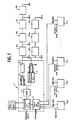
- the DATV data associated with an HD-MAC type video signal are therefore decoded in a decoding system as shown in FIG. 1.
- the digital assistance data includes more particularly data indicating the transmission mode used or branch decision data referenced "BD" and vector-movement data referenced "MV”. All of these data are coded on 11 bits and they relate to an image block.
- the decoding device comprises two memories referenced RAM1, RAM2, each memory being capable of storing the DATV data corresponding to a processing period, namely to an even image and an odd image. For the case considered above, each memory has a capacity of at least 6480 words of 11 bits. As shown in FIG.
- the decoder 1 comprises a circuit for controlling the memories RAM1 and RAM2 which receives the DATV data as an input and which manages the operation of the memories RAM1 and RAM2 in reading and writing as will be described below.
- the decoder 1 also includes a time base 3 which is connected to the control circuit 2 and receives a control signal. The time base transmits various synchronization signals referenced respectively SYNCHRO O, SYNCHRO 1, SYNCHRO 2, ..., SYNCHRO X to processing circuits external to the decoder.
- the decoder 1 comprises a ROM (Read only memory in English) 4 memory in which is stored a decoding table.
- This memory 4 is connected at the output of the control circuit 2.
- a multiplexer 5 which receives as input the branch decision data BD contained in the DATV data. It receives respectively odd image BD branch decision data referenced BD-OFR and even image branch image decision data referenced BD-EFR and it outputs decoded branch decision information which is sent on a circuit to delay 6 compensating for the delay due to the processing of other DATV data as will be explained in detail below. There is therefore obtained at the output of circuit 6 non-delayed branch decision information referenced BDO.
- the output of the memory ROM4 is connected to a circuit for processing the address of the vector-movement data MV.
- This circuit gives as output the vector-movement data corresponding to the even image and referenced MV-EFR and the vector-movement data corresponding to the odd image and referenced MV-OFR. These data are multiplexed in the multiplexer 8 so as to obtain at the output the non-delayed vector-movement data MVO.
- the DATV data coded over a processing period corresponding to an even image and an odd image, ie 80 ms are transmitted 80 ms before the corresponding video signal. This explains the use of two memories RAM1 and RAM2 which are used alternately in read mode and in write mode.
- the DATV data of the following processing period are stored in the memory RAM2 which operates in write mode.
- this decoding device one therefore obtains at the output of the decoder the branch decision data decoded BDO on two bits, and the vector-motion data decoded MVO on 8 bits.
- this BDO and MVO data must be delayed, because the video signal processing circuit called bandwidth reduction decoder also uses the BD4, BD2, BD1 data which are delayed by 20ms, 60ms, 80ms respectively with respect to BDO and MV2 data which is delayed by 60 ms compared to MVO to carry out the proper processing of the video signal according to the compression mode used.
- this delay is accomplished using delay circuits such as frame memories which can provide delays of 20ms or more. These memories are referenced 9a, 9b, 9c, 9d and 10a, 10b, 10c in FIG. 1. Consequently, at the output of the memory 9a, the branch decision data BD4 is obtained, at the output of the memory 9c we obtain the branch decision data BD2 and at the output of the memory 9d we obtain the branch decision data BD1, while at the output of the circuit 10c we obtain the vector-movement data MV2.
- delay circuits such as frame memories which can provide delays of 20ms or more.
- the decoder 1 in addition to the digital assistance data BDX and MVX, the decoder 1 must also generate several versions offset in time of the synchronization signals.
- These synchronization signals may in particular include line-synchronization, line-parity, frame-parity, image-parity information.
- These synchronization signals with their specific delay must be connected to different circuits in the video signal processing device.
- the delays can vary from a few clock cycles (37ns) to several line periods (32 ⁇ s). Consequently, as shown in FIG. 1, the transmission of all these signals in parallel requires a large number of interconnections on the printed circuit.
- the delay circuits are produced using additional integrated circuits, which entails a high cost for producing the entire decoding device.
- the present invention therefore aims to remedy this drawback by proposing a new method for processing the digital control data associated with a video signal of the HD-MAC type as well as a new device for implementing this method.
- the subject of the present invention is a method for processing the digital control data associated with an HD-MAC type video signal in which, over a processing period, the digital data of control associated with the video signal of the next processing period, characterized in that the digital control data corresponding to n successive processing periods (n ⁇ 2) are stored and then the data thus decoded, stored so as to output the desired digital control data in parallel with their specific delay.
- the processing period corresponds to the transmission period of two images, even and odd respectively.
- the storage of digital control data is carried out in n + 1 memories managed by circular permutation, one of the memories being in write mode while the other memories are in read mode.
- the digital control data obtained at the output of the decoder as well as the synchronization data are transmitted to processing circuits via at least one serial bus comprising two signal signal lines. a bit. This makes it possible to reduce the number of outputs provided on the printed circuit for producing the decoding device.
- the synchronization information as well as the digital assistance data are successively sent to the processing circuits which need it with their own delay, said circuits themselves generating the delay of the synchronization signals.
- the present invention also relates to a device for implementing the above method.
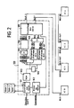
- this device comprises three memories capable of each storing the digital control data relating to a processing period, a circuit for controlling the memories receiving the digital control data (DATV) and managing the memories by circular permutation, a time base linked to the circuit control and generating synchronization signals, a decoding table connected at the output of the control circuit, a locking circuit connected at the output of the decoding table, a first address processing (MV) circuit connected at the output of the decoding table and delivering in parallel the vector-movement data (MV) of an even image and an odd image corresponding to a first processing period, a second address processing circuit (MV) connected at the output of the circuit for locking and delivering in parallel the vector-motion (MV) data of an even image and an odd image corresponding to a second processing period, a multiplexer receiving vector-motion (MV) data from the two processing circuits address and delivering the MVO and MV2 data in parallel, a multiplexer receiving the input of the decoding table and the locking circuit respectively the decision data branch
- the above device further comprises a serial bus formatting circuit receiving as input the decoded digital control data BD0 BD1, BD2, BD4 and MVO, MV2 as well as the synchronization information and sending them by serial on at least one bus consisting of two one-bit signal lines.
- this decoding device comprises three memories RAM1, RAM2, RAM3 intended to store the digital control information corresponding to two periods of 80 ms.
- each memory RAM1, RAM2 or RAM3 has a capacity of at least 6480 words of 11 bits.
- the storage of digital DATV control data corresponding to two 80 ms periods makes it possible to obtain in parallel the decoded digital control information BD0, BD1, BD2, BD4, and MVO, MV2 as will be explained in more detail below.
- the decoder 100 itself comprises a circuit 101 for controlling the RAM memories substantially identical to the circuit for controlling the RAM memories of the decoder in FIG. 1.
- This circuit for controlling the RAM memories receives the DATV data as input and manages memories RAM1, RAM2, RAM3 by circular permutation.
- the circuit 101 for controlling the RAM memories is connected to a time base 102 which receives control or clock signals and sends synchronization signals to different circuits.
- the decoder 100 includes a decoding table stored in a ROM memory 103. This memory 103 is connected at the output of the circuit 101 for controlling the RAM memories.
- the memory 103 is connected to a latching circuit 104.
- the decoder 100 further comprises a first multiplexer 105 which receives at the input of branch decision data even and odd images (BD-EFR * and BD-OFR *) from the locking circuit 104 as well as the data of branch decision of the even and odd images (BD-EFR and BD-OFR) coming directly from the decoding table 103.
- the output of the multiplexer 105 is sent on a delay circuit 106 compensating for the delays resulting from the processing of other data and outputs the branch decision data with the desired specific delays BD0, BD1, BD2, BD4.
- the decoder 100 comprises two vector-motion address processing circuits MV 107 and 107 ′.
- the circuit 107 is connected directly at the output of the decoding table 103 while the circuit 107 ′ is connected at the output of the locking circuit 104.
- These processing circuits 107 and 107 ′ give as output the vector-motion data corresponding to the even images and odd of the first processing period referenced MV-EFR * and MV-OFR * for circuit 107 ′ and the vector-motion data corresponding to the even and odd images of the second processing period referenced MV-EFR and MV-OFR for the processing circuit 107.
- the vector-movement data MV-OFR *, MV-EFR *, MV-OFR, MV-EFR are sent as input to a multiplexer 108 giving as output the vector-movement data MV0 and MV2.
- all of the digital control data with their specific delay BD0, BD1, BD2, BD4, MV0, MV2 as well as the synchronization information originating from the time base 102 are sent to a circuit 109 for formatting a serial bus which makes it possible to send on two serial buses BUS 1 and BUS 2 each consisting of two one-bit signal lines, the digital control data necessary to different circuits for processing the video signal referenced respectively IC0, IC1, 1C2, ..., ICX.
- the information transmitted by the serial bus BUS 1 is sent to the processing circuit IC0.
- the serial bus BUS 1 transmits only the digital control data BD0 and MV0 to the circuit IC0.
- the signal line S1 is used for the transmission of digital control data BD1, BD2, BD4 and signals coded on 8 bits.
- the transmission sequence on the basis of a 32 ⁇ s HDTV line can be, by way of illustration, that shown in FIG. 4.
- the first word transmitted on line S1 is a word FF.
- the word FF is a specific word which means that the next word is a synchronization word. It can be coded as 11111111.
- the second word transmitted on S1 is the word SYC1 which is a synchronization word.
- This word comprises a first bit set to "0" followed by 7 bits giving information, in particular on the start of a line, the end of a line and the parity of an image as shown in FIG. 4.
- the line S1 will be transmitted 90 successive words containing the BD decision data relating to an image, each word BD comprising the data BD1, BD2, BD4 and starting with a bit "0".
- a second word FF is transmitted, then a synchronization word SYC2 providing in particular end of line information.
- the data relating to the motion vector MV2 is transmitted in the form of 8-bit words in phase with the data BD.
- the word MV contains information on the horizontal components MVH and the vertical components MVV of a vector-motion word MV.
- the serial bus BUS 2 is connected at the input of circuit IC1 to the input referenced BUS-IN, then the information sent on the serial bus BUS 2 propagates through the other circuits IC2, ... , ICX by being connected between the BUS-OUT outputs and the BUS-IN inputs of these circuits. Therefore, each circuit is responsible for the output from the serial bus and transmits the data circulating on the serial bus BUS 2 to the next circuit with its own delay corresponding to its own delay. Thus, the DATV data supplied by the serial bus is always in phase with the video data.
- this serial bus for the transmission of decoded DATV digital control data significantly reduces the number of outputs on the DATV 100 decoder as well as the number of interconnections on the printed circuit.
- the propagation of the serial bus from one circuit to another in phase with the video data also simplifies the interface design between the DATV decoder and all the other circuits, as shown in FIG. 2.
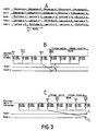
- FIGS. 3B and 3C show an example of decoded DATV data making it possible to obtain all of the desired digital control data with their specific delay.
- This sequence 2 corresponds to an even image and to an odd image and has a duration of 80 ms.
- the memory RAM1 contains the 6480 coded words corresponding to the digital control data of the sequence 2.
- the cycle T1 represented in FIG. 3B corresponds to the cycle for reading word 1 in the memory RAM1.
- the decoding of this word provides the digital BD decision control data and of vector-motion MV relating to the sequence 2.
- the memory RAM2 contains the 6480 coded words of the digital control data DATV relating to the sequence 1
- This cycle referenced T2 represents the reading cycle of word 1 in the memory RAM2.
- the decoding of this word provides the digital control data relating to the sequence 1.
- BD0 BD-EFR
- BD1 BD-EFR *
- BD2 BD-EFR *
- BD4 BD-OFR *
- MVO MV-EFR
- MV2 MV -EFR *.
- the cycle T'1 represents the reading cycle of the 6480 th word in the RAM1 memory.
- the decoding of this word provides the data BD and MV relating to the sequence 2.
- the cycle T'2 represents the reading cycle of the 6480 th word in the RAM2.
- the decoding of this word provides digital control data BD and MV relating to the sequence 1.
- BD0 BD-OFR
- BD1 BD-OFR *
- BD2 BD-EFR
- BD4 BD-OFR
- MV0 MV-OFR
- MV2 MV-EFR.
- the use of the decoder therefore makes it possible to eliminate the delay circuits such as the 20 ms frame memories used in the decoding circuit of the prior art. These circuits are replaced by a single RAM2 memory of 6480 words of 11 bits which significantly reduces the cost of the circuit.
Landscapes
- Engineering & Computer Science (AREA)
- Multimedia (AREA)
- Signal Processing (AREA)
- Power Engineering (AREA)
- Compression Or Coding Systems Of Tv Signals (AREA)
- Television Systems (AREA)
Applications Claiming Priority (2)
| Application Number | Priority Date | Filing Date | Title |
|---|---|---|---|
| FR9002259A FR2658971B1 (fr) | 1990-02-23 | 1990-02-23 | Procede de traitement des donnees numeriques de controle associees a un signal video de type hd-mac et dispositif pour la mise en óoeuvre du procede. |
| FR9002259 | 1990-02-23 |
Publications (2)
| Publication Number | Publication Date |
|---|---|
| EP0443921A1 true EP0443921A1 (de) | 1991-08-28 |
| EP0443921B1 EP0443921B1 (de) | 1995-09-13 |
Family
ID=9394067
Family Applications (1)
| Application Number | Title | Priority Date | Filing Date |
|---|---|---|---|
| EP91400396A Expired - Lifetime EP0443921B1 (de) | 1990-02-23 | 1991-02-15 | Verarbeitungsverfahren von digitalen Kontrolldaten, die mit einem HD-MAC-Videosignal verbunden sind |
Country Status (6)
| Country | Link |
|---|---|
| US (1) | US5191418A (de) |
| EP (1) | EP0443921B1 (de) |
| JP (1) | JPH04216284A (de) |
| DE (1) | DE69112865T2 (de) |
| ES (1) | ES2079592T3 (de) |
| FR (1) | FR2658971B1 (de) |
Cited By (1)
| Publication number | Priority date | Publication date | Assignee | Title |
|---|---|---|---|---|
| FR2684257A1 (fr) * | 1991-11-27 | 1993-05-28 | Thomson Consumer Electronics | Dispositif de decodage d'informations de mouvement en television haute definition. |
Families Citing this family (16)
| Publication number | Priority date | Publication date | Assignee | Title |
|---|---|---|---|---|
| US5828786A (en) * | 1993-12-02 | 1998-10-27 | General Instrument Corporation | Analyzer and methods for detecting and processing video data types in a video data stream |
| KR0140506B1 (ko) * | 1993-12-29 | 1998-06-15 | 김주용 | 완전 디지탈 방식의 고화질 텔레비젼에서의 분배기 설계 |
| US6631435B1 (en) * | 1996-02-02 | 2003-10-07 | Sony Corporation | Application programming interface for data transfer and bus management over a bus structure |
| US7577782B2 (en) | 1996-02-02 | 2009-08-18 | Sony Corporation | Application programming interface for data transfer and bus management over a bus structure |
| US6233637B1 (en) * | 1996-03-07 | 2001-05-15 | Sony Corporation | Isochronous data pipe for managing and manipulating a high-speed stream of isochronous data flowing between an application and a bus structure |
| US6519268B1 (en) | 1996-03-07 | 2003-02-11 | Sony Corporation | Asynchronous data pipe for automatically managing asynchronous data transfers between an application and a bus structure |
| US6167471A (en) | 1998-10-14 | 2000-12-26 | Sony Corporation | Method of and apparatus for dispatching a processing element to a program location based on channel number of received data |
| US6263023B1 (en) | 1998-10-15 | 2001-07-17 | International Business Machines Corporation | High definition television decoder |
| US6859846B2 (en) * | 1999-05-12 | 2005-02-22 | Sony Corporation | Method of distributed recording whereby the need to transition to a second recording device from a first recording device is broadcast by the first recording device |
| US6247069B1 (en) | 1999-05-12 | 2001-06-12 | Sony Corporation | Automatically configuring storage array including a plurality of media storage devices for storing and providing data within a network of devices |
| US6721859B1 (en) | 1999-10-21 | 2004-04-13 | Sony Corporation | Multi-protocol media storage device implementing protocols optimized for storing and retrieving both asynchronous and isochronous data |
| US6523108B1 (en) | 1999-11-23 | 2003-02-18 | Sony Corporation | Method of and apparatus for extracting a string of bits from a binary bit string and depositing a string of bits onto a binary bit string |
| US7720821B1 (en) | 2000-06-30 | 2010-05-18 | Sony Corporation | Method of and apparatus for writing and reading time sensitive data within a storage device |
| US6904475B1 (en) | 2000-11-06 | 2005-06-07 | Sony Corporation | Programmable first-in first-out (FIFO) memory buffer for concurrent data stream handling |
| US7124292B2 (en) * | 2001-05-21 | 2006-10-17 | Sony Corporation | Automatically configuring storage array including a plurality of media storage devices for storing and providing data within a network of devices |
| US7430201B1 (en) * | 2003-03-21 | 2008-09-30 | Transwitch Corporation | Methods and apparatus for accessing full bandwidth in an asynchronous data transfer and source traffic control system |
Citations (4)
| Publication number | Priority date | Publication date | Assignee | Title |
|---|---|---|---|---|
| US4789860A (en) * | 1985-03-12 | 1988-12-06 | U.S. Philips Corp. | Interface between a receiver and a sub-system |
| EP0342756A1 (de) * | 1988-05-20 | 1989-11-23 | Laboratoires D'electronique Philips | Fernsehsende- und Empfangssystem mit hoher Auflösung und verminderter Datenrate |
| EP0349454A1 (de) * | 1988-06-24 | 1990-01-03 | France Telecom | Verfahren zur Kodierung von Hilfsdaten für die Rekonstruktion eines unterabgetasteten, elektronischen Bildes |
| EP0386805A2 (de) * | 1989-01-11 | 1990-09-12 | Philips Electronics Uk Limited | Verarbeitung von Fernsehsignalen mit einer hohen Auflösung |
Family Cites Families (4)
| Publication number | Priority date | Publication date | Assignee | Title |
|---|---|---|---|---|
| US4794447A (en) * | 1986-11-17 | 1988-12-27 | North American Philips Corporation | Method and apparatus for transmitting and receiving a high definition NTSC compatible television signal over a single DBS channel in time division multiplex form |
| GB2201315B (en) * | 1987-02-20 | 1991-02-13 | Philips Electronic Associated | Television transmission system |
| EP0322956B1 (de) * | 1987-12-22 | 1994-08-03 | Koninklijke Philips Electronics N.V. | Videosignalkodierung und -dekodierung mit einem adaptiven Filter |
| US5029000A (en) * | 1988-12-23 | 1991-07-02 | U.S. Philips Corp. | High definition television system |
-
1990
- 1990-02-23 FR FR9002259A patent/FR2658971B1/fr not_active Expired - Fee Related
-
1991
- 1991-02-15 EP EP91400396A patent/EP0443921B1/de not_active Expired - Lifetime
- 1991-02-15 ES ES91400396T patent/ES2079592T3/es not_active Expired - Lifetime
- 1991-02-15 DE DE69112865T patent/DE69112865T2/de not_active Expired - Fee Related
- 1991-02-20 US US07/658,335 patent/US5191418A/en not_active Expired - Fee Related
- 1991-02-25 JP JP3050156A patent/JPH04216284A/ja not_active Withdrawn
Patent Citations (4)
| Publication number | Priority date | Publication date | Assignee | Title |
|---|---|---|---|---|
| US4789860A (en) * | 1985-03-12 | 1988-12-06 | U.S. Philips Corp. | Interface between a receiver and a sub-system |
| EP0342756A1 (de) * | 1988-05-20 | 1989-11-23 | Laboratoires D'electronique Philips | Fernsehsende- und Empfangssystem mit hoher Auflösung und verminderter Datenrate |
| EP0349454A1 (de) * | 1988-06-24 | 1990-01-03 | France Telecom | Verfahren zur Kodierung von Hilfsdaten für die Rekonstruktion eines unterabgetasteten, elektronischen Bildes |
| EP0386805A2 (de) * | 1989-01-11 | 1990-09-12 | Philips Electronics Uk Limited | Verarbeitung von Fernsehsignalen mit einer hohen Auflösung |
Cited By (2)
| Publication number | Priority date | Publication date | Assignee | Title |
|---|---|---|---|---|
| FR2684257A1 (fr) * | 1991-11-27 | 1993-05-28 | Thomson Consumer Electronics | Dispositif de decodage d'informations de mouvement en television haute definition. |
| WO1993011634A1 (fr) * | 1991-11-27 | 1993-06-10 | Thomson Consumer Electronics S.A. | Dispositif de decodage d'informations de mouvement en television haute definition |
Also Published As
| Publication number | Publication date |
|---|---|
| FR2658971B1 (fr) | 1995-07-28 |
| DE69112865D1 (de) | 1995-10-19 |
| FR2658971A1 (fr) | 1991-08-30 |
| ES2079592T3 (es) | 1996-01-16 |
| EP0443921B1 (de) | 1995-09-13 |
| US5191418A (en) | 1993-03-02 |
| JPH04216284A (ja) | 1992-08-06 |
| DE69112865T2 (de) | 1996-03-21 |
Similar Documents
| Publication | Publication Date | Title |
|---|---|---|
| EP0443921B1 (de) | Verarbeitungsverfahren von digitalen Kontrolldaten, die mit einem HD-MAC-Videosignal verbunden sind | |
| FR2461405A1 (fr) | Systeme de codage et de decodage d'un signal visiophonique numerique | |
| FR2466837A1 (fr) | Memoire tampon d'interface terrestre a acces multiples par repartition de temps pour operations entrelacees | |
| EP0418952B1 (de) | Vorrichtung zum Codieren von zweidimensionalen Informationen und entsprechende Decodiervorrichtung | |
| EP0368400B1 (de) | Kodierung, Dekodierung und Übertragungssystem für Fernsehbilder | |
| FR2549258A1 (fr) | Procede de commande pour transfert de donnees | |
| FR2535561A1 (fr) | Systeme de traitement de signaux video | |
| FR2650718A1 (fr) | Dispositif de transformation d'une information de mouvement en un signal de detection de mouvement a la frequence trame et au nombre de lignes souhaites pour un recepteur de television haute definition | |
| FR2589302A1 (fr) | Systeme de thermographie infrarouge a sensibilite amelioree par accumulation progressive des lignes de l'image | |
| WO1989010039A1 (fr) | Dispositif de decodage et systeme de transmission d'images de television a haute definition | |
| EP0404238B1 (de) | Signalverarbeitungseinrichtungen vor und nach Übertragung und/oder Speicherung mit Datenflussverminderung, und Verfahren zur Übertragung und/oder Speicherung von Signalen mit solchen Einrichtungen | |
| FR3020543A1 (fr) | Procede de gestion de la communication entre deux dispositifs mutuellement connectes par un lien serie, par exemple un protocole d'interface serie point a point | |
| FR2638310A1 (fr) | Procede et dispositif de conversion du rythme temporel d'images de television a haute definition, et decodeur d'images de television comprenant un tel dispositif | |
| EP0063990A1 (de) | Verfahren zur Bildübertragung mit beschränktem Datafluss; Übertragungssystem zur Durchführung dieses Verfahrens | |
| EP0690623A1 (de) | Verfahren und Einrichtung zur Einfügung von asynchronen Daten in ein digitales Signal | |
| FR2790322A1 (fr) | Recepteur, circuit programmable et procede de calcul de filtres numeriques | |
| EP0552099B1 (de) | Mehrkomponenten X-Paketkodierer und Dekodierer dafür | |
| EP0424269A1 (de) | Gerät zur Bewegungskompensation und Fernsehempfänger mit einem solchen Gerät | |
| EP0675651A1 (de) | Verfahren und Vorrichtung zur Wiedergabe einer entfernten Quelle empfangenen digitalen Bildfolge | |
| EP0452477A1 (de) | Verfahren zum formatieren von kontrollinformationen eines digitalisierten videosignals auf einen digitalen bus | |
| CN116886961B (zh) | 一种分布式直播视频插帧方法、设备、系统及存储介质 | |
| EP0089731B1 (de) | Verfahren zum Übersenden von Daten in einem Fernsehempfänger und Empfänger, der das Verfahren verwendet | |
| US5327239A (en) | Video data splitting circuit | |
| FR2556902A1 (fr) | Procede et dispositif de filtrage de rang determine d'un signal numerique et application au filtrage median bidimensionnel separable | |
| EP0321357A1 (de) | Verfahren zur Unterabtastung einer Folge von elektronischen Bildern in der Achse der Bewegung |
Legal Events
| Date | Code | Title | Description |
|---|---|---|---|
| PUAI | Public reference made under article 153(3) epc to a published international application that has entered the european phase |
Free format text: ORIGINAL CODE: 0009012 |
|
| AK | Designated contracting states |
Kind code of ref document: A1 Designated state(s): DE ES GB IT NL SE |
|
| 17P | Request for examination filed |
Effective date: 19910912 |
|
| 17Q | First examination report despatched |
Effective date: 19940225 |
|
| GRAA | (expected) grant |
Free format text: ORIGINAL CODE: 0009210 |
|
| AK | Designated contracting states |
Kind code of ref document: B1 Designated state(s): DE ES GB IT NL SE |
|
| PG25 | Lapsed in a contracting state [announced via postgrant information from national office to epo] |
Ref country code: NL Free format text: LAPSE BECAUSE OF FAILURE TO SUBMIT A TRANSLATION OF THE DESCRIPTION OR TO PAY THE FEE WITHIN THE PRESCRIBED TIME-LIMIT Effective date: 19950913 |
|
| REF | Corresponds to: |
Ref document number: 69112865 Country of ref document: DE Date of ref document: 19951019 |
|
| ITF | It: translation for a ep patent filed | ||
| GBT | Gb: translation of ep patent filed (gb section 77(6)(a)/1977) |
Effective date: 19951110 |
|
| PG25 | Lapsed in a contracting state [announced via postgrant information from national office to epo] |
Ref country code: SE Effective date: 19951213 |
|
| REG | Reference to a national code |
Ref country code: ES Ref legal event code: FG2A Ref document number: 2079592 Country of ref document: ES Kind code of ref document: T3 |
|
| NLV1 | Nl: lapsed or annulled due to failure to fulfill the requirements of art. 29p and 29m of the patents act | ||
| PLBE | No opposition filed within time limit |
Free format text: ORIGINAL CODE: 0009261 |
|
| STAA | Information on the status of an ep patent application or granted ep patent |
Free format text: STATUS: NO OPPOSITION FILED WITHIN TIME LIMIT |
|
| 26N | No opposition filed | ||
| PGFP | Annual fee paid to national office [announced via postgrant information from national office to epo] |
Ref country code: DE Payment date: 19970421 Year of fee payment: 7 |
|
| PGFP | Annual fee paid to national office [announced via postgrant information from national office to epo] |
Ref country code: GB Payment date: 19980116 Year of fee payment: 8 |
|
| PGFP | Annual fee paid to national office [announced via postgrant information from national office to epo] |
Ref country code: ES Payment date: 19980227 Year of fee payment: 8 |
|
| PG25 | Lapsed in a contracting state [announced via postgrant information from national office to epo] |
Ref country code: DE Free format text: LAPSE BECAUSE OF NON-PAYMENT OF DUE FEES Effective date: 19981103 |
|
| PG25 | Lapsed in a contracting state [announced via postgrant information from national office to epo] |
Ref country code: GB Free format text: LAPSE BECAUSE OF NON-PAYMENT OF DUE FEES Effective date: 19990215 |
|
| PG25 | Lapsed in a contracting state [announced via postgrant information from national office to epo] |
Ref country code: ES Free format text: THE PATENT HAS BEEN ANNULLED BY A DECISION OF A NATIONAL AUTHORITY Effective date: 19990216 |
|
| GBPC | Gb: european patent ceased through non-payment of renewal fee |
Effective date: 19990215 |
|
| REG | Reference to a national code |
Ref country code: ES Ref legal event code: FD2A Effective date: 20010604 |
|
| PG25 | Lapsed in a contracting state [announced via postgrant information from national office to epo] |
Ref country code: IT Free format text: LAPSE BECAUSE OF NON-PAYMENT OF DUE FEES;WARNING: LAPSES OF ITALIAN PATENTS WITH EFFECTIVE DATE BEFORE 2007 MAY HAVE OCCURRED AT ANY TIME BEFORE 2007. THE CORRECT EFFECTIVE DATE MAY BE DIFFERENT FROM THE ONE RECORDED. Effective date: 20050215 |