EP0444211A1 - Druckplatte unter verwendung eines ladungshaltenden mediums, verfahren zu deren herstellung und ablösesystem, das ein ladungshaltendes medium verwendet - Google Patents
Druckplatte unter verwendung eines ladungshaltenden mediums, verfahren zu deren herstellung und ablösesystem, das ein ladungshaltendes medium verwendet Download PDFInfo
- Publication number
- EP0444211A1 EP0444211A1 EP90913869A EP90913869A EP0444211A1 EP 0444211 A1 EP0444211 A1 EP 0444211A1 EP 90913869 A EP90913869 A EP 90913869A EP 90913869 A EP90913869 A EP 90913869A EP 0444211 A1 EP0444211 A1 EP 0444211A1
- Authority
- EP
- European Patent Office
- Prior art keywords
- charge carrier
- layer
- charge
- toner
- carrier medium
- Prior art date
- Legal status (The legal status is an assumption and is not a legal conclusion. Google has not performed a legal analysis and makes no representation as to the accuracy of the status listed.)
- Withdrawn
Links
Images






Classifications
-
- G—PHYSICS
- G03—PHOTOGRAPHY; CINEMATOGRAPHY; ANALOGOUS TECHNIQUES USING WAVES OTHER THAN OPTICAL WAVES; ELECTROGRAPHY; HOLOGRAPHY
- G03G—ELECTROGRAPHY; ELECTROPHOTOGRAPHY; MAGNETOGRAPHY
- G03G13/00—Electrographic processes using a charge pattern
- G03G13/26—Electrographic processes using a charge pattern for the production of printing plates for non-xerographic printing processes
-
- G—PHYSICS
- G03—PHOTOGRAPHY; CINEMATOGRAPHY; ANALOGOUS TECHNIQUES USING WAVES OTHER THAN OPTICAL WAVES; ELECTROGRAPHY; HOLOGRAPHY
- G03G—ELECTROGRAPHY; ELECTROPHOTOGRAPHY; MAGNETOGRAPHY
- G03G13/00—Electrographic processes using a charge pattern
- G03G13/26—Electrographic processes using a charge pattern for the production of printing plates for non-xerographic printing processes
- G03G13/28—Planographic printing plates
-
- G—PHYSICS
- G03—PHOTOGRAPHY; CINEMATOGRAPHY; ANALOGOUS TECHNIQUES USING WAVES OTHER THAN OPTICAL WAVES; ELECTROGRAPHY; HOLOGRAPHY
- G03G—ELECTROGRAPHY; ELECTROPHOTOGRAPHY; MAGNETOGRAPHY
- G03G5/00—Recording-members for original recording by exposure, e.g. to light, to heat or to electrons; Manufacture thereof; Selection of materials therefor
- G03G5/02—Charge-receiving layers
Definitions
- the present invention relates to a printing plate formed of charge carrier media, a process for making printing plates with charge carrier media and a page make-up system making use of charge carrier media, which is designed to make up pages by forming electrostatic latent images of the original images directly on given positions on printing plates formed of charge carrier media and at given magnifications.
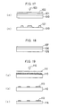
- the plate-making system shown in Fig. 17 is generally implemented as follows.
- an aluminium plate 100 is provided, which has been polished by such polishing techniques as ball or brush polishing or "grained" in the jargon of the field, and a photosensitive resin layer 101 is formed on this aluminium plate 100 to form a printing substrate.
- a plate-making film is located in opposition to the resin layer 101, followed by pattern exposure (Fig. 17a) with ultraviolet rays 103, development and drying. In this way, a printing plate including a printing area formed of the resin layer 101 is produced, as shown in Fig. 17b.
- PS presensitized
- wipe-on plates are less costly and more sensitive than the PS plates, but are inferior in serviceability to the PS plates due to some coating steps being needed. Serious limitation is imposed on the operation of the wipe-on plates as well, because so short are they in pot-life or a time span from their being coated to their use, that they must be exposed to light just after the formation of photosensitive layers thereon.
- the PS plates are now virtually supplanting the wipe-on plates.
- the PS plates can serve well, but the sensitivity of their photosensitive layers is not good enough, because they should stand up to long-term storage with the photosensitive layers coated on them.
- the higher the sensitivity of the PS plates the more are they reactive with respect to heat, thus often resulting in their fogging due to thermal reactions during storage. This makes it very difficult to increase the sensitivity of the PS plates.
- a printing substrate obtained by forming a photosensitive resin layer 106 on a grained aluminium plate 105 and forming thereon a layer 107 comprising a silver emulsion.
- This substrate may be processed into a printing plate by similar pattern exposure, development and drying as described in connection with Fig. 17.
- This printing plate has been developed with a view of making up for the defect - low sensitivity - of the PS plates. More exactly, a silver emulsion layer is formed on a PS plate, which is in turn subjected to primary, low-energy exposure, while making use of the high sensitivity of the silver emulsion, thereby developing the silver emulsion. Then, the resulting blackened silver particle pattern is used as the original for allover uniform exposure (secondary exposure) and then development, thereby obtaining a printing plate.
- the objective is to take advantage of such low-energy exposure as laser-scanning exposure or projecting exposure.
- Laser-scanning exposure of printing plates is a technique of vital importance especially when printing is to be carried out in printing plants located at remote places with information fed through communications lines, as is the case with preparing printing plates for "The Wall Street Journal".
- Projecting exposure enables printing plates to be immediately prepared, if only reflection copies are available, and so can dispense with such timeconsuming steps of making film copies through process cameras as required conventionally.
- the plate-making process as shown in Fig. 19 resorts to one electrophotographic technique, wherein a photosensitive material 110 comprising a photoconductive material is first electrostatically charged by corona discharge in a uniform manner, then pattern exposed to light 112 having a given wavelength through a film 111 (Fig. 19a), and finally coated with a toner 113 (Fig. 19b), whereby the toner 113 is deposited onto only a portion of the material 110 that has not been exposed to the light 112. After that, this material is transferred and fixed onto a grained aluminium plate 114, thereby obtaining a printing plate including an printing area demarcated by the toner 113 (Fig. 19c).
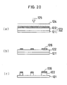
- a plate-making process relying upon another electrophotographic technique, wherein a photosensitive material 123 comprising a photoconductive material layer 122 and a grained aluminium plate 121 is first electrostatically charged by corona discharge in a uniform fashion, then pattern exposed to light 125 having a given wavelength through a film 124 (Fig. 20a) and finally coated with a toner 126, whereby the toner 126 is deposited onto a portion of the material 123 that has not been exposed to the light 125. After that, the toner 126 is fixed in place (Fig.
- the plate-making process shown in Fig. 17 should use a highly sensitive type of resin, because it resorts to exposure to ultraviolet rays.
- a class of material highly sensitive to ultraviolet rays are so poor in thermal stability that it is likely to suffer the so-called "thermal fogging”.
- the highly sensitive type of resin on the other hand, has a molecular weight so low that it offers a problem in connection with the resistance to printing required, i.e., the mechanical strength that printing plates are required to have.
- considerable difficulty will be encountered in finding a type of material that is satisfactory in terms of both sensitivity and resistance to printing.
- the printing substrate shown in Fig. 18 can be made more sensitive by the use of silver emulsions and can use conventional types of resin for the resin layer 106.
- this has a serious defect of being costly.
- photoconductive material layers are obtained by dispersing such photoconductive pigments as zinc oxide in polymeric materials.
- photoconductive pigments as zinc oxide
- they should contain zinc oxide in so large an amount, say 80 % in weight ratio, that they become fragile and lack in resistance to printing.
- a major problem with the latter "duplication assembly” is that it takes much time and expense to make duplicates, although the presetting of color scanner's separation conditions is achievable in a single operation.
- the present invention seeks to provide a printing plate that is well resistant to printing but dispenses with any transfer process by forming a toner image directly on a charge carrier medium and a method for making it.
- Another object of this invention is to provide a page make-up system using a charge carrier medium, wherein page-making-up is performed directly on a charge carrier medium by exposure with the application of voltage, thereby boosting the efficiency of page make-up operation.
- the above-described first object is attained by the provision of a printing plate using a charge carrier medium, characterized by including a printing area on an electrically conductive substrate, said printing area being constructed from a charge carrier layer and a toner layer.
- the printing plate using a charge carrier medium according to this invention which includes on an electrically conductive substrate a printing area defined by a charge carrier layer and a toner layer, has the following effects.
- the charge carrier medium which is not required to have photosensitivity or photoconductivity in itself and serves its own purpose if only it retains charges within a short time to development, may be formed of any one excelling in resistance to printing and resolution, chosen among a wide class of materials. In general, photosensitive- or photoconductivity-free materials may be given excellent resistance to printing, since their mechanical strength may be increased.
- non-image area may be made of a highly hydrophilic base metal material used with generally available planographic printing plates. This contributes to improvements in workability, since sufficient water retention is achieved with easy control of dampening water during printing, etc.
- the printing area is so covered with a toner layer that its lipophilic nature is on a sufficient level, its ink receptivity at the initiation time of printing is satisfactory, thus enabling high-quality prints to be obtained from just after the beginning of printing.
- high printability will still be obtained without weakening because of the charge carrier layer underlies the toner layer.
- the method for making printing plates using charge carrier media is characterized by including: a first step of applying voltage between a charge carrier medium comprising an electrically conductive substrate and a charge carrier layer and a photosensitive material to exposing said photosensitive material to a given pattern, thereby forming an electrostatic latent image having a given pattern on said charge carrier layer; a second step of toner-developing and fixing said electrostatic latent image on said charge carrier layer, obtained at said first step, and a third step of removing all portions of said charge carrier layer but the toner image obtained at said second step.
- photosensitivity is born by the photosensitive material while resistance to printing is done by the charge carrier medium.
- the functions of photosensitivity and resistance to printing can be separated from each other, enabling the material used to be selected from a wide range of materials.
- the exposure system with the application of voltage is so highly sensitive that it can be spectrally sensitive to the wavelength of laser light by selecting the type of photosensitive material.
- this system has an additional advantage of being able to use inexpensive light sources such as tungsten lamps.
- a projection type of exposure can be carried out with this system, making it possible to project an original plate of small size on an enlarged scale and reduce storage space.
- the page make-up system using a charge carrier medium is characterized in that: a photosensitive material is located in opposition to a charge carrier medium; an original image is exposed to light and projected through said photosensitive material on a given position at a given magnification and in a given direction, while a given voltage is applied between said photosensitive material and said charge carrier medium, whereby said image of the original is formed on said charge carrier medium in the form of an electrostatic latent image; and charges of said electrostatic latent image are read by a read sensor.
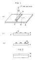
- reference numeral 1 stands for a photosensitive material, 2 a charge carrier medium, 3 a member for supporting the photosensitive material, 4 an electrode incorporated in the photosensitive material, 5 a photoconductive layer, 6 a charge carrier layer, 7 an electrically conductive substrate, and 8 a power source.
- an electrostatic latent image is first formed on the charge carrier layer 6 by exposure with the application of voltage.
- the photosensitive material 1 is first prepared by forming the electrode 4 and the layer 5, both in film forms, on the support 3 in that order.
- the photoconductive layer 5 of the material 1 is located in opposition to the charge carrier layer 6 of the charge carrier medium 2 with a given distance of d between them, said medium 2 being prepared by providing on the conductive substrate 7 said layer 6 in a film form.
- exposure may be carried out in a pattern exposure fashion wherein, as illustrated in Fig. 1(c), given light 11 is allowed to be incident all over the surface of a film 10 having a predetermined pattern, which is spaced away from the support 3 at a suitable interval or brought in close contact with it.
- exposure may be performed by scanning the film 10 with laser light 12 in a direction shown by an arrow 13, as shown in Fig. 1(d).
- the second type of exposure may also be implemented without recourse to such a film original 10 as shown in Fig. 1(d), i.e., by using the laser light 12 which has been modulated by image data made up by means of a color scanner.
- the material 1 may be scanned with light from a laser light source 17 along a line, shown at 14, and only over an angular range defined by ⁇ - main scanning, while it is moved and sub-scanned in a direction shown by an arrow 15 or in the opposite direction with keeping a distance d between it and the charge carrier medium 2 as predetermined.
- the charge carrier medium 2 is disconnected from the power source 8. Then, toner is coated on the charge carrier layer 6 for development, followed by toner fixation by heating.
- the electrostatic latent image formed on the charge carrier layer 6 takes shape as a toner image 16, as depicted in Fig. 1(f).
- a toner-free region is etched out of the charge carrier layer 6 by suitable means, using the toner image 16 as a mask, whereby a printing area-bearing, printing plate constituted by the toner 16 and the charge carrier layer 6 can be obtained on the electrically conductive substrate 7.
- the photosensitive material-supporting member 3 may be made of transparent materials through which active light for the photoconductive layer 5 is transmissible, such as various kinds of transparent glass, e.g. usual glass, quartz glass, non-alkali glass and Pyrex®; transparent thermoplastic resins, e.g. acrylic resin, polycarbonate, polyester, polystyrene, polyethylene and polypropylene; and transparent heat-curable resins, e.g. epoxy resin and polyimide resin.
- the support 3 may be 10 ⁇ m to 10 mm in thickness, and may have a thickness of 0.3 mm to 10 mm, especially when it is formed of a glass, acrylic or polycarbonate sheet. Also, when the support is formed of such a film as a polyester or polyimide film, it may have a thickness lying in the range of 10 to 500 ⁇ m.
- the support 3 used may be in flat or other forms. As shown in Fig. 1(e), it may be formed into a virtually semi-cylindrical shape. In this case, the semicircle may have a radius lying in the range of 1 to 50 mm.
- sheets of a material of 1 mm in thickness and having relatively high rigidity such as glass or resin, e.g., acrylic or polycarbonate resin, should have preferably been pre-processed into a desired semi-cylindrical shape, although varying with the rigidity of the support and photoconductive materials or the semicircle's radius.
- Such films as polyester films may be transformed into a cylindrical shape to form an electrode and a photoconductive layer. Alternatively, they may be cut out or otherwise shaped in a semi-cylindrical form of suitable size, after the formation of a flat or coiled type of electrode and photoconductive layer.
- those composed mainly of organic materials in particular are generally of flexibility, so that when used in combination with flexible supports formed of, e.g. polyester, they can be easily formed into a semi-cylindrical shape after having been provided with a flat- or coiled-form of electrode and photo-conductive layer.
- inorganic photosensitive materials such materials as typified by amorphous silicon and selenium are usually formed into films by CVD, vacuum deposition or other techniques in the absence of any binder. Because photoconductive layers are less flexible, however, their film thickness should preferably be reduced to 3 ⁇ m or below, when they are transformed into a semi-cylindrical shape after the formation of a flat or coiled type of electrode and photoconductive layer on flexible supports such as polyimide or polyester film supports.
- Some inorganic photosensitive materials including cadmium sulfide or zinc oxide powders have been mixed with organic binders, coated and formed into photosensitive layers. Their flexibility lies halfway between those of the above-mentioned organic photosensitive materials and amorphous silicon or selenium photosensitive materials. Thus, they can be processed into a semi-cylindrical shape, if it is 2 mm or more in radius, with no practical difficulty. It is then unnecessary to make photosensitive layers thin.
- the electrode 4 may be a an electrically conductive film made of such materials as tetracyanoquinodimethane and polyacetylene, a transparent electrode formed of such metal oxides as ITO, ZnO and SnO2, or a transparent electrode formed of thin films of such metals as Au, Pt and Pd, all being about 100 to 1,000 angstroms in thickness and 10 to 1,000 ⁇ / ⁇ in plane resistance value.
- the electrode 4 may be prepared in conventional manners, e.g., by plating, sputtering, vacuum deposition, CVD and coating followed by heat treatments, and may be transparent to active light for the photoconductive layer 5.
- the photoconductive layer 5 Upon irradiated with light, the photoconductive layer 5 generates photocarriers (electrons, positive holes) from the irradiated site, which can migrate widthwise there-through.
- the layer 5 is more effective esp. in the presence of an electric field.
- the layer 5 may be formed of an inorganic photoconductive material, an organic photo-conductive material, a composite inorganic/organic type of material, and so on.
- the inorganic photosensitive materials used may include amorphous silicon, amorphous selenium, cadmium sulfide, zinc oxide and the like.
- the amorphous silicon type of photosensitive material may include:
- These materials may have not been doped with impurities; have been converted into P types (hole transfer types) by doping with such elements as B, Al, Ga, In and Ti; and have been converted into N types (electron transfer types) by doping with such elements as P, Ag, Sb and Bi.
- silane and impurity gases may be introduced with hydrogen gas, etc. into a low-vacuum atmosphere (10 ⁇ 2 to 1 Torr) to deposit them on electrode substrates heated or not heated by glow discharge into films, or may be formed on simply heated electrode substrates through thermochemical reactions.
- the starting solid feed may be formed into films by vapor deposition or sputtering.
- the obtained films may be used in the form of a single or laminated films.
- the films may have a thickness of 1 to 50 ⁇ m.
- the electrode 4 may additionally be provided on its surface with a charge blocking layer which, when not exposed to light, serves to prevent charges from being injected , as the photoconductive layer were exposed to light from the elecgtrode 4.
- a charge blocking layer which, when not exposed to light, serves to prevent charges from being injected , as the photoconductive layer were exposed to light from the elecgtrode 4.
- an insulating layer or layer such as s-SiN, a-SiC, SiO2 and Al2O3 layers may be formed on one or both of the electrode substrate and the uppermost (surface) layer of the photosensitive material by glow discharge, vapor deposition, sputtering or other suitable means.
- the insulating layer is required to have a thickness of at most 1,000 angstroms, since too increased a thickness prevents an electric current from passing through it, when exposed to light. In view of the ease with which the insulating layer is prepared, etc. it may preferably lie in the thickness range of about 400 to 500 angstroms.
- the electrode substrate is preferably provided a charge transport layer capable of transporting charges of polarity opposite to that of the electrode substrate, making use of rectifying effects. If the electrode is negative, then a hole transport layer may be provided, and if the electrode is positive, then an electron transport layer may be provided.
- a-Si:H(n+) wherein Si is doped with boron has hole transport properties so increased that it produces rectifying effects, and so functions as a negative charge blocking layer.
- the amorphous selenium type of photosensitive material includes (i) amorphous selenium (a-Se), (ii) amorphous selenium tellurium (a-Se-Te), (iii) amorphous arsenic selenium (a-As2Se3), (iv) amorphous arsenic selenium + Te (a-As-Se-Te) or the like.
- This type of photosensitive material may be prepared by vapor deposition or sputtering, and an SiO2, Al2O3, SiC or SiN layer may be formed on an electrode substrate as the charge blocking layer by vapor deposition, sputtering, glow discharge or other suitable means.
- the above-described substances (i) to (iv) may be used in combination and formed into a laminated type of photosensitive material.
- This type of photosensitive layer may be similar in thickness to the amorphous silicon type of photosensitive material.
- This type of photosensitive material may be prepared by coating, vapor deposition or sputtering.
- solid particles of CdS may be placed on a tungsten board and vapor-deposited thereon by resistance heating or EB (electron beams).
- CdS targets may be used for deposition on substrates in argon plasma. In this case, CdS is usually deposited in an amorphous state, but it may be possible to obtain crystalline, oriented films (oriented in the thickness direction) by selecting the sputtering conditions.
- CdS particles having a particle size of 0.1 to 1 ⁇ m
- dispersed in binders with the addition of solvents may be coated on substrates.
- binders use may then be made of various types of resin, e.g. silicone resin, styrene-butadiene copolymer resin, epoxy resin, acrylic resin, saturated or unsaturated polyester resin, polycarbonate resin, polyvinyl acetal resin, phenolic resin, polymethyl methacrylate (PMMA) resin, melamine resin and polyimide resin.
- resin e.g. silicone resin, styrene-butadiene copolymer resin, epoxy resin, acrylic resin, saturated or unsaturated polyester resin, polycarbonate resin, polyvinyl acetal resin, phenolic resin, polymethyl methacrylate (PMMA) resin, melamine resin and polyimide resin.
- silicone resin e.g. silicone resin, styrene-butadiene copolymer resin, epoxy resin, acrylic resin, saturated or unsaturated polyester resin, polycarbonate resin, polyvinyl acetal resin, phenolic resin, polymethyl methacrylate (PMMA) resin, melamine
- the amount of CdS to be added may lie in the binder to CdS range of 1:3 to 1:1 in weight ratio.
- This CdS type of photosensitive material may be coated on semi-cylindrical substrates by not only dip or cast coating but also blade coating making use of a blade located with a suitable gap between it and the substrates.
- the resulting films may have a thickness lying in the range of 3 to 100 ⁇ m.
- This type of photosensitive material may be prepared by coating or CVD.
- ZnO particles having a particle size of 0.1 to 1 ⁇ m
- binders with the addition of solvents
- binders use may then be made of various types of resin, e.g. silicone resin, styrene-butadiene copolymer resin, epoxy resin, acrylic resin, saturated or unsaturated polyester resin, polycarbonate resin, polyvinyl acetal resin, phenolic resin, polymethyl methacrylate (PMMA) resin, melamine resin and polyimide resin.
- resin e.g. silicone resin, styrene-butadiene copolymer resin, epoxy resin, acrylic resin, saturated or unsaturated polyester resin, polycarbonate resin, polyvinyl acetal resin, phenolic resin, polymethyl methacrylate (PMMA) resin, melamine resin and polyimide resin.
- silicone resin e.g. silicone resin, styrene-butadiene copolymer resin, epoxy resin, acrylic resin, saturated or unsaturated polyester resin, polycarbonate resin, polyvinyl acetal resin, phenolic resin, polymethyl methacrylate (PMMA) resin, melamine
- the amount of ZnO to be added may lie in the binder to ZnO range of 1:3 to 1:10 in weight ratio.
- the resulting films may have a thickness lying in the range of 3 to 100 ⁇ m.
- This type of photosensitive material may be coated on semi-cylindrical substrates in similar manners as used with the cadmium sulfide type of photosensitive material.
- CVD such organic metals as diethyl zinc and dimethyl zinc are mixed with oxygen gas in a low-vacuum atmosphere (10 ⁇ 2 to 1 Torr), and the resulting mixture is then subjected to chemical reactions on electrode substrates heated (to 150 to 400°C), whereby it is deposited thereon in the form of a zinc oxide film, which is again oriented in the thickness direction.
- the organic photosensitive material is broken down into single-layer and function-separated types.
- the single layer type of photosensitive material comprises a mixture of a charge generating substance with a charge transporting substance.
- Belonging to this system are a class of substances likely to absorb light to generate charges.
- Usable to this end are azo pigments, bisazo pigments, trisazo pigments, phthalocyanine pigments, perylene pigments, pyrylium dyes, cyanine dyes and methine dyes.
- Belonging to this system are a class of substances capable of well transporting ionized charges.
- Usable to this end for instance, are hydrazones, pyrazolines, polyvinyl carbazoles, carbazoles, stilbenes, anthracenes, naphthalenes, tridiphenylmethanes, azines, amines and aromatic amines.
- Charge-transfer complexes may also be formed from the charge-generating and -transporting substances.
- PVK polyvinyl carbazole
- TNF trinitrofluorenone
- Such a single layer type of photosensitive films may preferably have a thickness of 10 to 50 ⁇ m.
- charge-generating substances are likely to absorb light but have the property of trapping charges, whereas the charge-transporting substances have superior charge-transporting characteristics but are inferior in terms of light absorption. For that reason, both the substances are separated from each other to make much use of their respective properties. Thus, charge-generating and -transporting layers are laminated together.
- the substances forming the charge generating layers may include compounds based on azo, bisazo, trisazo, phthalocyanine, acid xanthene dye, cyanine, styryl pigment, pyrylium, perylene, methine, a-Se, a-Si, azulenium salt and squalenium systems.
- the substances forming the charge transporting layers include compounds based on hydrazone, pyrazoline, PVK, carbazole, oxazole, triazole, aromatic amine, amine, triphenylmethane and polycyclic aromatic systems.
- the charge generating substance is first dissolved or dispersed with solvents in binders, and the resulting coating solution is then coated on electrodes by means of rotary coating, roll coating, wire bar coating, blade coating, spray coating, dip coating or other suitable technique. After that, the charge transporting substance is dissolved with solvents in binders, and the resulting coating solution is then likewise coated on the charge generating layer.
- the resulting charge generating layer may have a thickness of 0.1 to 5 ⁇ m, while the charge transporting layer may be 2 to 50 ⁇ m in thickness.
- Binders used for both the single-layer and function-separated types of photosensitive materials include various forms of resin, e.g. silicone resin, styrene-butadiene copolymer resin, epoxy resin, acrylic resin, saturated or unsaturated polyester resin, polycarbonate resin, polyvinyl acetal resin, phenolic resin, polymethyl methacrylate (PMMA) resin, melamine resin and polyimide resin.
- resin e.g. silicone resin, styrene-butadiene copolymer resin, epoxy resin, acrylic resin, saturated or unsaturated polyester resin, polycarbonate resin, polyvinyl acetal resin, phenolic resin, polymethyl methacrylate (PMMA) resin, melamine resin and polyimide resin.
- the binder should be used in an amount of 0.1 to 10 parts per part of each of the charge-generating and -transporting layers. Coating may be achieved by not only the above-mentioned wet coating processes but dry coating processes as well, e.g
- the function-separated type of photosensitive material is not critical as to which of the charge-generating or -transporting layer is to be first laminated on a transparent electrode. Because exposure occurs from the side of the electrode, it is preferable that when use is made of a charge transporting layer less transparent to active light used for exposure, the charge generating layer be first formed on the electrode.
- the charge blocking layer may be provided on at last one or both sides of the photoconductive layer 5 so as to prevent a dark current (the injection of charges from the electrode) from passing through it, i.e., a phenomenon that even when not actually exposed to light, charges migrate through the photoconductive layer, as if it were exposed to light.
- the charge blocking layer is of two types, one making use of an insulting thin film and the other relying upon rectifying effects.
- first type of layer making use of an insulating thin film mere application of voltage does not allow currents to pass through the photoconductive layer or reach the surface of the resin layer due to its presence.
- a high electric field is applied to its site exposed to light due to the presence of one (electron or hole) of the charge generated in the photoconductive layer, so that currents can pass through the photoconductive layer by way of the charge blocking layer.
- Such a charge blocking layer may be formed of an inorganic insulating film, an insulating, organic polymeric film or an insulating monomolecular film, which may be used alone or laminated together for use.
- the inorganic insulating film may be obtained by As2O3, B2O3, Bi2O3, CdS, CaO, CeO2, Cr2O3, CoO, GeO2, HfO2, Fe2O3, La2O3, MgO, MnO2, Nd2O3, Nb2O5, PbO, Sb2O3, SiO2, SeO2, Ta2O5, TiO2, WO3, V2O5, Y2O5, Y2O3, ZrO2, BaTiO3, Al2O3, Bi2TiO5, CaO-SrO, CaO-Y2O3, Cr-SiO, LiTaO3, PbTiO3, PbZrO3, ZrO2-Co, ZrO2-SiO2, AlN, BN, NbN, Si3N4, TaN,
- this layer may be determined for each material, while taking into consideration the insulating properties for preventing the injection of charges. Usually, however, it may be selected from the range of 0.01 to 10 ⁇ m, preferably 0.05 to 1 ⁇ m.
- a charge transporting layer capable of transporting charges through such effects and having polarity opposite to that of an associated electrode.
- a charge blocking layer is may be formed of an inorganic photoconductive layer, an organic photoconductive layer or a composite inorganic/organic type of photoconductive layer, and may have a film thickness of about 0.1 to 10 ⁇ m.
- an amorphous silicon photoconductive layer doped with B, Al, Ga, In, etc. or an organic photoconductive layer formed by dispersing in resin amorphous selenium or such a compound as oxadiazole, pyrazoline, polyvinyl carbazole, stilbene, anthracene, naphthalene, tridiphenylmethane, triphenylethane, azine, amine or aromatic amine.
- the distance d may be about 10 ⁇ m.
- d may be zero; the photoconductive layer 5 may be in close contact with the charge carrier layer 6.
- the electrically conductive substrate 7 must function as an electrode during voltage application and exposure, and should be made hydrophilic at least on its surface for use as a planographic printing plate. Usable to this end is an about 0.3-mm thick, grained aluminium plate. Thus, to use a grained aluminium plate as the electrically conductive substrate 7 is found to be particularly advantageous for large-area printing. As shown in Fig. 2, however, a 1000-angstrom to 1- ⁇ m thick, aluminium film layer 19 formed on an insulating substrate 18 formed of glass, etc. as by vapor deposition may be used for obtaining small-area prints, nearly the size of postcards. Zinc may be used in place of aluminium.
- the charge carrier layer 6 Essentially required for the charge carrier layer 6 are that not only is it capable of retaining charges, but it is removable by suitable etching and needs to be enough hydrophilic to form a printing area and to have resistance to printing or, in a better word, mechanical strength. For instance, such materials as will be described later may be used. It is understood that the charge carrier layer 6 may have a thickness of about 2 to 10 ⁇ m.
- the charge carrier layer 6 needs to have enough insulating properties to limit migration of charges, say, a specific resistance that is at least as high as 1014 ⁇ /cm.
- a charge carrier layer 6 may be prepared by dissolving various types of rubber or resin in solvents, followed by coating, dipping, vapor deposition or sputtering.
- the types of resin and rubber used in this invention may include polyethylene, polypropylene, vinylic resin, styrol resin, acrylic resin, nylon 66, nylon 6, polycarbonate, acetal homopolymer, fluoroplastic, cellulose resin, phenolic resin, urea resin, polyester resin, epoxy resin, flexible epoxy resin, melamine resin, silicon resin, phenoxy resin, aromatic polyimide, PPO and poly-sulfone; and polyisoprene, polybutadiene, polychloroprene, polar nitrile, polyacrylic rubber, chlorosulfonated poly-ethylene, ethylene/propylene rubber, fluororubber, silicone rubber, polysulfide-based synthetic rubber and urethane rubber, all being used alone or in admixture.
- cellulose acetate succinate half-ester and polyvinyl pyridine (as an elutant for them an aqueous solution of dilute alkali may be usable; the bracketed compounds shall hereinafter refer to elutants); partially saponified polyvinyl acetate (water); partially saponified polyvinyl acetate/ethylene oxide adduct and polyvinyl pyrrolidone (water); polyurethane polyene (a dilute aqueous alkaline solution); an unsaturated type of polyester using a polyethylene glycol wherein n is at least 6, such as a polyethylene glycol/adipic acid/fumaric acid polycondensate or an unsaturated type of polyester modified by such diisocyanatos as toluene diisocynato and phenylene diisocyanato (an aqueous solution of dilute alkali); an alcohol soluble type of polyvinyl pyridine (as an el
- the power source 8 may be operable at a d.c. voltage of 500 to 1,500 volts. For instance, if plus voltage is applied to the electrode 4, as shown in Fig. 1, then a positively charged pattern is formed on the charge carrier layer. This pattern may in turn be developed with negatively charged toner particles.
- the exposure light sources use may be made of laser light and ultraviolet rays. Use may also be made of visible light emanating from tungsten, halogen or other lamps. For instance, when an a-Se photosensitive material with a 30- ⁇ m thick a-Se laminated thereon is used on a 5,000-angstrom thick, a-SeTe charge generating layer, exposure may be carried out at about 50 luxes for 0.1 second, using tungsten lamp light having a color temperature of about 4,000°K.
- the wet and dry types of toners may both be used in this invention.
- the dry type of toner is so relatively large, say 10 to 30 ⁇ m, in particle size that it is inferior in terms of resolution, but the wet type of toner gives sufficient resolution because its particle size is small, say, about 0.1 to 3 ⁇ m.
- Toner fixation may be effected at such a temperature as set forth about a specific wet type of toner in Japanese Patent Kokai Publication No. Sho. 58-2851. Typically, it may occur at 100°C for about 2 to 5 minutes. It is understood that even with a general dry type of toner, toner fixation is achievable under the same conditions.
- all portions of the charge carrier layer but the toner image are removed by etching, using the fixed toner image as a resist.
- This etching may be achieved by removing all portions of the charge carrier layer except the toner image with solvents in which the charge carrier layer dissolves; or removing all portions of the charge carrier layer, which are not covered with the toner, by calcination with plasma calcination equipment, etc.
- a photo-decomposable type of resin for instance, a positive type of photoresist may be used as a charge carrier layer material.
- the charge carrier layer is irradiated with allover active light (e.g. ultraviolet rays), using the toner image as a light-shielding image, followed by development where all portions of the charge carrier layer, which are not covered with the toner, are removed.
- allover active light e.g. ultraviolet rays
- the electrode 7 is exposed to view. If required, such post-treatments as etching and rubberizing may be performed.
- a 0.3-mm thick aluminium sheet was grained on its surface by ball polishing, followed by washing of that surface with the following plane regulating liquid and water.
- the aluminium sheet was made hydrophilic with the following treating solution, washed with water and dried.
- this aluminium sheet was rotary coated thereon with a 5 % solution of an acrylonitrile/butadiene/acrylic acid polymer in toluene to a dry coverage of 3 ⁇ m. After that, the resulting film was dried in a 100°C oven for 30 minutes to obtain a plate.
- a 30- ⁇ m thick, a-Se layer was formed as a charge transporting layer by similar vacuum deposition to obtain a photosensitive material.
- this photosensitive plate was pressed onto the above-described plate with a local gap between them through a 9- ⁇ m thick polyester film. This gap was found to be 12 ⁇ m. Subsequently, a half tone or screen positive film of 150 lines per inch was brought into close contact with the photosensitive material. A voltage of + 800 v was applied to the electrode of the photosensitive plate, while the aluminium plate was earthed.
- the photosensitive plate was irradiated with substantially parallel light emanating from a tungsten lamp having a color temperature of 4,000°K at an illuminance of about 50 luxes, as measured thereon. After switched on for 0.1 second, the plate was removed.
- etching was carried out with a 5 % aqueous solution of sodium carbonate, followed by water washing and drying, thereby giving a planographic printing plate.
- a printing plate prepared by following the procedures of Ex. 1 was mounted on a web offset printing press to obtain 100,000 prints.
- the printing plate turned out to be not damaged.
- this is a view for illustrating how to record images with the charge carrier medium, wherein reference numeral stands for a charge carrier medium, 22 a photosensitive material and E a power source.
- the charge carrier medium 21, for instance, is constructed by forming a 1,000-angstrom thick Al film on an insulating layer support 21c comprising a 1-mm thick glass by vapor deposition to form an electrode 21b and providing a 10- ⁇ m thick insulating layer 21a on the electrode 21b.
- the photosensitive material 22 is constructed from a support 22a, an electrode 22b and a photoconductive layer 22c, as is the case with the photosensitive material 1 shown in Fig. 1.
- a support 22a comprising a 1-mm thick glass may be provided thereon with a 1,000-angstrom thick, transparent electrode of ITO, and an about 10- ⁇ m thick photoconductive layer 22c may then be formed on that electrode.
- FIG. 3 there is shown an embodiment wherein the charge carrier medium 21 is exposed to light through the photosensitive material 11.
- the charge carrier medium 21 is first spaced away from the photosensitive material 22 with a gap of about 10 ⁇ m between them.
- the power source E applies a given voltage between the the electrode 22b of the photosensitive material and the electrode 21b of the charge carrier medium, as shown in Fig. 3b. In the dark, there will be no change between both the electrode, due to the photoconductive layer 22c being a high resistance body.
- the power source E is disconnected off, as shown in Fig. 3c.
- the charge carrier medium 21 is removed, as shown in Fig. 3d, thereby completing the formation of an electrostatic latent image.
- the photosensitive material 22 and charge carrier medium 21 may be either located in a non-contact fashion, shown in Fig. 3, or arranged in a contact manner. When they are located in contact with each other, positive or negative charges are injected from the electrode 22b of the photosensitive material into the exposed region of the photoconductive layer 22c. These charges then pass through the photoconductive layer 22c under the attracting action of the electrode 21b and reaches the surface of the insulating layer 21 where charge transfer stops, thereby accumulating charges on that site. Subsequent separation of the charge carrier medium 21 from the photosensitive material 22 allows separation of the insulating layer 21a with charges remaining accumulated thereon.
- This type of recording when applied to planar analog recording, gives resolving power as high as does silver salt photographic techniques.
- the surface charges accumulated on the insulating layer 21a which are exposed to an air atmosphere, can be stored without discharge over extended periods of time regardless of whether that layer is placed in the dark or in the bright, since air can serve as a good insulator.
- the "charges" have been described as surface charges. However, it is noted that in some cases charges may build up only on the surface of an insulator; in some cases charges may penetrate through an insulator via its surface with the electrons or holes being trapped in the structure of that material. Thus, the charges can be stored over extended periods of time. In order to prevent discharge, etc. due to physical damage of the charge carrier medium or in high-humidity conditions, the insulating layer 21a may be covered on its surface with an insulating film, etc. for more stable storage.
- an original 25 is irradiated with light from a light source 23 or 24, and the resulting transmitting or reflected light strikes upon the surface of a photosensitive material 22 through a color filter 26 for recording on a charge carrier medium 21.
- the color filter 26 comprises three red (R), green (G) and blue (B) elements, and is designed to move horizontally for selection of R, G and B.
- a set of three charge carrier media are used to record one piece of color image information.
- Fig. 4b there is shown another embodiment of color image information recording, which is similar to that of Fig. 4a with the exception that a rotary type of color filter 27 is used for selection of R, G and B.
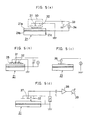
- FIG. 5a One example of how to read potential is illustrated in Fig. 5a wherein the same parts as in Fig. 3 are indicated by the same reference numerals.
- reference numeral 30 stands for a potential reader section, 31 a detection electrode, 32 a guard electrode, 33 a capacitor and 34 a voltmeter.
- the detection electrode 31 receives an electric field defined by the charges accumulated on the insulating layer 21a of the medium 21, generating on its surface induction charges in an amount equal to that of the charges on the medium 21. Since the capacitor 33 is charged with charges of polarity opposite to that of such induction charges in the same amount, there is a potential difference corresponding to the accumulated charges across the electrode of the capacitor 33, which is in turn read on the voltmeter 34, thereby determining the potential of the charge carrier medium 21. Then, an electrostatic latent image can be produced in the form of electrical signals by scanning the surface of the charge carrier medium 21 with the potential reader 31.
- Fig. 5b illustrates another system to read potential, which is similar to that illustrated in Fig. 5a, provided that potential is detected through an insulating protective film 35 on which detection and guard electrodes 31 and 32 are mounted.
- this system that is designed to come in contact with a charge carrier medium 21 for the detection of potential, it is possible to keep constant the space between the detection electrode 31 and the charge carrier medium 21.
- Fig. 5c is a view showing still other system of how to read potential, wherein a pin type of electrode 36 is brought in direction contact with a charge carrier medium 21 to detect the potential of the site of contact.
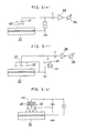
- Fig. 5b is an illustration of a vibration electrode type of potential reading system, wherein 37 is a detection electrode, 38 an amplifier and 39 a meter.
- the detection electrode 37 vibrates and is driven such that as time goes by, it displaces with respect to the charged surface of a charge carrier medium 21.
- potential across the detection electrode 37 varies with time at an amplitude corresponding to the electrostatic potential of the charged surface.
- This potential change with time is then obtained in the form of a voltage change appearing across an impedance Z, and the a.c. component is in turn amplified by the amplifier 39 through a capacitor C to measure the electrostatic potential of the charged surface in terms of readings on the meter 39.
- Figure 5e shows an example of a rotary detector, wherein a rotary blade is indicated at 40.
- a detection electrode 37 and the charged surface of a charge carrier medium 21 there is an electrically conductive rotary blade 40 driven for rotation by driving means, not illustrated.
- the detection electrode 37 is periodically and electrically shielded relative to the charge carrier medium 21.
- Potential signals varying periodically at an amplitude corresponding to the electrostatic potential of the charged surface is then detected by the detection electrode 37, and the A.C. component is in turn amplified by an amplifier 38 for reading.
- Fig. 5f is an illustration of a vibrating capacitance-reed detector, wherein reference numerals 41 and 42 stand for a driving circuit and a vibrating reed, respectively.
- the vibrating reed 42 of one electrode forming a capacitor is vibrated by the driving circuit 41 to change the capacitor's capacity.
- D.C. potential signals detected by a detector electrode 37 are modulated, and the A.C. component is then amplified and detected.
- this detector designed to convert direct currents to alternate currents. it is possible to measure potential with high sensitivity and good stability.
- Fig. 5g shows an example of a collector type of detector, in which reference numerals 43 indicates a grounded type of metallic cylinder, 44 an insulator and 45 a collector.
- the collector 45 contains a radioactive substance which emits ⁇ -rays. in the metallic cylinder, the air is thus ionized to form positive and negative ion pairs. Under natural conditions, these ions tend to disappear by recombination and diffusion until equilibrium is reached. In the presence of an electric field, however, they collide repeatedly with air molecules through thermal motion and migrate statistically toward the electrical field, thus playing a role of carrying charges. That is, for the reason that the air is made electrically conductive by ions, an equivalent electrical resistance path is taken as existing between the collector 45 and a surrounding object.
- V2 R2V1/(R1+R2) wherein: R1 is the resistance between the charged body and the collector 43, R2 is the resistance between the collector 45 and the grounded metallic cylinder 43, V1 is the potential of the charged body, and V2 is the potential of the collector 45.
- R1 is the resistance between the charged body and the collector 43
- R2 is the resistance between the collector 45 and the grounded metallic cylinder 43
- V1 is the potential of the charged body
- V2 is the potential of the collector 45.
- Fig. 5h is an illustration of an example of an electron beam type of potential reader system, in which reference numeral 46 denotes an electron gun, 47 electron beams, 48 a first diode and 49 a secondary electron amplifier section.
- Electrons leaving the electron gun 46 are deflected by an electrostatic or electromagnetic deflector, not shown, and scan the charged surface. Some of the scanning electron beams join to the charges of the charged surface into a charging current, and so the potential of the charged surface drops to equilibrium potential, correspondingly. Another portion of the beams is modulated and fed back toward the electron gun 46. In the meantime, they collide with the first diode 48. The resultant secondary electrons are amplified by the secondary electron amplifier 49 and obtained from the anode in the form of a signal output. As the return electron beams, reflected or secondary electrons may be used.
- Fig. 5i is an illustration of a further example of the potential reader system.
- a charge carrier medium 21, on which an electrostatic latent image has been formed, is toner-developed.
- the colored surface is then irradiated with light beams for scanning.
- the reflected light is converted to electrical signals by a photoelectric converter 50.
- Fig. 5j shows a still further example of the potential reader system.
- Color-separated images R, G and B formed by such a fine color filter as will be described later are toner-imaged.
- the colored surfaces are irradiated with light beams to convert the reflected light to signals Y, M and C.
- reference numeral 51 denotes a scanning signal generator, 52 a laser, 53 a reflector, 54 a half mirror, 58 a photoelectric converter and 55, 56 and 57 gate circuits.
- the colored surfaces are irradiated with laser beams from the laser 52 through the reflector 53 and half mirror 54 for scanning.
- the light reflected from the colored surfaces is then fed into the photoelectric converter 58 through the half mirror 54 to convert it to electrical signals.
- the gate circuits 55, 56 and 57 are controlled for opening or closing synchronously with the signals from the signal oscillator 51, then they are controlled for opening or closing synchronously with the pattern of the fine filter.
- Fig. 5k is an illustration of a still further example of potential reading, wherein an electrical line of force generated by electrostatic charges acts on an electro-optical material 130, and the resulting change is read by an optical sensor 131 through light 132.
- the electro-optical material 130 used may include LiNbO3 and liquid crystals.
- the light 132 may be deflected, if required, and the optical sensor 131 may contain a deflector, if desired.
- a charge carrier medium 21 is transparent.
- this system may be used with such an optical system as shown in Figs. 5i and 5k, thereby detecting reflected light.
- scanning may be effected with the charge carrier medium 21.
- scanning may be performed with the light 132 and optical sensor 131.
- an area sensor as CCD may be used as the optical sensor 131, thereby focusing an image on the area sensor through a lens.
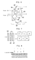
- FIG. 6 there is shown a prismatically color-separating, optical system 68 in which reference numerals 60, 61 and 62 stand for prism blocks, 63, 64 and 65 filters and 66 and 67 reflectors.
- the color-separating, optical system 68 is constructed from three prism blocks 60, 61 and 62. Optical information incident on a plane a of the prism block 60 is partly separated and reflected from a plane b , giving an optical component of color B through the filter 63. The rest of the optical information is incident on the prism block 61 and reaches a plane c from which it is partly separated and reflected. Another portion reaches directly the filter 65 from which optical components of colors G and R are obtained. The optical components of colors G and B may then be reflected from the reflectors 66 and 67, giving the R, B and B light components in the form of parallel light beams.
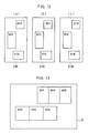
- one frame may be formed either by three sets of charge carrier media separated into R, G and B colors, as shown in Fig. 7b, or by a set of R, G and M images arranged on one plate, as illustrated in Fig. 7b.
- Fig. 8 is an illustration of one fine color filter.
- this may be formed by exposing a resist-coated film to light through a mask pattern to form R, G and B striped patterns, which are then dyed in R, G and B; passing light components separated with the system of Fig. 6 through fine slits to obtain R, G and B interference fringes, which are then recorded in a hologram recording medium; or forming R, G and B striped patterns with electrostatic latent images, which are then toner-developed and transferred three times for color synthesis, thereby forming toner stripes.
- a set of R, G and B forms one picture element as fine as about 10 ⁇ m. If this filter is used as the color-separating, optical system 68 of Fig. 7, it is then possible to form a color, electrostatic latent image. In this case, the filter may be spaced away from or made integrate with the photosensitive material.
- Figure 9 is a view showing one example of the fine color filter combined with a Fresnel lens, in which R, G and B patterns may be reduced in size by the Fresnel lens for recording and lens designs may be made more compact and thinner than conventional lens ones.
- Fig. 10 is a view showing one example of three-plane splitting in which half mirrors are used in combination with R, G and B filters. Incident light is split into three portions through half mirrors 71 and 72 and a reflector 73, which are then allowed to pass through R, G and B filters 74, 75 and 76, respectively, giving R, G and B components of light in the form of parallel light beams.
- the electrostatic latent images formed on the charge carrier medium may be erased by:
- a charge carrier medium 21 and a photosensitive material 22 are provided prior to page make-up work.
- the photosensitive material 22 is exposed to light through an original image 80 and a suitable lens system 81 at such a magnification as prescribed by an associated layout sheet, say, on a full-size scale in the instant example, whereby an electrostatic latent image corresponding to the original image 80 is formed on a given position of the charge carrier medium 21. If this cycle is repeated for all originals assigned to said layout sheet, it is then possible to effect page make-up for the originals used on said layout sheet.
- the sizes of the charge carrier medium 21 and photosensitive material 22 may be such that the original images can be exposed to light according to the prescribed size, say, the full size in this example.
- the full-size image data are processed in an image processor for density regulation, tone adjustment, trimming and other purposes. Finally, that data can be output through a color scanner on a film.
- the charge carrier medium 21 and photosensitive material 22 that are of the same size as that of the layout sheet, because all the original images used on the associated page can be laid out by projection on the position prescribed on the associated layout sheet. It is understood that the projection of the original images may preferably be carried out in a range larger than the trimming range prescribed on the layout sheet.
- the projection of the original images on the position prescribed on the layout sheet at the prescribed magnification and in the prescribed direction may be achieved by using conventional equipment, e.g. an image projector.
- the original images on the layout sheet on a full-size scale, i.e., the size prescribed on the layout sheet.
- the original images projected is a matter of choice. For instance, they may be projected on a scale reduced to a half the prescribed size; however, this offers various problems.
- the prescribed magnification may immediately be used if the original images are projected a full-size scale. Whenever they are projected on a reduced scale, however, it is required to fix the magnification at 1/2, and this is likely to give rise to an error in magnification setting. This is even so especially when exposure is again carried out after the once obtained electrostatic latent image has been erased.
- the image data may immediately be used not only for the image processing to be described later but also for exposure of an output film through a color scanner.
- the image data In the case of exposure on a reduced scale, however, the image data must be enlarged for output to the film, and this does not only incur an extra time for image processing but also cause cost rises due to the need of using hardware for enlargement processing. Although such timeconsuming work and cost rises may be negligible, it would be clear that the image exposed on a full-size scale outclasses the image exposed on an enlarged scale.
- Full-size exposure is also more advantageous in reading the potential of the charge carrier medium. This is because, for the reason that exposure on a reduced scale must eventually be followed by enlargement processing, the density of the picture elements read must be made higher than that in the case of full-scale exposure, with attendant increases in the cost of the reading head.
- the red, green and blue, electrostatic latent images may be formed on three charge carrier media 21 R , 21 G and 21 B , respectively, with the procedure shown in Fig. 6 or 10.
- the striped color-filter may be used to form such electrostatic latent images with the procedure shown in Fig. 8.
- the quantity of misalignment among the color-separated images matches the quantity of relative color mismatching with respect to the colors of the striped filter, thus depending upon the positional accuracy of the striped filter. This implies that if the striped filter is located in place, there will be no color mismatching in principle.
- mechanical registration must be effected with high accuracy.
- the pitch of three-colored or R, G and B stripes may be made fine to the required resolution.
- one side of one picture defined by three colors R, G and B may be up to 50 ⁇ m in length, because the resolution capable of outputting a dot image of 175 lines per inch is said to be more than 500 lines per inch.
- Color character reading should be much higher in resolution than color image reading, and so should have a resolution of 1,200 to 2,400 lines per inch.
- the striped color-filter pitch may be determined such that picture elements of about 20 to 10 ⁇ m in size are obtainable.
- electrostatic latent images of the original images can be formed on the prescribed position on a layout sheet according to the prescribed size. It is understood, however, that if the objective is only to form a full-scale electrostatic latent image irrespective of position, an array of, G and B electrostatic latent images of one original image may be formed on one charge carrier medium 21 in side-by-side relation.
- reference numerals 85, 86, 87, 88 and 89 stands for the originals, respectively
- 85 R , 85 G and 85 B represent red, green and blue images of the original 85, respectively.
- a given position on the charge carrier medium may be exposed to light through the individual originals.
- other regions should be protected against fog, etc.
- exposure may be effected, while said other regions are masked.
- a given voltage may be applied to only the region to be exposed of an arrangement wherein an electrode 22b of the photosensitive material and an electrode 22b of the charge carrier medium, both in striped forms, are designed to intersect each other at nearly right angles.
- the potentials of said electrostatic latent images are read with any one of the potential reading systems shown in Fig. 5, and are then fed to a suitable image processor in the form of electrical signals, where such image processings as trimming, density regulation or tone adjustment are done, if required. Finally, the output is fed to a color scanner for output to a film.
- Fig. 14 shows one system designed to this end.
- a reader 90 the electrostatic latent images recorded on a charge carrier medium 21 are read. More specifically, the electrostatic latent images recorded on the charge carrier medium 21 are read by a reading head 92, with any one of the above-described systems for reading electrostatic latent images.
- the analog data readings are fed through an amplifier 93 wherein they are amplified into an image processor 91. In this image processor 91.
- the R, G and B analog data fed out of the reader 90 are converted through a digital convertor 94 into digital data of given bits, followed by such processings as trimming and color conversion. In Fig. 14, trimming, color conversion and muddiness correction occur in that order.
- a trimmer 95 is used to extract only the range prescribed by the layout sheet from the images data of the respective originals.
- a color convertor 96 is provided to convert the R, G and B data into C, M, Y and K data.
- the C, M, Y and K data obtained through the color convertor 96 are then corrected for muddiness by a muddiness corrector 97, wherein they are converted into C', M', Y' and K' in consideration of ink's muddiness, thereby avoiding printed images' muddiness due to ink's muddiness.
- the data corrected for muddiness are then subjected to dot processing in a dot processor 98.
- Dot processing may be achieved by varying the size of dots depending upon the density of images, as shown in Fig. 15.
- Fig. 15a shows a highlight or white tone array of dots;
- Fig. 15b a gray or 50 % tone array of dots;
- Fig. 15c a black or shadow tone array of dots.
- dot processing is achieved by varying the size of dots depending upon the density of images but without varying the pitch of dots.
- Dot formation may be done by a procedure resorting to a dot generator, as shown in Fig. 16. This procedure will now be explained schematically.
- a dot generator as shown in Fig. 16.
- This procedure will now be explained schematically.
- the density level of an image corresponding to one dot is found at 8, as shown in Fig. 16b.
- the weight value is compared with the image level of 8 to make black zones whose density level exceeds the weight value, as shown by hatched zones in Fig. 16c. It is thus possible to form dots of size corresponding to the density level.
- the image data subjected to dot processing is exposed to light by an exposure unit 99 based on the results of dot processing, and then fed to a color scanner (not shown) wherein a film wound around an input drum is exposed to light.
- Fig. 14 shows only the flow of signal processing.
- the system may include a memory for storing digitally converted image data, image data obtained as a result of dot processing or the like, display means such as color CRTs, input units such as keyboards or mouses, and so on.
- the present printing plates using charge carrier media, method for making them and page make-up systems using charge carrier media have wide applications in the field of making printing plates and page make-up systems.
Landscapes
- Physics & Mathematics (AREA)
- General Physics & Mathematics (AREA)
- Photoreceptors In Electrophotography (AREA)
Applications Claiming Priority (4)
| Application Number | Priority Date | Filing Date | Title |
|---|---|---|---|
| JP245430/89 | 1989-09-21 | ||
| JP24543089 | 1989-09-21 | ||
| JP299168/89 | 1989-11-17 | ||
| JP29916889A JPH03158867A (ja) | 1989-11-17 | 1989-11-17 | 電荷保持媒体を用いた集版システム |
Publications (2)
| Publication Number | Publication Date |
|---|---|
| EP0444211A1 true EP0444211A1 (de) | 1991-09-04 |
| EP0444211A4 EP0444211A4 (en) | 1993-03-17 |
Family
ID=26537225
Family Applications (1)
| Application Number | Title | Priority Date | Filing Date |
|---|---|---|---|
| EP19900913869 Withdrawn EP0444211A4 (en) | 1989-09-21 | 1990-09-19 | Printing press using charge retaining medium, its manufacturing method and stripping system using charge retaining medium |
Country Status (2)
| Country | Link |
|---|---|
| EP (1) | EP0444211A4 (de) |
| WO (1) | WO1991004518A1 (de) |
Family Cites Families (8)
| Publication number | Priority date | Publication date | Assignee | Title |
|---|---|---|---|---|
| BE598591A (de) * | 1959-12-28 | |||
| JPS597387B2 (ja) * | 1978-03-22 | 1984-02-17 | 大日本印刷株式会社 | 平版印刷用刷板の製造方法 |
| US4628017A (en) * | 1984-11-02 | 1986-12-09 | Ricoh Company, Limited | Electrostatic image forming method |
| JPS6149895A (ja) * | 1985-06-24 | 1986-03-11 | Konishiroku Photo Ind Co Ltd | 印刷板の形成方法 |
| JPS62109062A (ja) * | 1985-11-07 | 1987-05-20 | Ricoh Co Ltd | 電子写真製版用印刷原版 |
| EP0281727B1 (de) * | 1987-03-09 | 1993-09-08 | Mitsubishi Paper Mills, Ltd. | Herstellungsverfahren von lithographischen Druckplatten, Verwendung einer derartigen Druckplatte zum Drucken und Druckverfahren mit einer derartigen Druckplatte |
| CA1339152C (en) * | 1988-05-17 | 1997-07-29 | Dai Nippon Printing Co., Ltd. | Electrostatic information recording medium and electrostatic informationrecording and reproducing method |
| DE69023042T2 (de) * | 1989-03-24 | 1996-03-21 | Victor Company Of Japan | Lichtempfindliches Medium zur Aufnahme von latentem Ladungsbild und Wiedergabeverfahren dafür. |
-
1990
- 1990-09-19 WO PCT/JP1990/001198 patent/WO1991004518A1/ja not_active Ceased
- 1990-09-19 EP EP19900913869 patent/EP0444211A4/en not_active Withdrawn
Also Published As
| Publication number | Publication date |
|---|---|
| WO1991004518A1 (fr) | 1991-04-04 |
| EP0444211A4 (en) | 1993-03-17 |
Similar Documents
| Publication | Publication Date | Title |
|---|---|---|
| US5638103A (en) | Method for recording and reproducing information, apparatus therefor and recording medium | |
| US5834145A (en) | Electrophotographic photosensitve member and image forming apparatus | |
| EP0342967B1 (de) | Elektrostatisches Informationsaufzeichnungsmedium und elektrostatische Informationsaufzeichnungs- und -wiedergabemethode | |
| GB1588318A (en) | Photoconductive composition | |
| US5519469A (en) | Printing plate using a charge carrier medium | |
| EP0578528B1 (de) | Elektrophotographisches, lichtempfindliches Element | |
| US3554745A (en) | Electrophotographic composition and element | |
| GB1601245A (en) | Photosensitive element for electrophotography | |
| EP0444211A1 (de) | Druckplatte unter verwendung eines ladungshaltenden mediums, verfahren zu deren herstellung und ablösesystem, das ein ladungshaltendes medium verwendet | |
| US3810759A (en) | Matte photoconductive layers for use in electrophotography | |
| US4592984A (en) | Multilayer electrophotographic photosensitive member | |
| US5378565A (en) | Frost image recording medium and method of and apparatus for forming and reading frost image | |
| US4699862A (en) | Electrophotoconductor | |
| US3792494A (en) | Electrostatic stylus recording with self-cleaning drum | |
| WO1993003426A1 (en) | Near-infrared radiation sensitive photoelectrographic master | |
| JPH059785B2 (de) | ||
| US5230974A (en) | Photoreceptor for textual and pictorial reproductions having a noncontinuous charge generating layer | |
| SU559665A3 (ru) | Электрофотографический материал | |
| US6245473B1 (en) | Electrophotographic apparatus with DC contact charging and photosensitive layer with polycarbonate resin in charge generation layer | |
| JP2004037833A (ja) | 電子写真感光体、該電子写真感光体を有するプロセスカートリッジ及び画像形成装置 | |
| EP0299801B1 (de) | Elektrophotographisches Druckverfahren | |
| JP2826119B2 (ja) | 光電子倍増効果を有する感光体、及び静電画像記録方法 | |
| JP3473207B2 (ja) | 電子写真感光体 | |
| JPH06265931A (ja) | 情報記録システムおよび情報記録方法 | |
| JPH07287475A (ja) | 像形成部材および像形成方法 |
Legal Events
| Date | Code | Title | Description |
|---|---|---|---|
| PUAI | Public reference made under article 153(3) epc to a published international application that has entered the european phase |
Free format text: ORIGINAL CODE: 0009012 |
|
| 17P | Request for examination filed |
Effective date: 19910614 |
|
| AK | Designated contracting states |
Kind code of ref document: A1 Designated state(s): DE ES FR GB IT |
|
| A4 | Supplementary search report drawn up and despatched |
Effective date: 19930125 |
|
| AK | Designated contracting states |
Kind code of ref document: A4 Designated state(s): DE ES FR GB IT |
|
| 17Q | First examination report despatched |
Effective date: 19960313 |
|
| STAA | Information on the status of an ep patent application or granted ep patent |
Free format text: STATUS: THE APPLICATION IS DEEMED TO BE WITHDRAWN |
|
| 18D | Application deemed to be withdrawn |
Effective date: 19981124 |