EP0444361A2 - Circuit pour fonction exponentielle - Google Patents
Circuit pour fonction exponentielle Download PDFInfo
- Publication number
- EP0444361A2 EP0444361A2 EP90314331A EP90314331A EP0444361A2 EP 0444361 A2 EP0444361 A2 EP 0444361A2 EP 90314331 A EP90314331 A EP 90314331A EP 90314331 A EP90314331 A EP 90314331A EP 0444361 A2 EP0444361 A2 EP 0444361A2
- Authority
- EP
- European Patent Office
- Prior art keywords
- input
- diode
- diode chain
- voltage
- current
- Prior art date
- Legal status (The legal status is an assumption and is not a legal conclusion. Google has not performed a legal analysis and makes no representation as to the accuracy of the status listed.)
- Granted
Links
Images

Classifications
-
- G—PHYSICS
- G06—COMPUTING OR CALCULATING; COUNTING
- G06G—ANALOGUE COMPUTERS
- G06G7/00—Devices in which the computing operation is performed by varying electric or magnetic quantities
- G06G7/12—Arrangements for performing computing operations, e.g. operational amplifiers specially adapted therefor
- G06G7/24—Arrangements for performing computing operations, e.g. operational amplifiers specially adapted therefor for evaluating logarithmic or exponential functions, e.g. hyperbolic functions
Definitions
- This invention relates to circuits that generate electrical currents proportional to an exponential function of one or more input currents.
- I d is the current flowing through a diode
- V t K B T/q
- K B Boltzmann's constant
- T is the temperature
- q is the charge of an electron. Since I s is typically in the range of 10 ⁇ 18 to 10 ⁇ 16 amperes, and I d » I s , the voltage across the diode closely approximates V t ⁇ ln(I d /I s ) .
- the voltage across the base-emitter junction of a transistor closely approximates V t ⁇ ln(I c /I s ) where I c is the current flowing into the collector of the transistor.
- Figure 1 shows a circuit 100 that produces an output current I o equal to the square root of the product of currents I1 and I2.
- the saturation current I s is the same for all of the transistors in the circuit.
- Current source 102 produces current I1 and current source 104 produces current I2.
- Current source 102 is connected between a voltage source 106 and the collector of transistor 108.
- the emitter of transistor 108 is connected to ground.
- the voltage at the base of transistor 108 is therefore V t ⁇ ln(I1/I s ) .
- the base of transistor 108 is connected to the emitter of transistor 110.
- Current source 104 is connected between the emitter of transistor 110 and ground.
- the collector of transistor 110 is connected to the voltage source 106.
- the voltage at the base of transistor 110 is therefore V t ⁇ ln(I1/I s ) + V t ⁇ ln(I2/I s ) .
- the base of transistor 110 is connected to current source 102 and the base of transistor 112.
- the emitter of transistor 112 is connected to the collector and base of transistor 114, which functions as a diode.
- the emitter of transistor 114 is connected to ground.
- the voltage at the base of transistor 112 is therefore 2V t ⁇ ln(I o /I s ) .
- an operational amplifier can be connected with a diode in its feedback loop, so that the operational amplifier produces an output proportional to the logarithm of an input voltage.
- the logarithm output is connected to a voltage divider that produces an output voltage equal to one-half of the input voltage to the voltage divider.
- the output of the voltage divider is connected to the inverting input of a second operational amplifier through a diode, so that the second amplifier produces an output proportional to the antilogarithm of the output of the voltage divider.
- an input voltage V in is connected through a resistor to the inverting input of an operational amplifier.
- the output, V out , of the operational amplifier is connected to a multiplier circuit whose output is equal to -(V out )2.
- the output of the multiplier circuit is connected through a resistor to the inverting input of the operational amplifier.
- V out equals V in 1/2 .
- the invention features a circuit that generates an electrical current representative of an exponential function of an input current.
- the circuit includes an input diode chain and an output diode chain.
- Each of the diodes in the input diode chain has an input current passing therethrough, creating a voltage drop across the input diode chain.
- a voltage driving circuit drives a voltage drop across the output diode chain that has a predetermined relationship to the voltage drop across the input diode chain.
- the voltage drop across the output diode chain results in a current through the output diode chain that is proportional to an exponential function of the input current or currents.
- the invention features a circuit for generating electrical currents representative of an exponential function of an electrical input current, in which each diode in an input diode chain is connected in series with an input current source.
- the input current source or sources are connected below the cathode of the diode.
- An output diode chain has a voltage drop across itself proportional to the voltage drop across the input diode chain.
- the input diode chain includes first and second input subchains.
- a first current source pulls a first input current through the first and second input subchains.
- a second current source pulls a second input current through the second input subchain only.
- the first and second subchains of the input diode chain each have a number of diodes equal to one-half the number of diodes in the output diode chain.
- the current through the output diode chain is equal to the square root of the product of the first input current and the sum of the first and second input currents.
- the first current source pulls the first input current through the first input subchain only.
- the second current source pulls the second input current through the second input subchain only.
- the current through the output diode chain is equal to the square root of the product of the first and second input currents.
- the voltage driving circuit is a differential amplifier having first and second npn transistors.
- the differential amplifier is configured to force the voltage at the base of the second transistor equal to the voltage at the base of the first transistor.
- the base of the first transistor is connected to the cathode of the bottommost diode in the input diode chain.
- the base of the second transistor is connected to the cathode of the bottommost diode in the output diode chain.
- the anode of the topmost diode in the input diode chain is connected to the anode of the topmost diode in the output diode chain.
- Circuits according to the invention can exhibit a high degree of precision, the precision being enhanced by increasing the number of diodes in the input and output diode chains. Since the input current sources are connected below the cathodes of the diodes through which the input current sources pull the input currents, the input current sources can be npn transistors, rather than more expensive current sources that utilize high-speed pnp transistors or high-speed amplifiers. Because the differential amplifier also consists of npn transistors, circuits according to the invention can exhibit a high-speed response to changes in the input currents. The transistors into which the output currents flow require very little head room. The head room can be as low as 0.2 volts.
- Figure 1 is a circuit diagram of a prior art circuit that produces an output current equal to the square root of the product of two input currents.
- Figure 2 is a circuit diagram of a circuit according to the invention that produces output currents proportional to the square root of the product of a first input current and the sum of the first input current and a second input current.
- Figure 3 is a circuit diagram of a circuit according to the invention that produces output currents proportional to the square root of the product of two input currents.
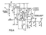
- Figure 4 is a circuit diagram of a circuit according to the invention that produces output currents proportional to an exponential function of a product or a ratio of input currents.
- FIG. 2 is a circuit diagram of a multiple-output square root circuit according to the invention.
- the circuit includes an input diode chain 14 and an output diode chain 18.
- the diodes may be the base-emitter junctions of npn transistors, where the base of each transistor is connected to the transistor's collector.
- Diode chain 14 consists of two input sub-chains 20 and 22, each having N diodes, where N is any number greater than or equal to 1.
- Output diode chain 18 has 2N diodes.
- the voltage at the top of input diode chain 14 equals the voltage at the top of output diode chain 18.
- a voltage driving circuit in the form of a differential amplifier 24 forces the voltage at the bottom of diode chain 18 equal to the voltage at the bottom of diode chain 14, as explained in greater detail below.
- a first input current I in1 passes through the entire length of input diode chain 14, while a second input current I in2 passes only through input subchain 20.
- the current through input subchain 20 is equal to I in1 plus I in2
- the current through input subchain 22 is equal to I in1 .
- the small base current to transistor 26 is negligible compared to the input currents I in1 and I in2 , and can thus be ignored.
- the current sources that produce currents I in1 and I in2 can be npn transistors having a resistor connected between the emitter and ground and having a fixed voltage applied to the base.
- V t k B T/q , where k B is Boltzmann's constant, T is the temperature, and q is the charge of an electron.
- I d is the current through the diode, and I s is the saturation current of the diode.
- I s for each diode is proportional to the diode area.
- I s is typically in the range of 10 ⁇ 18 to 10 ⁇ 16 amperes, and I d » I s , the voltage across each diode closely approximates V t ⁇ ln(I d /I s ) .
- the voltage across diode subchain 20 is therefore NV t ⁇ ln[(I in1 +I in2 )/I s20 ]
- the voltage across input subchain 22 is NV t ⁇ ln(I in1 /I s22 )
- I s20 and I s22 are the saturation currents of each of the diodes in diode subchain 20 and each of the diodes in diode subchain 22, respectively.
- the current I o flows into the collector of transistor 29.
- the actual output currents of the square root circuit, I o1 , and I o2 flow into the collectors of transistors 30 and 32, which have their bases connected to the base of transistor 29.
- Resistors 34, 36, and 38 connect the emitters of transistors 29, 30, and 32, respectively, to ground. If the resistors 34, 36, and 38 all have the same resistance, and if the emitter areas of all three transistors 29, 30, and 32 are the same, then output currents I o1 , and I o2 , which enter the collectors of transistors 30 and 32, respectively, will both be equal to the current I o that enters the collector of transistor 29.
- the output current I o1 will be k times I o .
- the voltage across resistor 36 or resistor 38 is low enough, the voltage at the collector of transistor 30 or transistor 32 can be as low as 0.2 volts without transistors 30 or 32 becoming saturated.
- transistors 30 and 32 provide output current sources that can drive low output voltages.
- Diode chain 12 is used to provide sufficient head room for the proper operation of the input current sources, as described below.
- "Head room” as used in this specification and in the claims refers to the voltages above the input current sources as shown in the Figures, e.g., the voltage at the base of transistor 26 and the voltage at the point between input diode subchains 20 and 22 in Fig. 2.
- Diode chain 16 is used to ensure that transistors 26 and 28 of differential amplifier 24 are not saturated, and to reduce error in the offset voltage V os of differential amplifier 24, as described below.
- Diode chain 16 has M diodes, and diode chain 12 has M+2N+2 diodes.
- the number M can be any number greater than or equal to zero.
- the value of M determines the voltage at the base of transistor 26 and the voltage at the point between input diode subchains 20 and 22, and hence the value of M determines the amount of head room available for the input current sources.
- the voltage at the top of diode chain 12 is equal to (M+2N+2) ⁇ V be , where V be is the voltage across each diode.
- V be is the voltage across each diode.
- the voltage at the emitter of transistor 42 is equal to (M+2N+1)V be , because the voltage drop across the base emitter junction of transistor 42 is V be .
- diode chain 12 sets up a common reference voltage at the top of diode chains 14 and 18, and provides for a voltage at the bottom of input diode chain 14 that leaves sufficient head room for the proper operation of the input current source associated with I in1 .
- Current source 50 causes current to flow from supply voltage 48 through transistor 46 and diode chain 16.
- the voltage at the base of transistor 46 is equal to (M+2)V be plus the voltage across resistor 34, since the voltage across each diode in diode chain 16 and across the base-emitter junctions of transistors 28 and 46 is V be . Since the base of transistor 46 is connected to the bases of transistors 54 and 56, the voltage at the emitter of transistor 54 and the voltage at the emitter of transistor 56 will equal (M+1)V be plus the voltage across resistor 34. Thus, the voltage at the collectors of transistors 26 and 28 will never be less than the voltages at the bases of transistors 26 and 28.
- Transistors 26 and 28 therefore will never be saturated. Moreover, since the voltages at the collectors of transistors 26 and 28 are the same, error in the offset voltage V os of differential amplifier 24 is minimized.
- Differential amplifier 24 consists of transistors 26, 28, 54, and 56, current sources 52 and 58, and compensation capacitor 60.
- Current source 52 delivers current from supply voltage 48 through transistor 54 to the collector of transistor 26.
- Current source 58 produces a current equal to twice the current produced by current source 52, so that a current flows into the collector of transistor 28 that is equal to the current flowing into the collector of transistor 26. Since the current flowing through transistor 26 equals the current flowing through transistor 28, the base-emitter voltage drop of transistor 26 equals the base-emitter voltage drop of transistor 28.
- differential amplifier 24 drives the voltage at the base of transistor 28 approximately equal to the voltage at the base of transistor 26. Because the differential amplifier 24 is a closed-loop system subject to possible oscillation effects, a compensation capacitor 60 is used to stabilize the differential amplifier 24.
- the accuracy of the square root circuit can be enhanced by increasing the number N of diodes in the input diode subchains 20 and 22.
- N the number of diodes in the input diode subchains 20 and 22.
- the circuit can achieve a high degree of precision.
- the differential amplifier 24 consists entirely of npn transistors, the square root circuit exhibits a high-speed response to changes in the input currents I in1 and I in1 .
- FIG. 3 An alternative configuration of input diode chain 14.
- the bottom of input diode subchain 20 is connected to the base of transistor 62, rather than being connected directly to the top of input diode subchain 22.
- the top of diode subchain 22 is connected to the emitter of transistor 62.
- the collector of transistor 62 is connected to the emitter of transistor 42. Ignoring the small base currents to transistors 26 and 62, the current through input subchain 20 is equal to I in1 , and the current through input subchain 22 is equal to I in2 .
- N-1 diodes rather than N diodes, in input diode subchain 22, because the current I in2 passes through the base-emitter junction of transistor 62, which functions as one diode voltage drop.
- the current I o through diode chain 18 will equal (I in1 ⁇ I in2 ) 1/2 .
- Output diode chain 18 includes subchain 64 and subchain 66.
- the top of diode subchain 64 connects with the emitter of transistor 42.
- the bottom of diode subchain 64 connects with the base of transistor 68.
- the collector of transistor 68 connects with the emitter of transistor 42, and the base-emitter junction of transistor 68 forms the first diode drop in diode subchain 66.
- the bottom of subchain 66 connects with the base of transistor 28 of differential amplifier 24.
- An input current I in3 passes through diode subchain 64.
- the voltage across each diode in diode subchain 64 is V t ⁇ ln(I in3 /I s64 ), where I s64 is the saturation current of each of the diodes in subchain 64.
- the voltage across each diode in diode subchain 66 is V t ⁇ ln(I o /I s66 ) , where I s66 is the saturation current of each of the diodes in subchain 66.
- diode subchain 20 has A diodes
- diode subchain 22 has B diodes
- diode subchain 64 has C diodes
- diodes subchain 66 has D diodes
- a ⁇ V t ⁇ ln(I in2 /I s20 ) + B ⁇ V t ⁇ ln(I in1 /I s22 ) C ⁇ V t ⁇ ln(I in3 /I s64 ) + D ⁇ V t ⁇ ln(I o /I s66 ) .
- (I in2 ) A (I in1 ) B /(I s20 ) A (I s22 ) B (I in3 ) C (I o ) D /(I s64 ) C (I s66 ) D .
- I o [(I s64 ) C (I s66 ) D /(I s20 ) A (I s22 ) B ] ⁇ [(I in2 ) A (I in1 ) B /(I in3 ) C ] 1/D .
- I o k[(I in2 ) A (I in1 ) B /(I in3 ) C ] 1/D , where k is a constant.
Landscapes
- Physics & Mathematics (AREA)
- Engineering & Computer Science (AREA)
- Mathematical Physics (AREA)
- Theoretical Computer Science (AREA)
- Software Systems (AREA)
- Computer Hardware Design (AREA)
- General Physics & Mathematics (AREA)
- Amplifiers (AREA)
Applications Claiming Priority (2)
| Application Number | Priority Date | Filing Date | Title |
|---|---|---|---|
| US07/485,059 US5065053A (en) | 1990-02-26 | 1990-02-26 | Exponential function circuitry |
| US485059 | 1995-06-07 |
Publications (3)
| Publication Number | Publication Date |
|---|---|
| EP0444361A2 true EP0444361A2 (fr) | 1991-09-04 |
| EP0444361A3 EP0444361A3 (en) | 1991-12-18 |
| EP0444361B1 EP0444361B1 (fr) | 1999-03-31 |
Family
ID=23926786
Family Applications (1)
| Application Number | Title | Priority Date | Filing Date |
|---|---|---|---|
| EP90314331A Expired - Lifetime EP0444361B1 (fr) | 1990-02-26 | 1990-12-27 | Circuit pour fonction exponentielle |
Country Status (5)
| Country | Link |
|---|---|
| US (1) | US5065053A (fr) |
| EP (1) | EP0444361B1 (fr) |
| JP (1) | JPH0561994A (fr) |
| CA (1) | CA2035296A1 (fr) |
| DE (1) | DE69033030T2 (fr) |
Cited By (2)
| Publication number | Priority date | Publication date | Assignee | Title |
|---|---|---|---|---|
| DE4300591A1 (de) * | 1993-01-13 | 1994-07-14 | Telefunken Microelectron | Schaltungsanordnung |
| WO2002071597A3 (fr) * | 2001-02-12 | 2003-07-17 | Infineon Technologies Ag | Ensemble circuit servant a mettre a disposition une predistorsion exponentielle pour un amplificateur variable |
Families Citing this family (10)
| Publication number | Priority date | Publication date | Assignee | Title |
|---|---|---|---|---|
| US5200655A (en) * | 1991-06-03 | 1993-04-06 | Motorola, Inc. | Temperature-independent exponential converter |
| JP2890381B2 (ja) * | 1991-12-28 | 1999-05-10 | シャープ株式会社 | 対数圧縮回路 |
| US5391947A (en) * | 1992-08-10 | 1995-02-21 | International Business Machines Corporation | Voltage ratio to current circuit |
| US5331289A (en) * | 1993-02-08 | 1994-07-19 | Tektronix, Inc. | Translinear fT multiplier |
| US5428611A (en) * | 1993-05-28 | 1995-06-27 | Digital Equipment Corporation | Strong framing protocol for HDLC and other run-length codes |
| US7387198B2 (en) * | 2003-05-07 | 2008-06-17 | Vibra-Dyn, Llc | Balanced flat stroke bi-directional conveyor |
| US7546332B2 (en) * | 2004-11-09 | 2009-06-09 | Theta Microelectronics, Inc. | Apparatus and methods for implementation of mathematical functions |
| KR100730609B1 (ko) * | 2005-02-01 | 2007-06-21 | 삼성전자주식회사 | 지수 함수 발생 장치 |
| TWI345199B (en) * | 2006-11-03 | 2011-07-11 | Chimei Innolux Corp | Power switch circuit and liquid crystal display using the same |
| KR101774245B1 (ko) | 2013-02-18 | 2017-09-19 | 엘에스산전 주식회사 | Rms 검출기 및 이를 적용한 차단기 |
Family Cites Families (12)
| Publication number | Priority date | Publication date | Assignee | Title |
|---|---|---|---|---|
| US3089968A (en) * | 1961-06-22 | 1963-05-14 | Gen Precision Inc | Non-linear amplifier |
| US3197626A (en) * | 1962-01-08 | 1965-07-27 | Chrysler Corp | Logarithmic multiplier-divider |
| US3417263A (en) * | 1965-03-18 | 1968-12-17 | Ansitron Inc | Logarithmic amplifier |
| US3413456A (en) * | 1965-07-20 | 1968-11-26 | Solartron Electronic Group | Quarter square multiplier |
| US3584232A (en) * | 1969-01-21 | 1971-06-08 | Bell Telephone Labor Inc | Precision logarithmic converter |
| US3599013A (en) * | 1969-02-07 | 1971-08-10 | Bendix Corp | Squaring and square-root-extracting circuits |
| US3668440A (en) * | 1970-10-16 | 1972-06-06 | Motorola Inc | Temperature stable monolithic multiplier circuit |
| US3986048A (en) * | 1973-08-10 | 1976-10-12 | Sony Corporation | Non-linear amplifier |
| US4430626A (en) * | 1979-11-28 | 1984-02-07 | Dbx, Inc. | Networks for the log domain |
| JPS57164609A (en) * | 1981-04-02 | 1982-10-09 | Sony Corp | Level detecting circuit |
| DE3124289A1 (de) * | 1981-06-19 | 1983-01-05 | Licentia Patent-Verwaltungs-Gmbh, 6000 Frankfurt | Schaltungsanordnung zur erzeugung einer von einer wechselspannung abhaengigen steuergleichspannung |
| DE3534808A1 (de) * | 1985-09-30 | 1987-04-02 | Leitz Ernst Gmbh | Schaltungsanordnung zur verringerung der einschwingzeit |
-
1990
- 1990-02-26 US US07/485,059 patent/US5065053A/en not_active Expired - Lifetime
- 1990-12-27 EP EP90314331A patent/EP0444361B1/fr not_active Expired - Lifetime
- 1990-12-27 DE DE69033030T patent/DE69033030T2/de not_active Expired - Fee Related
-
1991
- 1991-01-30 CA CA002035296A patent/CA2035296A1/fr not_active Abandoned
- 1991-02-25 JP JP3029979A patent/JPH0561994A/ja active Pending
Cited By (3)
| Publication number | Priority date | Publication date | Assignee | Title |
|---|---|---|---|---|
| DE4300591A1 (de) * | 1993-01-13 | 1994-07-14 | Telefunken Microelectron | Schaltungsanordnung |
| WO2002071597A3 (fr) * | 2001-02-12 | 2003-07-17 | Infineon Technologies Ag | Ensemble circuit servant a mettre a disposition une predistorsion exponentielle pour un amplificateur variable |
| US6788145B2 (en) | 2001-02-12 | 2004-09-07 | Infineon Technologies Ag | Circuit configuration for producing exponential predistortion for a variable amplifier |
Also Published As
| Publication number | Publication date |
|---|---|
| DE69033030T2 (de) | 1999-11-11 |
| CA2035296A1 (fr) | 1991-08-27 |
| EP0444361B1 (fr) | 1999-03-31 |
| JPH0561994A (ja) | 1993-03-12 |
| DE69033030D1 (de) | 1999-05-06 |
| US5065053A (en) | 1991-11-12 |
| EP0444361A3 (en) | 1991-12-18 |
Similar Documents
| Publication | Publication Date | Title |
|---|---|---|
| US4604532A (en) | Temperature compensated logarithmic circuit | |
| EP0444361A2 (fr) | Circuit pour fonction exponentielle | |
| US4456887A (en) | Differential amplifier | |
| US4528496A (en) | Current supply for use in low voltage IC devices | |
| EP0055573A1 (fr) | Circuit comparateur | |
| US5521544A (en) | Multiplier circuit having circuit wide dynamic range with reduced supply voltage requirements | |
| EP0219682A2 (fr) | Circuit convertisseur de courant en tension | |
| US3304419A (en) | Solid-state analog multiplier circuit | |
| US4885547A (en) | Gain cell with digital control | |
| US4157493A (en) | Delta VBE generator circuit | |
| US3668440A (en) | Temperature stable monolithic multiplier circuit | |
| US3909628A (en) | Voltage-to-current converter and function generator | |
| EP0490016B1 (fr) | Circuit intégré pour engendrer un courant indépendant de la température, proportionnel à la différence de tension entre un signal et une tension de référence | |
| EP0116398B1 (fr) | Circuit de compensation gamma | |
| JPH05506140A (ja) | 指数的な利得制御を行う増幅回路 | |
| US4329598A (en) | Bias generator | |
| EP0061705B1 (fr) | Circuit pour source de courant de faible valeur | |
| EP0110720B1 (fr) | Circuit à miroir de courant | |
| EP0481277B1 (fr) | Source de courant | |
| JP2906461B2 (ja) | 温度センサ回路 | |
| JP3022594B2 (ja) | 調整可能な遅延を有する遅延回路 | |
| JPS5986316A (ja) | 差動増幅器対の切替回路 | |
| US5391947A (en) | Voltage ratio to current circuit | |
| US4859966A (en) | Current amplifier circuit and a current amplifying type differential current converter circuit | |
| JPH0716151B2 (ja) | 波形整形回路 |
Legal Events
| Date | Code | Title | Description |
|---|---|---|---|
| PUAI | Public reference made under article 153(3) epc to a published international application that has entered the european phase |
Free format text: ORIGINAL CODE: 0009012 |
|
| 17P | Request for examination filed |
Effective date: 19910102 |
|
| AK | Designated contracting states |
Kind code of ref document: A2 Designated state(s): DE FR GB IT |
|
| PUAL | Search report despatched |
Free format text: ORIGINAL CODE: 0009013 |
|
| AK | Designated contracting states |
Kind code of ref document: A3 Designated state(s): DE FR GB IT |
|
| 17Q | First examination report despatched |
Effective date: 19961125 |
|
| RAP1 | Party data changed (applicant data changed or rights of an application transferred) |
Owner name: QUANTUM CORPORATION |
|
| GRAG | Despatch of communication of intention to grant |
Free format text: ORIGINAL CODE: EPIDOS AGRA |
|
| GRAG | Despatch of communication of intention to grant |
Free format text: ORIGINAL CODE: EPIDOS AGRA |
|
| GRAH | Despatch of communication of intention to grant a patent |
Free format text: ORIGINAL CODE: EPIDOS IGRA |
|
| GRAH | Despatch of communication of intention to grant a patent |
Free format text: ORIGINAL CODE: EPIDOS IGRA |
|
| GRAA | (expected) grant |
Free format text: ORIGINAL CODE: 0009210 |
|
| AK | Designated contracting states |
Kind code of ref document: B1 Designated state(s): DE FR GB IT |
|
| REF | Corresponds to: |
Ref document number: 69033030 Country of ref document: DE Date of ref document: 19990506 |
|
| ET | Fr: translation filed | ||
| PLBE | No opposition filed within time limit |
Free format text: ORIGINAL CODE: 0009261 |
|
| STAA | Information on the status of an ep patent application or granted ep patent |
Free format text: STATUS: NO OPPOSITION FILED WITHIN TIME LIMIT |
|
| 26N | No opposition filed | ||
| PG25 | Lapsed in a contracting state [announced via postgrant information from national office to epo] |
Ref country code: FR Free format text: LAPSE BECAUSE OF NON-PAYMENT OF DUE FEES Effective date: 20000831 |
|
| REG | Reference to a national code |
Ref country code: FR Ref legal event code: ST |
|
| PGFP | Annual fee paid to national office [announced via postgrant information from national office to epo] |
Ref country code: GB Payment date: 20001201 Year of fee payment: 11 |
|
| PGFP | Annual fee paid to national office [announced via postgrant information from national office to epo] |
Ref country code: DE Payment date: 20001211 Year of fee payment: 11 |
|
| PG25 | Lapsed in a contracting state [announced via postgrant information from national office to epo] |
Ref country code: GB Free format text: LAPSE BECAUSE OF NON-PAYMENT OF DUE FEES Effective date: 20011227 |
|
| REG | Reference to a national code |
Ref country code: GB Ref legal event code: IF02 |
|
| PG25 | Lapsed in a contracting state [announced via postgrant information from national office to epo] |
Ref country code: DE Free format text: LAPSE BECAUSE OF NON-PAYMENT OF DUE FEES Effective date: 20020702 |
|
| GBPC | Gb: european patent ceased through non-payment of renewal fee |
Effective date: 20011227 |
|
| PG25 | Lapsed in a contracting state [announced via postgrant information from national office to epo] |
Ref country code: IT Free format text: LAPSE BECAUSE OF NON-PAYMENT OF DUE FEES;WARNING: LAPSES OF ITALIAN PATENTS WITH EFFECTIVE DATE BEFORE 2007 MAY HAVE OCCURRED AT ANY TIME BEFORE 2007. THE CORRECT EFFECTIVE DATE MAY BE DIFFERENT FROM THE ONE RECORDED. Effective date: 20051227 |