EP0444826A2 - Circuit de protection pour un dispositif semi-conducteur - Google Patents
Circuit de protection pour un dispositif semi-conducteur Download PDFInfo
- Publication number
- EP0444826A2 EP0444826A2 EP91301408A EP91301408A EP0444826A2 EP 0444826 A2 EP0444826 A2 EP 0444826A2 EP 91301408 A EP91301408 A EP 91301408A EP 91301408 A EP91301408 A EP 91301408A EP 0444826 A2 EP0444826 A2 EP 0444826A2
- Authority
- EP
- European Patent Office
- Prior art keywords
- circuit
- switching device
- power switching
- main
- circuits
- Prior art date
- Legal status (The legal status is an assumption and is not a legal conclusion. Google has not performed a legal analysis and makes no representation as to the accuracy of the status listed.)
- Granted
Links
Images




Classifications
-
- H—ELECTRICITY
- H02—GENERATION; CONVERSION OR DISTRIBUTION OF ELECTRIC POWER
- H02H—EMERGENCY PROTECTIVE CIRCUIT ARRANGEMENTS
- H02H9/00—Emergency protective circuit arrangements for limiting excess current or voltage without disconnection
- H02H9/02—Emergency protective circuit arrangements for limiting excess current or voltage without disconnection responsive to excess current
-
- H—ELECTRICITY
- H02—GENERATION; CONVERSION OR DISTRIBUTION OF ELECTRIC POWER
- H02H—EMERGENCY PROTECTIVE CIRCUIT ARRANGEMENTS
- H02H5/00—Emergency protective circuit arrangements for automatic disconnection directly responsive to an undesired change from normal non-electric working conditions with or without subsequent reconnection
- H02H5/04—Emergency protective circuit arrangements for automatic disconnection directly responsive to an undesired change from normal non-electric working conditions with or without subsequent reconnection responsive to abnormal temperature
- H02H5/041—Emergency protective circuit arrangements for automatic disconnection directly responsive to an undesired change from normal non-electric working conditions with or without subsequent reconnection responsive to abnormal temperature additionally responsive to excess current
Definitions
- the present invention relates to an overcurrent protection circuit for a semiconductor device for an inverter, and more particularly to a protection circuit whose composition may be simplified and whose number of circuit components may be reduced.
- a base driving circuit for a power transistor used as a power switching device indicates a pair of NPN power transistors in Darlington connection
- DR indicates a base drive circuit
- the numeral 3 designates a power supply of this base driving circuit (a driving power supply).
- the reference characters Si1 and Si2 are referred to input terminals of a driving signal S which turns on and off the power transistor TR.
- the power transistor TR turns on when a photo-coupler PC1 turns on, and similarly the power transistor TR turns off when the photo-coupler PC1 turns off.
- Figure 8 shows an example of an inverter circuit which comprises the base driving circuits as shown in Figure 9 and the power transistors.
- TR1 to TR6 are NPN power transistors which are connected in bridge to form a three phase inverter, and IM denotes an induction motor.
- IM denotes an induction motor.
- DC electric power applied between a positive line (+) LP and a negative line (-) LN of main DC electrodes is converted into three-phase AC electric power.
- the three phases, U, V, W, are supplied to the induction motor IM from each connection point (a midpoint) between the upper and lower arms of the bridge.
- the base driving circuit DR as shown in Figure 9 When the base driving circuit DR as shown in Figure 9 is used in the inverter as shown in Figure 8, it requires three insulated driving power supplies 3 each corresponding to a respective one of the transistors TR1, TR3 and TR5, because they are in the upper arms and the negative electrodes of these driving power supplies 3 are each coupled to different output lines of the three phase which differ in electrical potential from each other.
- the driving power supplies 3 in an inverter circuit in three phase bridge connection may consist of at least four power supplies, three for the upper arms and one for the lower arms.
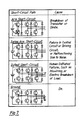
- short-circuit faults may occur such as an arm short-circuit, a series arm short-circuit, an output short-circuit or a ground. These are illustrated schematically in Figure 7.
- the power transistor TR When these faults occur, an overcurrent flows through the power transistor TR.
- the power transistor has a Over Load Safe Operation Area (OLSOA) in its collector current I CP versus collector-emitter voltage V CE characteristic diagram as shown in Figure 6 and will not fail until the locus of I CP deviates from the OLSOA. Then, at a short-circuit fault the power transistors must be instantly brought into turn-off mode by detecting overcurrent by means of the circuit as shown in Figure 5.
- OSOA Over Load Safe Operation Area
- Figure 5 shows a schematic diagram of the base driving circuit with a function of overcurrent protection.
- the part enclosed by a broken line is an overcurrent protection circuit OC.
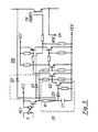
- Figure 3 shows a particular example of a circuit composition of the base driving (in this case, gate driving) circuit with overcurrent protecting function using an IGBT as a power switching device which is equivalent to the power transistor TR in Figure 5.
- the part enclosed with a broken line is also an overcurrent protection circuit OC, and the other part is a base driving circuit DR.
- the basic function of the circuit in Figure 3 is the same as that in Figure 5, but the driving signal S is given through a photo-coupler PC1 as is the case in Figure 9, and the base driving circuit DR is more complex.
- an alarm signal ALM is applied to a driving signal generating circuit for cutting the driving signal S, which further turns off simultaneously six power device elements in a three phase inverter circuit to protect these power switching devices even if an overcurrent flows through only one of the chips of these power device elements.
- the conventional overcurrent protection circuit described above has the problems now to be enumerated.
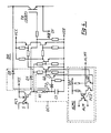
- the driving circuit with alarm circuit in Figure 4 is used in a three phase inverter circuit such as is seen in Figure 8, the lines for alarm signals ALM for each power transistor must be insulated from each other for being collected together in order to supply the signals to an apparatus (a microcomputer, for example) which controls the driving signals for the six transistor elements, because the electrical potentials of the driving power supplies 3 are different from each other for each of transistors TR1, TR3 and TR5 in the upper three arms and for all of transistors TR2, TR4 and TR6 in the lower three arms. Consequently, at least four photo-couplers in total, indicated as PC2 in Figure 4, are needed to provide an alarm function in the inverter circuit. This causes complexity of the circuit with the need for an increased number of components.
- the present invention aims to solve the above problems and to provide a simplified protection circuit for a semiconductor device that permits the use of electronic components capable only of withstanding low voltages, thus reducing cost.
- Overheating due to an overcurrent state is detected for power switching devices being at least in the upper arms of a bridged inverter circuit in Figure 8 by means of temperature sensors such as thermistors disposed in proximity to these devices through transmission lines electrically insulated from the devices.
- Figure 1 shows a schematic circuit as an example of the embodiments of the present invention.
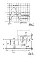
- Figure 2 shows respective wave forms of a base current I B , a collector current I C and a collector-emitter voltage V CE of the power transistor during the overcurrent protection by the circuits in Figure 3 to Figure 5.
- respective power transistors TR1 to TR6, which constitute an inverter circuit in a three phase bridge connection are in this case power transistor chips, and these six chips are to be contained in one package.
- the overcurrent protection circuits OC for the power transistors TR1, TR3 and TR5 in the upper arms of the bridge, and a base driving circuit DR are the same as those in Figure 3 which do not emit alarm signals.
- the overcurrent protection circuits for the power transistors TR2, TR4 and TR6 in the lower arms of the bridge are those which emit alarm signals ALM1, and the overcurrent protection circuit with alarm circuit OC1 seen in Figure 4 may be used for them without any modification.
- This alarm signal ALM1 may be taken out directly from the alarm circuit without being relayed through a photo-coupler PC2, for example, from the collector of a transistor Q3 in the previous stage, because each emitter of these three power transistors TR2, TR4 and TR6 is coupled together to the negative line (-) LN of a main DC power supply which is on a point of reference potential. Then, in the present invention, the alarm photo-coupler PC2 may be eliminated from the overcurrent protection circuit with alarm circuit OC1 in Figure 4. These three alarm signals ALM1 are lead to the OR circuit G1. In the lower arms, the base driving circuits DR for the power transistors TR2, TR4 and TR6 are the same as those shown in Figure 3 or Figure 4.
- Temperature sensors H such as thermistors are disposed in proximity to the chips or elements of the power transistors TR1, TR3 and TR5. Each temperature sensor H is coupled to the OR circuit G1 through the overheat protection circuit OH whose negative line is equipotentially coupled to the negative line (-) LN of the main DC power supply on the point of reference potential.
- the latching of the overcurrent protection circuit OC is then released when the pulsed driving signal S, which is given as an input signal to the base driving circuit DR of the transistor element, becomes OFF mode, since the capacitor C1 is not charged through the resistor R1 but discharges its charge through Q2 to reduce the terminal voltage below the avalanche voltage of the zener diode ZD to turn off Q2.
- I C and V CE of the power transistor element have the same waveforms in Figure 2 again to reheat the power transistor element.
- any of the elements TR1, TR3 and TR5, through which the overcurrent flows, are overheated, and when the temperature of the overheated element exceeds a predetermined value, the overheat protection circuit OH functions to give an alarm signal ALM2 to the OR circuit G1.
- the alarm signals due to overcurrent in any of the six power transistors TR1 to TR6 are given to the OR circuit G1.
- the output of this OR circuit G1, an alarm signal ALM0 is then given to a microcomputer not shown in the figure.
- the microcomputer gives the overcurrent protection circuits the driving signals S in OFF mode, which are transmitted to the six transistors through photo-couplers by signal transmission lines which are insulated from the main circuits.
- the six transistors TR1 to TR6 are then turned off simultaneously, and are thus protected.
- power transistors are used as switching devices, however, the switching devices are not limited to the power transistors but any switching devices of the self-turn-off type may be applicable to the present invention.
- the number of the temperature sensors H may be less than that of the power transistors. At least two sensors H may be provided, accomplishing their purpose of overcurrent protection if the power transistors TR1, TR3 and TR5 are disposed in close proximity to allow the temperature sensors to be disposed among them so that overheating of any one of the power transistors TR1, TR3 or TR5 will be detected by the sensor.
- the overcurrent protection circuits OC1 for the power transistors TR2, TR4 and TR6 in the lower arms of the bridge are provided for each power transistor element, but the purpose of the present invention may also be accomplished by, for example, coupling the emitters of the three power transistors TR2, TR4 and TR6 together to a terminal, inserting a shunt resistor between this terminal and the negative line (-) LN of main DC power supply, detecting increase of potential difference between both ends of this shunt resistor and transmitting this increase to only one overcurrent protection circuit which simultaneously turns off the three elements in the lower arms of the bridge to achieve the overcurrent protection.
- Another embodiment that may also be applied to the present invention is that which detects any of the V CE (sat) of the power transistors TR2, TR4 and TR6 exceeding a normal value by an overcurrent protection circuit which has three diodes D2 each coupled in parallel to the collectors of these three elements and effects overcurrent protection by turning them off simultaneously.
- OR circuits may also be applied without departing from the scope of the present invention, one of which OR circuits receives the alarm signals ALM1 from the overcurrent protection circuits OC for the power transistors in the lower three arms, and the other OR circuit receiving the alarm signal ALM2 from the overheating protection circuit OH.
- the temperature sensors H are not always necessarily contained in the same package with TR1, TR3 and TR5, but may be disposed outside the package if these sensors are in positions that enable them effectively to detect overheating of TR1, TR3 and TR5.
Landscapes
- Engineering & Computer Science (AREA)
- Power Engineering (AREA)
- Inverter Devices (AREA)
- Electronic Switches (AREA)
- Protection Of Static Devices (AREA)
Applications Claiming Priority (2)
| Application Number | Priority Date | Filing Date | Title |
|---|---|---|---|
| JP45016/90 | 1990-02-26 | ||
| JP2045016A JP2811872B2 (ja) | 1990-02-26 | 1990-02-26 | 半導体装置の保護回路 |
Publications (3)
| Publication Number | Publication Date |
|---|---|
| EP0444826A2 true EP0444826A2 (fr) | 1991-09-04 |
| EP0444826A3 EP0444826A3 (en) | 1992-12-16 |
| EP0444826B1 EP0444826B1 (fr) | 1996-10-02 |
Family
ID=12707558
Family Applications (1)
| Application Number | Title | Priority Date | Filing Date |
|---|---|---|---|
| EP91301408A Expired - Lifetime EP0444826B1 (fr) | 1990-02-26 | 1991-02-21 | Circuit de protection pour un dispositif semi-conducteur |
Country Status (5)
| Country | Link |
|---|---|
| US (1) | US5115388A (fr) |
| EP (1) | EP0444826B1 (fr) |
| JP (1) | JP2811872B2 (fr) |
| KR (1) | KR0122309B1 (fr) |
| DE (1) | DE69122419T2 (fr) |
Cited By (8)
| Publication number | Priority date | Publication date | Assignee | Title |
|---|---|---|---|---|
| WO2004107550A1 (fr) | 2003-05-28 | 2004-12-09 | Abb Oy | Surveillance de la temperature de modules onduleurs montes en parallele |
| EP1056205A3 (fr) * | 1999-05-27 | 2005-01-19 | Fuji Electric Co. Ltd. | Dispositif semiconducteur |
| US6999329B2 (en) | 2003-04-25 | 2006-02-14 | Abb Oy | Temperature monitoring of parallel-connected inverter modules |
| EP1646120A3 (fr) * | 2002-08-22 | 2006-07-12 | ABB Oy | Procédé en relation avec une inductance de sortie d'un invertisseur |
| EP1868273A3 (fr) * | 2006-05-23 | 2009-09-23 | HanBit Tech Inc. | Déclencheur automatique, système de réseau qui l'utilise et procédé de contrôle de celui-ci |
| US7836365B2 (en) | 2002-03-01 | 2010-11-16 | Broadcom Corporation | System and method for testing a circuit |
| CN102299507A (zh) * | 2010-06-28 | 2011-12-28 | 富士电机株式会社 | 用于半导体元件的驱动装置 |
| EP2560283A4 (fr) * | 2010-04-14 | 2013-09-04 | Honda Motor Co Ltd | Procédé de protection contre les courts-circuits |
Families Citing this family (25)
| Publication number | Priority date | Publication date | Assignee | Title |
|---|---|---|---|---|
| JPH04285465A (ja) * | 1991-03-13 | 1992-10-09 | Nec Corp | 保護回路付スイッチング電源 |
| DE69314898T2 (de) * | 1992-08-28 | 1998-05-28 | Sgs Thomson Microelectronics | Übertemperaturwarnzyklus beim Betrieb eines mehrphasigen Gleichstrommotors |
| DE19920505B4 (de) * | 1999-05-05 | 2004-05-27 | Semikron Elektronik Gmbh | Umrichter mit Temperatursymmetrierung |
| US6934139B2 (en) * | 2000-05-01 | 2005-08-23 | Fuji Electric Device Technology Co., Ltd. | Intelligent power module |
| DE10302811A1 (de) * | 2003-01-24 | 2004-08-12 | Siemens Ag | Schaltungsanordnung zum Schutz einer Leistungsendstufe mit Halbleiterschaltern |
| FI116175B (fi) * | 2003-12-19 | 2005-09-30 | Abb Oy | Menetelmä ja järjestely taajuusmuuttajan suojaamiseksi |
| US7110272B2 (en) * | 2004-06-22 | 2006-09-19 | Smc Electrical Products, Inc. | Inverter bridge controller implementing short-circuit protection scheme |
| JP2006280193A (ja) * | 2005-03-03 | 2006-10-12 | Toyota Motor Corp | 駆動回路の異常判定装置およびこれを備える駆動装置並びに駆動回路の異常判定方法 |
| JP4654940B2 (ja) * | 2006-02-27 | 2011-03-23 | 株式会社デンソー | インバータ装置及びインバータ回路の駆動制御方法 |
| US8014118B2 (en) | 2007-02-27 | 2011-09-06 | Fuji Electric Systems Co., Ltd. | Load driving circuit, driver IC having a load driving circuit, and plasma display panel having a driver IC |
| CN101937888B (zh) * | 2009-07-01 | 2013-01-23 | 辉达公司 | 用于控制电路板上多个单元散热的电路、系统及方法 |
| US20110018488A1 (en) * | 2009-07-22 | 2011-01-27 | Chia-Hsuan Lin | Frequency-changing control apparatus |
| TWI413358B (zh) * | 2009-09-18 | 2013-10-21 | Sunonwealth Electr Mach Ind Co | Used for fan control systems |
| JP5724730B2 (ja) | 2010-12-14 | 2015-05-27 | 富士電機株式会社 | 半導体素子の駆動装置 |
| CN103460588B (zh) * | 2011-04-08 | 2016-05-25 | 富士电机株式会社 | 电力转换装置的控制装置 |
| DE102011076907B4 (de) * | 2011-06-01 | 2024-06-06 | Robert Bosch Gmbh | Verfahren zum Betreiben eines Wechselrichters sowie Wechselrichter |
| DE102011076908A1 (de) * | 2011-06-01 | 2012-12-06 | Robert Bosch Gmbh | Verfahren zum Betreiben eines Wechselrichters sowie Wechselrichter |
| JP2013220708A (ja) * | 2012-04-16 | 2013-10-28 | Mitsubishi Heavy Ind Ltd | 熱媒体加熱装置およびそれを備えた車両用空調装置 |
| CN103809708A (zh) | 2012-11-07 | 2014-05-21 | 辉达公司 | 平板电子设备及其辅助散热装置、以及两者的组件 |
| KR101412914B1 (ko) * | 2012-11-22 | 2014-06-26 | 삼성전기주식회사 | 과열 보호 회로 |
| US9673007B2 (en) | 2013-09-20 | 2017-06-06 | Maxim Integrated Products, Inc. | Systems and methods for discharging inductors with temperature protection |
| DE102014112760A1 (de) | 2013-09-20 | 2015-03-26 | Maxim Integrated Products, Inc. | Systeme und Verfahren zum Entladen von Induktivitäten mit Temperaturschutz |
| US20170030962A1 (en) * | 2015-07-27 | 2017-02-02 | Hyundai Motor Company | Circuit for detecting failure of insulated gate bipolar transistor (igbt) power module |
| JP6398949B2 (ja) * | 2015-11-05 | 2018-10-03 | 三菱電機株式会社 | 半導体素子の駆動装置 |
| JP7600565B2 (ja) * | 2020-08-25 | 2024-12-17 | 富士電機株式会社 | 半導体装置 |
Family Cites Families (11)
| Publication number | Priority date | Publication date | Assignee | Title |
|---|---|---|---|---|
| FR2252682A1 (en) * | 1973-11-22 | 1975-06-20 | Simplex Appareils | Electronic circuit-breaker for transformer - thermocouple and resistor detect large and small overloads |
| DD134705A1 (de) * | 1977-12-23 | 1979-03-14 | Wigand Gunther | Schutzschaltungsanordnung fuer elektrische leistungsscha |
| DE2803557A1 (de) * | 1978-01-27 | 1979-08-02 | Bosch Gmbh Robert | Abschaltvorrichtung fuer ein steuerbares halbleiterelement |
| JPS5928152B2 (ja) * | 1978-11-04 | 1984-07-11 | ファナック株式会社 | 電動機駆動用インバ−タ回路の保護装置 |
| DD155275A1 (de) * | 1980-12-15 | 1982-05-26 | Norbert Blacha | Schutzschaltung fuer halbleiterwechselrichter |
| US4360852A (en) * | 1981-04-01 | 1982-11-23 | Allis-Chalmers Corporation | Overcurrent and overtemperature protective circuit for power transistor system |
| JPS60121991A (ja) * | 1983-12-02 | 1985-06-29 | Mitsubishi Electric Corp | インバ−タ制御空気調和装置 |
| JPH0787247B2 (ja) * | 1988-05-27 | 1995-09-20 | 三菱電機株式会社 | 半導体装置 |
| GB2221806B (en) * | 1988-06-27 | 1992-08-12 | Eaton Corp | Inverter short circuit protection method and apparatus |
| US4866559A (en) * | 1988-07-26 | 1989-09-12 | Texas Instruments Incorporated | Solid state circuit protector |
| US4965710A (en) * | 1989-11-16 | 1990-10-23 | International Rectifier Corporation | Insulated gate bipolar transistor power module |
-
1990
- 1990-02-26 JP JP2045016A patent/JP2811872B2/ja not_active Expired - Fee Related
-
1991
- 1991-02-21 DE DE69122419T patent/DE69122419T2/de not_active Expired - Fee Related
- 1991-02-21 EP EP91301408A patent/EP0444826B1/fr not_active Expired - Lifetime
- 1991-02-26 US US07/661,513 patent/US5115388A/en not_active Expired - Lifetime
- 1991-02-26 KR KR1019910003057A patent/KR0122309B1/ko not_active Expired - Fee Related
Cited By (10)
| Publication number | Priority date | Publication date | Assignee | Title |
|---|---|---|---|---|
| EP1056205A3 (fr) * | 1999-05-27 | 2005-01-19 | Fuji Electric Co. Ltd. | Dispositif semiconducteur |
| US7836365B2 (en) | 2002-03-01 | 2010-11-16 | Broadcom Corporation | System and method for testing a circuit |
| EP1646120A3 (fr) * | 2002-08-22 | 2006-07-12 | ABB Oy | Procédé en relation avec une inductance de sortie d'un invertisseur |
| US6999329B2 (en) | 2003-04-25 | 2006-02-14 | Abb Oy | Temperature monitoring of parallel-connected inverter modules |
| WO2004107550A1 (fr) | 2003-05-28 | 2004-12-09 | Abb Oy | Surveillance de la temperature de modules onduleurs montes en parallele |
| CN100472932C (zh) * | 2003-05-28 | 2009-03-25 | Abb有限公司 | 并联逆变器模块的温度监测方法和装置 |
| EP1868273A3 (fr) * | 2006-05-23 | 2009-09-23 | HanBit Tech Inc. | Déclencheur automatique, système de réseau qui l'utilise et procédé de contrôle de celui-ci |
| EP2560283A4 (fr) * | 2010-04-14 | 2013-09-04 | Honda Motor Co Ltd | Procédé de protection contre les courts-circuits |
| CN102299507A (zh) * | 2010-06-28 | 2011-12-28 | 富士电机株式会社 | 用于半导体元件的驱动装置 |
| CN102299507B (zh) * | 2010-06-28 | 2015-05-27 | 富士电机株式会社 | 用于半导体元件的驱动装置 |
Also Published As
| Publication number | Publication date |
|---|---|
| US5115388A (en) | 1992-05-19 |
| JPH03247114A (ja) | 1991-11-05 |
| KR920000166A (ko) | 1992-01-10 |
| EP0444826A3 (en) | 1992-12-16 |
| EP0444826B1 (fr) | 1996-10-02 |
| KR0122309B1 (ko) | 1997-11-22 |
| DE69122419D1 (de) | 1996-11-07 |
| DE69122419T2 (de) | 1997-03-06 |
| JP2811872B2 (ja) | 1998-10-15 |
Similar Documents
| Publication | Publication Date | Title |
|---|---|---|
| EP0444826B1 (fr) | Circuit de protection pour un dispositif semi-conducteur | |
| EP0680147B1 (fr) | Module de puissance et dispositif convertisseur de puissance à semi-conducteurs | |
| US5280228A (en) | Inverter circuit | |
| US5200878A (en) | Drive circuit for current sense igbt | |
| EP0664595B1 (fr) | Commande pour semi-conducteur de puissance et commande d'entraínement pour moteur | |
| US5383082A (en) | Overcurrent protector for power element | |
| EP0354435B1 (fr) | Circuit d'attaque pour transistor à grille isolée; et son utilisation dans un circuit de commutation, dans un dispositif de commutation de courant, et dans un système à moteur à induction | |
| EP0814564A1 (fr) | Circuit de commutation électronique avec réduction des transitoires de commutation | |
| US7538587B2 (en) | Power semiconductor device | |
| EP0369448A2 (fr) | Circuit d'attaque utilisable pour dispositif semi-conducteur commandé en tension | |
| EP0431492A2 (fr) | Convertisseur de puissance de type pont avec rendement amélioré | |
| US5365397A (en) | Device for protecting power semiconductor device against short circuit | |
| KR19980071760A (ko) | Igbt의 단락 용량 증진용 회로 및 방법 | |
| JPS63501119A (ja) | モータ制御回路の短絡を感知するための方法及び装置 | |
| KR100436352B1 (ko) | 전력용 반도체장치 | |
| US5737200A (en) | Semiconductor device protection method | |
| US5764466A (en) | Circuit for short circuit detection through resistive shunt in power circuits using unipolar control voltage | |
| US4945358A (en) | Short circuit protection arrangement for a driver circuit | |
| KR0133530B1 (ko) | 구동회로 | |
| JPH08265121A (ja) | 電力用トランジスタの過電流制限回路 | |
| US5216349A (en) | Driving circuit for a switching element including an improved power supply arrangement | |
| JP2002247865A (ja) | 交流チョッパ装置 | |
| US4755923A (en) | Regulated high-voltage power supply | |
| JP3713795B2 (ja) | 制御装置の出力回路 | |
| US4731550A (en) | Circuit having a feed circuit for supplying current to a load resistor |
Legal Events
| Date | Code | Title | Description |
|---|---|---|---|
| PUAI | Public reference made under article 153(3) epc to a published international application that has entered the european phase |
Free format text: ORIGINAL CODE: 0009012 |
|
| AK | Designated contracting states |
Kind code of ref document: A2 Designated state(s): DE FR GB |
|
| PUAL | Search report despatched |
Free format text: ORIGINAL CODE: 0009013 |
|
| AK | Designated contracting states |
Kind code of ref document: A3 Designated state(s): DE FR GB |
|
| 17P | Request for examination filed |
Effective date: 19930220 |
|
| 17Q | First examination report despatched |
Effective date: 19940214 |
|
| GRAG | Despatch of communication of intention to grant |
Free format text: ORIGINAL CODE: EPIDOS AGRA |
|
| GRAH | Despatch of communication of intention to grant a patent |
Free format text: ORIGINAL CODE: EPIDOS IGRA |
|
| GRAH | Despatch of communication of intention to grant a patent |
Free format text: ORIGINAL CODE: EPIDOS IGRA |
|
| GRAA | (expected) grant |
Free format text: ORIGINAL CODE: 0009210 |
|
| AK | Designated contracting states |
Kind code of ref document: B1 Designated state(s): DE FR GB |
|
| REF | Corresponds to: |
Ref document number: 69122419 Country of ref document: DE Date of ref document: 19961107 |
|
| ET | Fr: translation filed | ||
| PLBE | No opposition filed within time limit |
Free format text: ORIGINAL CODE: 0009261 |
|
| STAA | Information on the status of an ep patent application or granted ep patent |
Free format text: STATUS: NO OPPOSITION FILED WITHIN TIME LIMIT |
|
| 26N | No opposition filed | ||
| PGFP | Annual fee paid to national office [announced via postgrant information from national office to epo] |
Ref country code: DE Payment date: 19991231 Year of fee payment: 10 |
|
| PGFP | Annual fee paid to national office [announced via postgrant information from national office to epo] |
Ref country code: FR Payment date: 20000210 Year of fee payment: 10 |
|
| PGFP | Annual fee paid to national office [announced via postgrant information from national office to epo] |
Ref country code: GB Payment date: 20000216 Year of fee payment: 10 |
|
| PG25 | Lapsed in a contracting state [announced via postgrant information from national office to epo] |
Ref country code: GB Free format text: LAPSE BECAUSE OF NON-PAYMENT OF DUE FEES Effective date: 20010221 |
|
| GBPC | Gb: european patent ceased through non-payment of renewal fee |
Effective date: 20010221 |
|
| PG25 | Lapsed in a contracting state [announced via postgrant information from national office to epo] |
Ref country code: FR Free format text: LAPSE BECAUSE OF NON-PAYMENT OF DUE FEES Effective date: 20011031 |
|
| REG | Reference to a national code |
Ref country code: FR Ref legal event code: ST |
|
| PG25 | Lapsed in a contracting state [announced via postgrant information from national office to epo] |
Ref country code: DE Free format text: LAPSE BECAUSE OF NON-PAYMENT OF DUE FEES Effective date: 20011201 |