EP0444843A2 - Capteurs interférentiels et méthodes pour mesurer une grandeur physique utilisant tel capteurs aussi bien que système de contrôle d'un véhicule - Google Patents
Capteurs interférentiels et méthodes pour mesurer une grandeur physique utilisant tel capteurs aussi bien que système de contrôle d'un véhicule Download PDFInfo
- Publication number
- EP0444843A2 EP0444843A2 EP91301479A EP91301479A EP0444843A2 EP 0444843 A2 EP0444843 A2 EP 0444843A2 EP 91301479 A EP91301479 A EP 91301479A EP 91301479 A EP91301479 A EP 91301479A EP 0444843 A2 EP0444843 A2 EP 0444843A2
- Authority
- EP
- European Patent Office
- Prior art keywords
- frequency
- interference
- signal
- electronic
- modulation
- Prior art date
- Legal status (The legal status is an assumption and is not a legal conclusion. Google has not performed a legal analysis and makes no representation as to the accuracy of the status listed.)
- Granted
Links
Images








Classifications
-
- G—PHYSICS
- G01—MEASURING; TESTING
- G01C—MEASURING DISTANCES, LEVELS OR BEARINGS; SURVEYING; NAVIGATION; GYROSCOPIC INSTRUMENTS; PHOTOGRAMMETRY OR VIDEOGRAMMETRY
- G01C19/00—Gyroscopes; Turn-sensitive devices using vibrating masses; Turn-sensitive devices without moving masses; Measuring angular rate using gyroscopic effects
- G01C19/58—Turn-sensitive devices without moving masses
- G01C19/64—Gyrometers using the Sagnac effect, i.e. rotation-induced shifts between counter-rotating electromagnetic beams
- G01C19/72—Gyrometers using the Sagnac effect, i.e. rotation-induced shifts between counter-rotating electromagnetic beams with counter-rotating light beams in a passive ring, e.g. fibre laser gyrometers
Definitions
- the present invention relates to an interference sensor for measuring a physical quantity. It is particularly, but not exclusively, concerned with an interference sensor being an optical gyroscope.
- the first known system is known as the "closed loop" type, in which the loop contains additional means for varying the phase of the beams to maintain a constant phase difference therebetween.
- the detector which detects the interfering beams, therefore detects a substantially constant phase difference, and the phase difference caused by rotation of the loop of the optical gyroscope is determined from the degree of adjustment needed within the loop itself.
- the second system known as the "open loop” type, directly detects changes in the phase difference between the interferring beams.
- the present invention is primarily concerned with this latter system.
- phase modulation It is also known to introduce an optical modulator into the optical system of the interference sensor, and to analyse changes in phase on the basis of that modulation.
- Various modulation systems are known, of which one type is phase modulation. Examples of such phase modulation is shown in US 4545682, US 4634282, US 4645345, US 4687330, US 4707136, US 4728192, US 4765739, and Electronics Letter (19) (1983) pages 997 to 999.
- the present invention seeks to provide an interference sensor in which the interference signal from optically phase modulated interferring radiation beams is analysed, in a way which permits such analysis to be carried out rapidly.
- a Fourier line spectrum of the electronic interference signal measured by the detector receiving the interfering radiation beams is obtained, and one or more lines of that spectrum compared with a sampling frequency at which the electronic interference signal is sampled. The comparison is on the basis of a frequency component corresponding to a difference relationship between the frequency of the one or more lines of the Fourier line spectrum and the sampling frequency.
- the present invention is concerned with an interference sensor according to the first aspect, an electronic analyser for such an interference sensor, a vehicle control system incorporating such an interference sensor, and a method of measuring a physical quantity using such an interference sensor.
- the first aspect of the present invention is concerned with a sampling technique.
- the inventors of the present application have realised that the effect achieved by such sampling can also be achieved by electronically modulating the electronic interference signal from the detector which detects the interfering radiation beams, so that the analyser operates by investigating a property of a frequency component corresponding to a different relationship between the frequency of at least one line of the Fourier line spectrum and the or each frequency of the electronic modulation, since it is possible to use an electronic modulation with more than one frequency component, such as a square wave, rather than a sinusoidal wave with a single frequency component.
- Such electronic modulation can be used in conjunction with sampling, but is an independent aspect of the present invention.
- the physical quantity which determines the changes in the phase relationship between the interfering radiation beams can be measured rapidly.
- the present invention is therefore applicable to the control of a vehicle in which changes in the movement of that vehicle are detected, and the subsequent movement of the vehicle controlled on the basis of the movement already detected.
- the present invention may operate in the frequency domain, in which case consideration is given to the frequency of the electronic interference signal of the detector. Then, when operating the frequency domain, there are three possibilities. Firstly, handling methods can be used in which the signal is sampled at a suitable sampling frequency. Preferably, this frequency is less than the frequency of the signal, and therefore such an arrangement is referred to as a "down sampling method". However, it is also possible to use sampling frequencies which are higher than the frequency of the signal being measured.
- cross modulation it is possible to add to the optical modulation of the beams a second optical modulation, such an arrangement will be referred to as "cross modulation”.
- directly modulation there is the possibility of adding an additional electronic modulation after detection of the interference beam, and such an arrangement will be referred to as "direct modulation”.
- the present invention may alternatively operate in the time domain, in such cases it is again possible to use sampling methods, a method in which additional optical modulation is provided, and methods in which additional electron modulation is provided.
- the time waveform or frequency spectrum of a modulated interference signal is determined by the property of a modulation input signal (the time waveform or the frequency spectrum) and the phase difference of the light beams.
- the modulation input signal is a periodic signal and where the phase difference of the light beams has a constant value
- the interference signal becomes a regular periodic signal.
- the phase difference of the light beams which is related to a physical quantity to be detected by the interference sensor, can be measured by subjecting the waveforem of one cycle of the interference signal to signal processing.
- the sampling and arithmetic circuits of high speed are needed.
- the phase difference of the light beams is a quantity fluctuating every moment, but it may normally be regarded as being a constant value, at least in the short term.
- the smoothing time of an output value is as long as several tens of msec. to several tens of sec. Consequently, in many applications of the optical fiber gyro, the light phase difference to be measured (herein, proportional to the angular velocity of rotation) may be considered to have a constant value for a period of time of several msec. to several tens of msec. This is evident when it is considered that the sudden changes in angular velocity are limited in a moving object such a aircraft or vehicle.
- the phase modulation signal of the optical fiber gyro is set at 20 kHz, it has a period of 50 ⁇ sec.
- the waveform of the interference signal repeates a fixed shape over 100 or 1000 cycles. Therefore, when the interference signal waveform for such many cycles is to be handled, equivalent signal processing can be executed corresponding to a time signal whose period is extended. Accordingly, the requirements for the sampling frequency and the processing speed of the arithmetic circuit can be significantly reduced.
- a down sampling method can be used in which the interference signal is sampled at a frequency lower than a detection frequency. Further, when the equivalent time (frequency domain) interference signal waveform which is similar to the waveform of the interference signal in real time is composed using sampled values, the phase difference of the interference sensor is obtained from the equivalent time (frequency domain) interference signal. Alternatively, the phase difference can be obtained even when aliasing frequency components based on the sampling are extracted from the sampled values obtained by the down sampling method.
- cross modulation methods may be used to achieve equivalent tone (frequency domain) signal processing.
- Cross modulation uses a first modulation signal and a second phase modulation signal, to which modulation signals are added.
- the optical phase modulator acting on the light beams is driven with the sum signal.
- the low frequency components of an interference signal frequency spectrum produced by cross modulation may be detected, and extracted, and the result processed in equivalent time (frequency domain).
- the third alternative is to use a direct modulation method, which extracts the frequency components of a mixing signal obtained by electrically multiplying the interference signal and a local oscillation signal generated by means of a mixer circuit.
- the above discussion has been concerned with processing in the frequency domain, in order to obtain an equivalent time processing. It is also possible to measure the characteristic of the time waveform, to operate in the time domain.
- the interference signal has equal information in the light phase difference which is measured relative to the phase modulation, for both the time domain and the frequency domain. Therefore, it is possible to make use of the waveform moment in the time domain, as a characteristic variable of that waveform, and operate in the time domain, rather than considering lines in a Fourier spectrum when operating in the frequency domain.
- the phase difference between the interfering waves can be determined by using time information from the time waveform characteristic points of the interference wave signal and calculating the phase difference between the interfereing waves from the result of that measurement.
- An interference sensor operating in the time domain may then extract the time waveform characteristic points of the interference wave signal and calculate the time intervals between the extracted waveform characteristic points or time intervals between the waveform characteristic points and specified time reference points associated with the interfering waves. From the calculated time intervals, it is possible to determine the phase difference between the interfering waves or a physical quantity represented by the phase difference.
- Such an interference sensor may adjust the phase difference of interference between the interfering waves by phase-modulating the interference signal with an optical phase modulation extract the time waveform characteristic points of the interference wave signal, which was formed of two phase-modulated interfering waves combined, and calculate the time intervals between the extracted waveform characteristic points or the time intervals between the waveform characteristic points and the specified time reference points of the phase modulation drive signal.
- the optical phase modulation preferably uses a periodically recurring signal as the drive signal in phase-modulating the interfering waves. Also for improved precision, it is desirable to compensate for the quantity of phase modulation on the basis the quantity of phase modulation resulting from the optical phase modulation detected from the measured value of the time intervals.
- the maximum or minimum points of the time waveform of the interference signal or the center of the time waveform be used as the waveform characteristic points. It is further desirable for the simplified processing that the waveform characteristic points be distinguished according to their time intervals with respect to the specified time reference points.
- the interference measurement may involve modulating the intensity of a wave source by using a locally oscillated signal, the locally oscillated signal having a frequency difference from that of the optical phase modulation drive signal and also having a frequency spectrum such that its amplitude characteristic is flat up to a specified high-order frequency component.
- Embodiments of the present invention operating in either the time domain or the frequency domain will now be described. It should be noted that the present invention can make use of digital circuitry, which permits integration of the signal processing circuit, and also permits the present invention to make use of integrated circuit technology.
- the apparatus may be made small in size by implementing the signal processing circuit in the form of an LSI and may be used as a sensor for measuring rotational motion or as an azimuth sensor. This enables a vehicular control system of high precision to be constructed.
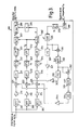
- Fig. 1 shows an example of the general arrangement of a phase modulation type optical fiber gyro according to a first embodiment of the present invention.
- a light beam from a light source 10 propagates via a first fiber coupler 21 and a polarizer 30 and reaches a second fiber coupler 22, in which the beam branches into two light beams that propagate through a fiber loop 40 respectively counterclockwise and clockwise.
- These light beams have their light phases modulated by a phase modulator (PM) 50 in accordance with a modulation signal generated by a phase modulator driver circuit (PMPC) 60. This imposes a primary modulation.
- the two beams reach the fiber coupler 22 and are recombined causing an interference beam to be generated.
- the interference beam 1 passes from the fiber coupler 22 to the first fiber coupler 21 via the polarizer 30.
- the interference signal branches into two beams, one of which returns to the light source 10 and the other of which passes to a photoelectric converter circuit 70 employing a photodiode and is output as an interference signal therefrom.
- the interference signal is transmitted to a signal processing circuit 100 and is processed so as to extract the angular velocity of rotation of the optical fiber gyro.
- ⁇ denotes the phase difference of the beams
- K a coefficient which is proportional to the intensity of the beams and the gain of the photoelectric converter circuit
- v a transmission characteristic of the interferometer
- ⁇ S the Sagnac phase difference which is proportional to the rotational angular velocity of rotation.
- ⁇ denotes the propagation delay time of the light wave which propagates through the fiber loop.
- a sinusoidal wave at a frequency f m is employed as the phase modulation signal.
- ⁇ e denotes the effective phase modulation index
- w m 2 ⁇ f m a modulation angular frequency
- ⁇ m a modulation amplitude
- the interference signal P in Eq. (3) is expanded into a Fourier series employing Bessel functions, and it becomes a line spectrum with lines at frequencies f m , 2f m , 3f m , 4f m ....
- the amplitudes of at least three of the lines of the spectrum need to be determined.
- the first-order, second-order and fourth-order frequency components of the phase modulation are extracted from the interference signal by the signal processing circuit 100 to which the technique of equivalent time processing is applied. The arrangement and operation of the signal processing circuit 100 in this embodiment will be described below.
- the arrangement of the signal processing circuit 100 may be divided into the following four sections: a sampling circuit 111 which samples the photoelectrically-converted interference signal and converts the sampled signal into a digital signal; a timer circuit 112 which generates timing signals for the sampling time, processing time, etc; a digital signal processor 180 which executes digital processing on the results of the sampling, so as to determine the angular velocity of rotation; and a control circuit 170 which controls the sampling circuit and the arithmetic processing circuit.
- the processing circuit 100 is thus relatively simple, and the signals at lower frequencies corresponding to the interference signal can be obtained by sampling the interference signal at a sampling frequency different e.g., lower, than the frequency of the interference signal. This gives the advantage that neither high-speed sampling processing nor a high-speed A/D converter is required.
- the sampling circuit 111 has an input buffer 110 which receives the interference signal and adjusts the signal level thereof, a sample-and-hold circuit 120 which samples the output signal of the input buffer at a predetermined frequency, and an A/D converter 130 by which the signal from the sample-and-hold circuit is converted into a digital signal.
- the timer circuit 112 includes a crystal oscillator (OSC) 140, a frequency divider 150 which is formed e.g. by a high-speed TTL and which divides the frequency of the output signal of the oscillator 140, and a programmable timer 160 which receives a clock signal produced by the frequency division of the frequency divider 150.
- This timer 160 supplies the sampling circuit, the digital signal processor 180 and a microcomputer (CPU) 170 with clock signals respectively corresponding thereto.
- the programmable timer 160 operates with reference to the clock signal which is fed from the frequency divider 150.
- a pulse signal is generated at a predetermined frequency f s ; and is applied to the sample-and hold circuit 120 and the A/D converter 130 as a sampling timing.
- the sample-and-hold circuit 120 and the A/D converter 130 perform the above-described operations of sampling and holding the interference signal and A/D converting the sampling timing at the sampling frequency f s .
- the programmable timer 160 generates a square wave signal at the frequency f m of the primary modulation and supplies that square wave to the phase modulator driver circuit 60.
- the phase modulator driver circuit 60 has a filter circuit, and a transistor buffer circuit which drives the phase modulator 50 as a capacitive load.
- the higher harmonic components of the square wave signal received from the programmable timer 160 are removed by filtering by a filter circuit, and a substantially sinusoidal signal at the frequency f m is set as the primary modulation signal so as to drive the phase modulator 50.
- the microcomputer 170 is connected through a bus line with the programmable timer 160, A/D converter 130 and digital signal processor 180.
- the oscillation operation of the programmable timer 160 is controlled by the microcomputer 170.
- the sampling frequency f s and the phase modulation frequency f m are set by the microcomputer 170.
- the microcomputer 170 monitors the A/D conversion operation of the A/D converter 130, and it senses the end of the A/D conversion after receiving the sampling timing signal from the programmable timer 160.
- the interference signal converted into a digital code by the A/D converter 130 is read out of this A/D converter 130 as interference signal data every sampling step by the microcomputer 170.
- the microcomputer 170 transfers the interference signal data to the digital signal processor 180. Since the production of the interference signal data by the A/D converter 130 is synchronous with the sampling timing, the data transfer is also performed at the same frequency as the sampling frequency f s .
- the digital signal processor 180 On receiving the interference signal data from the microcomputer 170, the digital signal processor 180 extracts the component at the phase modulation frequency f m , the component at the second-order harmonic 2f m and the component at the fourth-order harmonic 4f m , which components are contained in the interference signal.
- the equivalent time signal processing is carried out in accordance with the present invention using the techniques referred to above as "down sampling". More specifically, the aliasing signal components ⁇ f etc. of lower frequencies corresponding to the phase modulation frequency components are extracted by using the relationships of Eqs. (6) - (8) below which are expressed in terms of the sampling frequency f s and the phase modulation frequency f m .
- n is an integer.
- Fig. 2 (a) The above situation is illustrated in Fig. 2 (a).
- the generation of the aliasing frequencies resembles the principle of a stroboscope or a sampling scope. It should be noted that f s may be greater or less than f m , although only the latter case will be discussed in detail below.
- the digital signal processor 180 extracts the value of ⁇ f, 2 ⁇ f and 4 ⁇ f frequency components in place of the frequencies f m , 2f m and 4f m .
- the filter calculations in this embodiment will be described below.
- Fig. 3 is a block diagram of the digital arithmetic processing which is executed in the digital signal processor 180. Individual functional blocks are preferably achieved by suitable software, but dedicated circuits may be used.
- the interference signal data items from the microcomputer 170 are input to band-pass filters 201, 202 and 204 of center frequencies ⁇ f, 2 ⁇ f and 4 ⁇ f previously set by the microcomputer and are extracted as the first-order, second-order and fourth-order component signals, respectively.
- Amplifiers 211, 212 and 214 amplify the respective signals to suitable magnitudes.
- the respective signals contain, not only the principle components of the corresponding frequencies ⁇ f, 2 ⁇ f, and 4 ⁇ f, but also noise and other frequency components which have not been completely suppressed by the band-pass filters 201, 202, and 204.
- Multipliers 221, 222 and 224 detect the rspective signals of the first-order, second-order and fourth-order components at high sensitivities by a lock-in operation. More specifically, the first-order component signal from the amplifier 211, for example, is multiplied by the first-order reference signal of a frequency ⁇ f in the multiplier 221. As a result, the output signal of the multipler 221 has a component of frequency 2 ⁇ f and D.C. components and other noise frequency components. The D.C. component is extracted from these components by a low-pass filter 231.
- the above lock-in operation is similar for the second-order and fourth-order component signals.
- the multiplier 222 and a low-pass filter 232 constitute a lock-in detector for the second-order frequency 2 ⁇ f. Therefore, the second-order reference signal of the frequency 2 ⁇ f is input to the multiplier 222.
- the multiplier 224, and a low-pass filter 234 constitute a lock-in detector for the fourth-order frequency 4 ⁇ f, and the fourth-order reference signal of a frequency 4 ⁇ f is used.
- the low-pass filters 231, 232 and 234 are succeeded by diminution sampling units 241, 242 and 244 as shown in Fig. 3.
- the diminution sampling units 241, 242 and 244 sample input data at a frequency f d .
- the diminution frequency f d should normally be lower than the sampling frequency f s and higher than the frequency response to be achieved by the optical fiber gyro.
- Low-pass filters 251, 252 and 254 subject the output data items of the respective diminution sampling units 241, 242 and 244 to filtering. Accordingly, the first-order D.C. signal S1, second-order D.C. signal S2 and fourth-order D.C. signal S4 which are the outputs of the low-pass filters 251, 252 and 254 are proportional to the amplitudes of the ⁇ f, 2 ⁇ f and 4 ⁇ f frequency components contained in the interference signal data items, respectively.
- the ⁇ f, 2 ⁇ f and 4 ⁇ f frequency components in the interference signal data items are the reflexes of the phase modulation frequency f m and the higher harmonic components 2f m and 4f m thereof which are originally contained in the interference signal, so that the D.C. signals S1, S2 and S4 are proportional to the amplitudes of the f m and 2f m and 4f m frequency components in the interference signal respectively.
- Eq. (11) The constant k in Eq. (11) is determined by only the effective phase modulation index ⁇ e .
- the effective phase modulation index ⁇ e fluctuates in dependence on the voltage amplitude of the drive signal produced by the phase modulator driver circuit 60, and in addition, on the characteristics of the phase modulator 50 itself. Consequently, the constant k of Eq. (11) also fluctuates.
- the second ratio signal y compensates for the fluctuations of the effective phase modulation index ⁇ e .
- the constant k can be determined by Eq. (11).
- the relationship between the second ratio signal y and the constant k need not be calculated on each occasion, but the corresponding values thereof can be found by tabulating them in advance.
- a look-up table 270 stores the relationship between the parameters y and k , and it generates the constant k in response to a y input.
- the reference signal whose frequency is equal to the signal frequency to be detected is required for lock-in detection.
- the reference signals are generated by sampling a square wave signal which is synchronous with the phase modulation signal.
- the square wave signal of frequency f m generated by the programmable timer 160 is supplied to the digital signal processor 180 as shown in Fig. 1, and is applied to a digital input terminal 300 as shown in Fig. 3.
- a sampling circuit 310 checks the input state of the input terminal 300, whereupon it provides a numerical value +1 for an input of high level and numerical value -1 for an input of low level. Checking of the input to the input terminal by the sampling circuit 310 is performed every time there is input of interference signal data. Accordingly, the sampling circuit samples the input signal at a period corresponding to the sampling frequency f s and produces a square wave at values +1 or-1.
- the sampling operation of the sampling circuit 310 causes the reflex frequency ⁇ f based on Eq. (6) to appear at the output of the sampling circuit 310.
- a band-pass filter 321 extracts the reflex frequency component ⁇ f from the output signal of the sampling circuit 310.
- the signal at frequency ⁇ f derived by the band-pass filter 321 has its phase adjusted by a phase shifter 331 and has its amplitude set to an appropriate value by an amplifier 341.
- the resulting signal is used as the first-order reference signal.
- the phase adjustment by the phase shifter 331 is important for enhancing the sensitivity of lock-in detection.
- the first-order reference signal is adjusted so as to be substantially in-phase with the first-order component signal to be detected in the multiplier 221, to make optimum the sensitivity of lock-in detection.
- the plus or minus polarity of the angular velocity data for counterclockwise rotation is determined.
- the reference signal In lock-in detection, the reference signal must have a fixed phase relative to the input signal. If this does not happen, the D.C. signal level and polarity of lock-in detection output change with the phase. In this embodiment, all timing operations are derived from the crystal oscillator 140 and the programmable timer 160, and phase relationships do not change.
- the generation of the second-order and fourth-order reference signals are similar to that of the first-order reference signal described above.
- the output signal of the band-pass filter 321 is multiplied by an integer by a multiplier 351.
- a band-pass filter 322 extracts the components of frequency 2 ⁇ f from the integral-times output of the multiplier 352, and the component of frequency 4 ⁇ f is derived from the product by a band-pass filter 324.
- the operations of phase shifters 332, 334 and amplifiers 342, 344 are the same as for the first-order reference signal.
- the interference signal can be sampled at a frequency lower than that of the interference signal, and the sampled signal may be processed by a A/D converter of low operating speed. Therefore, an A/D converter of high speed and high cost in unnecessary, permitting savings in cost and size. Furthermore, the required number of sampling data items decreases, and the time required for calculations etc. may be shortened, to give the advantage that the accuracy of the processing can be enhanced and the time of processing can be shortened.
- the frequency response characteristic of the optical fiber gyro is set at 30 Hz, and an A/D converter of 12 bits is employed as the A/D converter 130.
- the crystal oscillator 140 employed produces a frequency of 40 MHz, which is divided into clock signals at 2.5 MHz of 1/16 frequency and of 5 MHz of 1/8 frequency by the frequency divider 150, the clock signals being respectively fed to the programmable timer 160 and the microcomputer 170.
- a clock signal at a frequency of 40 MHz is fed to the digital signal processor 180. Since the microcomputer 170 has a data bus of 8 bits, data is transferred at two divided steps each handling one byte.
- n 4 which is the closest value to the phase modulation frequency, in accordance with Eqs. (6) to (8).
- the interference signal data items are passed through the band-pass filters 201, 202 and 204 of the digital signal processor 180 whose center frequencies are pre-set at frequencies ⁇ f, 2 ⁇ f and 4 ⁇ f.
- the digital signal processor 180 is operated by a clock signal of 40 MHz, so that a multiplication and an addition can be processed once in 100 nsec. Since the sampling frequency is 5 kHz (a period of 200 sec.), filter calculations based on at most 2000 multiplications and additions are possible.
- the outputs of the band-pass 201, 202 and 204 contain not only the components of the signal frequencies ⁇ f, 2 ⁇ f and 4 ⁇ f bit also other frequency components and noise.
- the ⁇ f, 2 ⁇ f and 4 ⁇ f of components are therefore detected at high sensitivities by the lock-in operation, using the multipliers 221, 222 and 224 and the reference signals (the output signals of the components 341, 342 and 344) equal to the signal frequency components.
- the cut-off frequencies of the low-pass filters 231, 232 and 234 are set at 200 Hz, and D.C. components proportional to the center frequency components of the corresponding band-pass filters are extracted.
- the digital signal processor 180 used in this example executes a floating point calculation having a mantissa part of 4 bits and an exponent part of 6 bits, and the finite calculation makes it difficult to fabricate the filter whose cutoff frequency is very different from the sampling frequency.
- Each of the diminution sampling units 241, 242 and 244 delivers one output data item for ten input data items so that the sampling rate of the output data is changed from 5 kHz to 500 Hz.
- the frequency response of the optical fiber gyro is set at 30 Hz. Therefore frequency components of and above 30 Hz which are contained in the D.C. signals which are the outputs of the diminution sampling units are eliminated by the low-pass filters 251, 252 and 254.
- the outputs of the low-pass filters 251, 252 and 254 are processed by the dividers 261 and 262.
- the processed results are input to the angular velocity calculator 280 and are changed into a rotational angular velocity measurement.
- An optical phase modulator having a structure in which an optical fiber is wound around a piezo-ceramic cylinder may be used in the present invention.
- a phase modulator of this type has a mechanical resonance frequency f r which is determined by the dimenions and material of the piezo-ceramic cylinder.
- the phase modulation frequency f m is usually set in the vicinity of the mechanical resonance frequency f r .
- the voltage amplitude of the phase modulation signal can be reduced by utilizing mechanical resonance.
- the voltage amplitude of the phase modulation signal may be adjusted. Since, however, the mechanical resonance is used in the phase modulator, the phase modulation amplitude depends greatly upon the modulation frequency f m . For this reason, the frequency with which the voltage amplitude of the phase modulation signal reaches an appropriate level and which can mitigate modulation distortion and fluctuation in a modulation characteristic needs to be selected as the phase modulation frequency f m .
- the piezo-ceramic cylinders for use in the phase modulators are baked with the same dimensions and under the same conditions, there is normally a wide variation in the mechanical resonance characteristics.
- the phase modulation frequency f m differs from one phase modulator to another.
- the microcomputer 170 is provided with means 190 for receiving external data, thereby making it possible to set the phase modulation frequency f m at an optimum value in accordance with the mechanical resonance characteristic of each individual phase modulator 50.
- the microcomputer 170 receives the phase modulation frequency f m in the form of data from means 190 and controls the programmable timer 160 so as to generate a square wave signal of this frequency.
- the microcomputer 170 receives the sampling frequency f s in the form of data from the means 190 and controls the programmable time 160 so as to generate the pulses at the sampling timings of this frequency.
- the setting of the data items of the phase modulation frequency f m and sampling frequency f s , with which the reflex frequencies ⁇ f, 2 ⁇ f and 4 ⁇ f determined by Eqs. (6) to (8) have predetermined values, is achieved using the means 190 to control the microcomputer 170. Accordingly, the filter processing steps of the digital signal processor 180 in Fig. 3 for the frequencies ⁇ f, 2 ⁇ f and 4 ⁇ f become arithmetic processing steps which use the same filter coefficients at all times without regard to the value of the phase modulation frequency f m .
- the means 190 described above may provide the microcomputer 170 with either the phase modulation frequency f m or the sampling frequency f s .
- the other frequency may be calculated from the one provided, by the microcomputer 170 in accordance with Eq. (6) under the condition that the reflex frequency ⁇ f is held constant.
- the reflex frequencies ⁇ f, 2 ⁇ f and 4 ⁇ f can be altered so as to satisfy Eqs. (6) to (8) so that the phase modulation frequency f m is provided as external data and that the sampling frequency is held at a constant value.
- the filter calculations of the digital signal processor 180 need to change calculation coefficients in accordance with the alterations of the frequencies ⁇ f, 2 ⁇ f and 4 ⁇ f, and the microcomputer 170 instructs the digital signal processor 180 to change the calculation coefficients.
- the influence of the different characteristics of the phase modulators can be corrected by the means 190 for receiving external data so that the phase modulator 50 need not be of high precision and can have its cost minimized.
- Fig. 4 shows a second embodiment of the present invention.
- the second embodiment differs from the first embodiment only in the method of supplying the external frequency data. Apart from this, other parts of this embodiment are similar to those of the embodiment of Fig. 1 and the same reference numerals are used.
- the second embodiment is furnished with a rewritable nonvolatile memory device 191. Data items representing the phase modulation frequency f m and sampling frequency f s which are set as appropriate for every phase modulator are recorded in the memory device 191.
- the microcomputer 170 reads out the frequency data items from the nonvolatile memory device 191 at the resetting of power-ON, and controls the operation of the programmable timer on the basis of the data items calculation. Similarly, either the reflex frequency or the sampling frequency may be fixed.
- the data items which are set as appropriate for each individual phase modulator are recorded in the nonvolatile memory device 191.
- Fig. 5 shows a third embodiment of the present invention.
- the sampling means, timing generation means, arithmetic means and control means are shown as individual functional elements.
- the third embodiment uses a signal processing LSI 101 in which these elements are integrated on a single substrate.
- the signal processing LSI 101 includes therein a sample-and-hold circuit and an A/D converter as the sampling means, a digital numerical operation circuit as the arithmetic means, and a logical operation circuit and a memory circuit as the control means.
- Part of the memory circuit is a rewritable nonvolatile memory, in which data appropriate for each phase modulator is recorded.
- the control of the timing generation means and the transfer of the interference signal data by the control means, the generation of the phase modulation signal and sampling timings by the timing generation means, and the digital calculation processing of the interference signal by the arithmetic means are the same as in the first embodiment.
- the detector By constructing the detection circuit in the form of a single LSI as described above, the detector can be reduced in size, and the range of applications of the optical fiber gyro may be expanded.
- Fig. 6 shows a fourth embodiment of the present invention.
- the operations of the programmable timer 160 and digital signal processor 180 are somewhat difference from those in the first embodiment, and a signal adder circuit 61 is included as will be described.
- the other components are the same as in the first embodiment, and the same reference numerals are used.
- the programmable timer 160 genetates a first square wave signal of a frequency f m1 and a second square wave signal of a frequency f m2 . These signals are input to the signal adder circuit 61, and the sum thereof is supplied to the phase modulator driver circuit 60. Accordingly, the phase modulator 50 is driven by a phase modulation signal which has both the frequencies f m1 and f m2 as its frequency components. First and second square wave signals are fed to the digital signal processor 1780, and they are utilized for lock-in detection of the frequency components in the same manner as in the first embodiment.
- the beat frequency and the higher harmonic components thereof are used for detection and correction of the Sagnac phase difference.
- reflex frequencies produced by "down sampling” are used.
- the Sagnac phase difference using the beat frequency components of lower frequencies as described above so that the requirements of frequency characteristics at the input ends of the input buffer 110 and sample-and-hold circuit 120 can be mitigated.
- high frequencies may also be used. Since the first embodiment uses the reflex of the fourth-order higher harmonic component of the phase modulation frequency, response of the circuitry is required up to the frequency of the fourth-order higher harmonic component at stages previous to the completion of the sampling. In contrast, in this embodiment, the frequencies of the beat frequency components suffice, and the frequency characteristics of the input buffer 110 and sample-and-hold circuit 120 can be relieved.
- lock-in detection is used to extract the frequency spectrum components by the digital signal processor 180.
- the arrangements and operations of the lock-in detectors are the same as in the first embodiment, and only the frequencies of the reference signals are different.
- the beat frequency B, reflex frequency ⁇ f and sum frequency ⁇ f + B, and the higher harmonics thereof are needed.
- the first and second square wave signals of frequencies f m1 and f m2 are respectively supplied to digital input terminals 400 and 401 of the digital signal processor 180.
- sampling circuits 410 and 411 refer to these signal inputs with the sampling frequency f s and generate numerical sequences of +1 and -1 in accordance with the input logic levels.
- the numerical sequences are respectively input to band-pass filters 420 and 421 having ⁇ f and ⁇ f + B as their center frequencies whereby signals of frequencies ⁇ f and ⁇ f + B ate produced.
- these signals are multiplied by each other using a multiplier 430, and a signal corresponding to the difference frequency B between the signals is derived using a band-pass filter having B as its center frequency.
- these signals of the respective frequencies are multiplied by integers so as to generate higher harmonic components, and they are converted into reference signals of appropriate amplitude levels and phase by phase shifters and amplifiers.
- the beat frequency B becomes 0.75 kHz in accordance with Eq. (14).
- the frequency spectrum of the interference signal is shown in Fig. 7.
- the sampling frequency f s to be 5 kHz
- the reflex frequency component ⁇ f of the first modulation frequency f m1 becomes 0.5 kHz
- the reflex frequency component ⁇ f + B of the beat frequency component (the second modulation frequency component f m2 ) becomes 1.25 kHz.
- the frequency characteristics to be attained may be of the lower frequency owing to the adoption of the present invention. Therefore the apparatus can be simplified, and the number of data items to be handled in the digital processing.
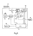
- Fig. 9 shows a fifth embodiment of the present invention.
- the signal procesing circuit 100 of the fifth embodiment is substantially the same as that of the first embodiment, but the former differs from the latter in that it has a rewritable memory device 192 instead of the digital signal processor 180.
- the interference signal is sampled and converted into the digital signal by the sample-and-hold circuit 120 and the A/D converter 130 in accordance with the sampling timings which the programmable timer 160 generates.
- the sampling timing signal from the progammable timer 160 is input to the microcomputer 170, and the sampled values of the interference signal are successively accumulated and stored in the rewritable memory device 192.
- the operation of the microcomputer 170 is divided into a data sampling period and a calculation processing period, which repeat alternately.
- the microcomputer 170 first accumulate a predetermined number of sampled values of the interference signal in the rewritable memory device 192 and subsequently reads out these differences of the interferometer. Then it calculates the angular velocity of rotation detected by the optical fiber gyro.
- the microcomputer 170 reads out the interference signal data sampled in an equivalent time, from the rewritable memory device 192 and thereafter generates a signal waveform for one or more cycles of the time waveform of the interference signal, in the course of calculating the phase differences of the interferometer.
- the frequencies of the interference signal are analysed, on the basis of the composed waveform and using a well-known high-speed Fourier transform method.
- the data sampling and the calculation processing are separated in time, so that the signal processing of the interference sensor is possible without requiring a numerical calculation processing capability of very high speed.
- the phase difference of the interferometer is determined by analyzing the frequency spectrum of the interference signal. As stated below, however, the phase difference of the interferometer can be determined even by computing the waveform moment of the time waveform of the interference signal.
- a0 denotes the D.C. component of the interference signal.
- P′ the waveform moment m of order m is computed as follows:
- ⁇ s denotes the phase difference of the interferometer
- ⁇ 2n and ⁇ 2n denote coefficients which are determined by the effective phase modulation index ⁇ e .
- the m-th-order waveform moment of the interference signal is proportional to cos ⁇ s when m is an even number, and it is proportional to sin ⁇ s when m is an odd number. This is in a dual relationship with the fact that the even-numbered-order frequency spectrum of the interference signal is proportional to cos ⁇ s , while the odd-numbered-ordet frequency spectrum thereof is proportional to sin ⁇ s .
- the phase difference ⁇ s of the interferometer can be determined by computing the waveform moment of the interference signal time waveform instead of calculating the frequency spectrum.
- the calculation of the frequency spectrum and that of the waveform moment may be combined so as to reduce the amount of calculation needed.
- the adoption of the present invention enables the interference sensor to be of high precision and small size, so that the sensor may be applied in various uses.
- Fig. 12 shows an example of a control system when the present invention is applied to sensors for an automobile.
- An interference sensor 511 for measuring the yawing of the car body, an interference sensor 512 for measuring the rolling of the car body, and an interference sensor 510 for measuring the pitching of the car body are respectively installed in an automobile 500. Although, as illustrated, individual sensors are located in different places, they may be collectively located in one place.
- the outputs of the respective sensors are fed to a signal processor 600 and are convered into controlling signals, which are sent to an input/output controller 700.
- This input/output controller 700 is supplied with the detection results of the interference sensors for e.g. a car speed, temperature in the interior of the car etc.
- the output of the yawing sensor which indicates the rotational direction and rotational angle of the automobile, is supplied from the input/output controller 700 to a navigation system.
- the current position of the car is found using the above signal and the distance of travel evaluated by a separate speedometer or the like and is displayed by display means or the like and further the route leading to the destination, etc. may also be displayed.
- the input/output controller 700 sends signals to an engine controller 800, an antiskid brake controller 900, an active suspension controller 550, a car height controller 560 and so forth.
- the antiskid brake controller 900 controls the braking forces of the right and left wheels so as to generate torques opposite in sign to the angular velocity or rotation of the car body based on the signal representing the angular vlocity of rotation from the yawing sensor, and to decrease the absolute value of the signal representing the angular velocity of rotation, thereby to stop the automobile.
- the active suspension controller 550 holds the car body stable while controlling the right and left and front and rear suspension elements so as to generate torques opposite in sign to the angular velocity of rotation from the pitching sensor 510 or the rolling sensor 512, and suppressing the absolute value of the signal representing the angular velocty of rotation so as to decrease that rotation.
- the car receives a signal representing angular velocity from the rolling sensor 512 and holds the car body stable while controlling the suspension elements on the right and left of the car body so as to limit changes in the height of the car body.
- the apparatus of the present invention in an arrangement in which the fiber loop 40 is mounted in a vertical plane so as to detect the rotation of the earth on its own axis, or in which the fiber loop 40 is turned round a vertical axis so as to find an absolute azimuth from a detected change in the angular velocity of the rotation of the earth on its own axis.
- FIG. 13 illustrates such operation.
- components corresponding to components of the interference sensor shown in Fig. 1 are indicated by the same reference numerals.
- the output of the converter (Phase Detector) 70 is amplified by an amplifier 200, and the resulting signal is modulated by a modulator 201.
- the signal from the modulator 201 has effectively had two modulations imposed on it, being the optical modulation imposed on the interfering beam by the optical phase modulator 50, and the second modulation imposed by the modulator 201.
- the modulation frequencies of these two modulations are different.
- the output of the modulator is passed via lock-in amplifiers 202 to an analog to digital and a digital to analog converter 203, which is controlled by the microcomputer 170. That microcomputer 170 also controls the lock-in amplifiers 202 and the phase modulator driver circuit 60.
- the resultant processing is generally similar to the first to fifth embodiments, although sampling is then not necessary. However, it is possible to operate the interference sensor shown in Fig. 13 in combination with the sampling operations described earlier.
- the seventh embodiment of the present invention is shown in Fig. 14. With the exception of the arrangement for modulating the signals, the arrangement is similar to the sixth embodiment of Fig. 13, and the same reference numerals are used for corresponding parts.
- the modulator 201 is omitted, and instead the microcomputer 170 supplies drive signals to the phase modulator drive circuit at two different frequencies f m1 f m2 . These frequencies are different, so that the modulator 50 applies two different optical modulations to the interfering beams in the fiber loop 40.
- the converter 70 detects the interference of those doubly-modulated beams, the signal is amplified via amplifier 200, the resulting input to the lock-in amplifiers 202 is exactly the same as the embodiment of Fig. 13. Therefore, a similar processing may be used, and indeed this can be combined with the sampling arrangement described with reference to the first to fifth embodiments.
- Fig. 15 shows a general view of the interference sensor operating in the time domain, and it can immediately be seen that the general structure is similar to that of the first embodiment of Fig. 1, except that there is a difference in the processing circuit, which is therefore indicated at 1000.
- Other components, which correspond to the interfering sensor of Fig. 1, are indicated by the same reference numerals.
- the eighth embodiment takes the maximum and minimum point of the interference signal waveform as waveform charactetistic points.
- the first embodiment uses the following equations (23) to (25) as design conditions of the optical fiber gyro.
- Effective phase modulation index ⁇ /2 ⁇ ⁇ ⁇ ⁇ Phase difference to be measured :
- Optical phase difference
- the interference signal waveform will be as shown in Fig. 14, with four maximum and minimum points appearing in one cycle of the phase modulation signal.
- the minimum points ⁇ 1, ⁇ 3 are fixed points independent of ⁇ s.
- ⁇ is a constant determined by the phase modulator characteristic and the phase modulator drive signal.
- phase difference to be measured ⁇ s can be determined from equation (26).
- Measuring the phase difference between the maximum and minimum points is equivalent to measuring the time intervals between each point, as is seen from equation (4). So, this embodiment measures the time difference.
- a highly accurate and stable clock can be obtained relatively easily with a quartz oscillator.
- the use of high-speed clock will increase the resolution and therefore the magnitude of the effective digits of measurement, expanding the dynamic range.
- Equation (5) indicates that the change in time position is proportional to the phase change.
- this invention is intended to improve the ease and performance of interference measurement by making use of high precision clocking.
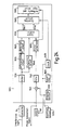
- Fig. 17 shows a block diagram of the signal processing circuit 1000 of the eighth embodiment.
- a photoelectric conversion circuit 70 to convert the interference light into an electric signal and output an interference signal.
- the interference signal from the photoelectric conversion circuit 70 is applied to a differentiating circuit 1010 where it is differentiated.
- a zero-crossing detection circuit 1020 detects the zero-crossing point of the differential signal and generates an extremum timing pulse train representing the times at which the interference signal becomes the maximum or minimum.
- a level comparing circuit 1040 compares the level of the interference signal with a specified threshold level and outputs a rectangular level signal in dependence on the result of comparison.
- a fixed phase pulse generating circuit 1030 generates a specified phase timing by taking as a reference input a modulating signal from the phase modulator drive circuit (PMDC) 60.
- PMDC phase modulator drive circuit
- a count control circuit 105 generates a count start pulse and a count stop pulse for controlling the operation of a counting circuit 106 in dependence on the extremum timing pulse from the zero-crossing detection circuit 102, the fixed timing pulse from the fixed phase pulse generating circuit 103, and the level signal from the comparison circuit 104.
- the counting circuit 106 In response to the count start and stop pulses, the counting circuit 106 counts the clock pulses output from the clock circuit 107.
- An arithmetic and logic unit 108 reads the count value from the counting circuit 106, calculates the phase difference ⁇ s to be measured by using equation (26), and converts that phase difference into a measurement of the angular velocity of rotation.
- a suitable device for detecting the time at which the maximum and minimum of the interference signal occur may be, for example, a peak detection circuit.
- the time waveform of the interference signal may use other characteristic points such as a waveform center, that is determined from the n-th order moment of the time waveform.
- the zero-crossing detection circuit 1020 of this embodiment generates four extremum timing pulses in one cycle of the phase modulation signal.
- this eighth embodiment provides a fixed phase pulse generating circuit 1030, which generates a specified phase timing according to the modulation signal supplied as a reference input from the phase modulator drive circuit 60, and a level comparison circuit 1040 that compares the interference signal level with the specified threshold level and outputs a rectangular level signal according to the result of comparison.
- the count control circuit 1050 generates pulses to start and stop counting, to control the operation of the counting circuit 1060, in dependence on the extremum timing pulse from the zero-crossing detection circuit 1020, the fixed timing pulse from the fixed phase pulse generating cuircuit 1030, and the level signal from the level comparison circuit 1040.
- the count start pulse and the count stop pulse are issued at the maximum point ⁇ 2 and the maximum point ⁇ 4, respectively. Therefore the time interval between the points ⁇ 2 and ⁇ 4 can be measured.
- the counting circuit 1060 counts the clock pulses supplied from the clock circuit 107 according to the count start and stop pulses from the count control circuit 1050.
- the arithmetic and logic unit 1080 reads the count value from the counting circuit 1060 to calculate the phase difference ⁇ s to be measured by using equation (26) and then transforms the calculated phase difference into a rotating angular velocity.
- the fixed timing pulse gives the start timing for this series of operations.
- the phase modulator drive circuit 60 generates a phase modulation signal according to the clock pulses from the count clock generating circuit 1070. Hence, the phase modulator drive circuit 60 and the signal processing circuit 1000 operate in synchronism with each other.
- the modulation characteristic may exhibit a significant temperature dependency. This in turn causes the effective phase modulation index to drift with temperature, causing the output of the gyro to display a characteristic.
- the design conditions for the optical fiber gyro are given by the following equations (27) to (29).
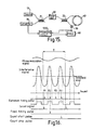
- the time waveform of the interference signal has eight maximum and minimum points during one cycle of the phase modulation signal starting from the zero point of the differential signal, as shown in Figure 18.
- ⁇ 2 and ⁇ 4, and ⁇ 5 to ⁇ 8 are all dependent on the phase difference ⁇ s. Therefore, ⁇ s can be determined by measuring the phase difference or angular velocty of rotation so as to decrease that rotation.
- the car receives a signal representing angular velocity from the rolling sensor 512 and holds the car body stable while controlling the suspension elements on the right and left of the car body so as to limit changes in the height of the car body.
- the apparatus of the present invention in an arrangement in which the fiber loop 40 is mounted in a vertical plane so as to detect the rotation of the earth on its own axis, or in which the fiber loop 40 is turned round a vertical axis so as to find an absolute azimuth from a detected change in the angular velocity of the rotation of the earth on its own axis.
- the count control circuit 1050 generates a count start pulse at the phase timing ⁇ 1 and a first and second count stop pulse at the phase timing ⁇ 2 and ⁇ 3 respectively.
- the arithmetic and logic circuit 1080 solves the equations (30) and (31) as simultaneous equations for ⁇ s and ⁇ .
- the arithmetic and logic circuit 1080 adjusts the control signal to the phase modulator drive circuit 60 to keep at a specified value.
- the process of deriving the rotational angular velocity from the phase difference ⁇ s is the same as that carried out in the eighth embodiment.
- the fixed timing pulse gives the start timing for the above sequence of operations.
- the arithmetic and logic circuit 1080 may compensate for the quantity corresponding to the deviation in the value ⁇ .
- Fig. 20 shows the configuration of the signal processing apparatus 100 of the third embodiment.
- optical fiber gyro of this embodiment is designed are similar to those of the eighth embodiment, except that a local oscillator 160 is provided to introduce a frequency converting means to improve the accuracy of measuring the extremum timing phase difference.
- Fig. 20 shows the configuration of a signal processing apparatus according to the tenth embodiment.
- the local oscillator 1600 generates a locally oscillated signal, which is a sinusoidal wave of angular frequency w z , which is defined as follows.
- w z w m - ⁇ w
- the local oscillation frequency w z differs from the phase modulation angular frequency w m by an angular frequency ⁇ w.
- This oscillator operates according to the clock signals generated by the count clock generating circuit 1070.
- the photoelectric conversion circuit 70 transforms the interference light into an electric signal and thereby generates an interference signal.
- the interference signal outputted from the photoelectric conversion circuit 70 enters the differentiating circuit 1010, where it is differentiated.
- the zero-crossing point of the differential signal is detected by the zero-crossing detection circuit 1020.
- a phase measuring oscillator 110 receives the extremum timing level from the zero-crossing detection circuit 102 and the level signal from the level comparison circuit 104 and generates a measurement-object signal, which is a sinusoidal wave whose zero-crossing point is at the phase of the maximum point. It also receives the fixed timing pulse from the fixed phase pulse generating circuit 103 and generates a measurement reference signal, being a sinusoidal wave whose zero-crossing point is the phase.
- the timing chart of these signals is shown in Fig. 21.
- the angular frequencies of the measuring signal and measurement reference signal are equal to the phase modulation angular frequency w m .
- the measuring signal outputted from the phase measuring oscillator 1100 is supplied to a mixer circuit 1110 where it is multiplied by the locally oscillated signal. Then, the output of the mixer circuit 1110 is fed to a low-pass filter 1130 which extracts only a measurement-object beat signal whose angular frequency is equal to the difference frequency ⁇ w between the phase modulation angular frequency w m and the locally oscillated frequency w z .
- the frequency is changed by extracting, from a signal containing frequency components representing both the sum and difference of angular frequencies of two signals obtained as a result of multiplication, only the frequency component that represents the angular frequency difference.
- the same operation is performed, i.e., the measurement reference signal is fed to a mixer circuit 1120 and a low-pass filter 1140 and converted into a measurement reference beat signal whose angular frequency is equal to ⁇ w.
- the count control circuit 1050 detects the zero-crossing points of the measurement reference beat signal and the measurement beat signal, and generates the count start and stop pulses at the corresponding zero-crossing timing.
- the counting circuit 1060 in response to the instruction of the count start and stop pulses, counts the count clock pulses from the count clock generating circuit 1070.
- the arithmetic and logic circuit 1080 reads the count value from the counting circuit 1060 to calculate the target phase difference ⁇ s and then converts it into a measurement of the angular velocity of rotation.
- the phase modulator drive circuit 60 generates a phase modulation signal according to the count clocks from the count clock generating circuit 1070.
- phase of the measurement reference signal is fixed and known, calculating the angular velocity output of the optical fiber gyro by using the equation (26) needs only measuring the phase difference ⁇ of the measurement signal with respect to the measurement reference signal, as mentioned in the eighth embodiment. Since there are two maximum points in one cycle of the phase modulation signal, as in the eighth embodiment, an alternative is to generate first and second measurement-object signals at these maximum point timings. In this case, the first and second maximums can easily be distinguished from each other by taking the fixed timing pulse as a reference. The phase difference of the light beams can be obtained from the phase difference between the first and second measurement-object signals.
- the measuring signal and the measuring reference signal are mixed with the locally oscillated signal to produce a low-frequency beat signal.
- the measuring signal outputted from the phase measuring oscillator 1100 is fed to the mixer circuit 1110 to be multiplied by the locally oscillated signal.
- the output of the mixer circuit 1110 is passed through the low-pass filter 1130 to be converted into a measurement-object beat signal whose angular frequency is equal to the difference frequency ⁇ w between the phase modulation angular frequency w m and the locally oscillated frequency w z .
- the same operation is carried out also on the measurement reference signal.
- the measurement reference signal is sent to the mixer circuit 1120 and the low-pass filter 1140, and is transformed into a measurement reference beat signal of an angular frequency of ⁇ w.
- T′ 2 ⁇ / ⁇ w
- the low-pass filters 113, 114 have the same phase characteristics, the phase difference between the measurement object signal and the measurement reference signal is retained as the phase difference between the measurement beat signal and the measurement reference beat signal.
- the phase relationship between the measurement-object beat signal and the measurement reference beat signal is identical to that between the measurement-object signal and the measuring reference signal before frequency conversion. Because the frequency has shifted to the beat signal frequency ⁇ w in the low frequency region, the measuring of the phase difference becomes relatively easy.
- the offset phase difference that depends on the phase characteristic of the filter circuits may be examined beforehand and compensated for accordingly.
- the detection of the phase difference between the measurement-object beat signal and the measurement reference beat signal can be realized as in the first embodiment.
- the count control circuit 1050 detects the zero-crossing points of the measurement reference beat signal and the measurement-object beat signal and generates count start and stop pulses at these zero-crossing timings.
- the counting circuit 106 In response to the pulses from the count control circuit 1050, the counting circuit 106 counts the clock pulses, the count value of which is supplied to the arithmetic and logic circuit 1080 which calculates the angular velocity according to equation (26), as the first embodiment.
- the timing relationships between these signals is shown in Fig. 22.
- the tenth embodiment shifts the phase difference measurement to the low frequency range by the frequency conversion, permitting measurement of phase difference or time integral with a higher resolution compared with that of the eighth embodiment when the same clock frequency is used.
- the locally oscillated signal, the measurement-object signal, and the measurement reference signal employ sinusoidal waves.
- the reference signals may be rectangular wave signals or other cyclically recurring signals.
- the mixer circuits 1110, 1120 may be formed by logic circuits using Exclusive-OR gates.
- the frequency conversion employed in the tenth embodiment may be achieved by other means.
- the eleventh embodiment mixed the interference signal and the phase modulation signal with the locally oscillated signal and modulates them into low-frequency signals.
- Fig. 23 shows the configuration of the signal processing circuit 1000 of the eleventh embodiment.
- the mixer circuit 1110 and the low-pass filter 1130 perform frequency conversion of the interference signal, while the mixer circuit 1120 and the low-pass filter 1140 perform frequency conversion of the phase modulator drive signal.
- a waveform shaping circuit 1200 modifies the shape of the locally oscillated signal generated by the local oscillator 1600.
- Other components are identical to those of the eighth embodiment, and corresponding reference numerals are used.
- the design conditions of the optical fiber gyro of this embodiment are the same as those of the eighth embodiment, and the timings of signals are similar, except that the signals are processed in a low frequency range after the frequency conversion.
- the eleventh embodiment includes a shaping circuit 1020 that modifies the shape of the locally oscillated signal generated by the local oscillator 1600.
- the frequency conversion for retaining the time waveform need not be performed. Instead, other frequency conversion may be employed that will retain the correspondence between the signals before and after frequency conversion. In this case, the time intervals between points on the frequency-converted signal that correspond to the waveform characteristic points of the signal before being subjected to the frequency conversion may be measured to determine the phase difference between the interfering signals.
- the twelvth embodiment achieves frequency conversion by modulating the intensity of a light source 70 with a locally oscillated signal. This permits one mixer circuit in the eleventh embodiment to be eliminated. To retain the interference signal waveform in the low frequency region, each of the frequency spectra of the local oscillated signal is made to have equal amplitudes, as in the eleventh embodiment.
- Fig. 24 shows the configuration of the signal processing apparatus of the twelvth embodiment.
- the construction of the signal processing apparatus of the twelfth embodiment is similar to that of the eleventh embodiment except that the mixer circuit for mixing the interference signal and the locally oscillated signal is omitted. Thus, detailed explanation of the configuration of the circuit 1000 is not necessary.
- Embodiments of the invention when applied to an optical fiber gyro have been discussed.
- this invention makes use of general properties of waves and thus can be applied not only to an optical fiber gyro but also to any apparatus or technique whereby physical quantities are measured by the interference of waves, such as phase-modulated electromagnetic waves (including light), sound waves or electron beams.
- the optical phase difference of interfering waves is determined by measuring the phases of the characteristic points of the time waveform, i.e., time position or time interval of the characteristic points. Therefore, because analysis is in the time domain, not the frequency domain, no high-precision operational amplifier or analog digital converter is requited, making the electronic circuit simple.
- This invention also permits compensation of drift of a modulating means such as a phase modulator. Further, unlike systems that measure signal voltage amplitudes by a linear circuit with high accuracy, this invention can expand the dynamic range of interference measurement by using a high-speed clock or a frequency conversion means.
- an interference sensor according to the present invention permits lower frequencies to be processed owing to e.g., the use of "down sampling” and makes it possible to execute digital processing which has not been achievable with known interference sensors handling higher frequencies.
Landscapes
- Physics & Mathematics (AREA)
- Engineering & Computer Science (AREA)
- Radar, Positioning & Navigation (AREA)
- Electromagnetism (AREA)
- Power Engineering (AREA)
- General Physics & Mathematics (AREA)
- Optics & Photonics (AREA)
- Remote Sensing (AREA)
- Gyroscopes (AREA)
- Lasers (AREA)
- Investigating Or Analysing Materials By Optical Means (AREA)
- Instruments For Measurement Of Length By Optical Means (AREA)
- Length Measuring Devices By Optical Means (AREA)
Applications Claiming Priority (2)
| Application Number | Priority Date | Filing Date | Title |
|---|---|---|---|
| JP2049396A JPH03252521A (ja) | 1990-03-02 | 1990-03-02 | 信号処理方法とその回路および干渉センサと物理量検出方法 |
| JP49396/90 | 1990-03-02 |
Publications (3)
| Publication Number | Publication Date |
|---|---|
| EP0444843A2 true EP0444843A2 (fr) | 1991-09-04 |
| EP0444843A3 EP0444843A3 (en) | 1993-01-13 |
| EP0444843B1 EP0444843B1 (fr) | 1996-10-09 |
Family
ID=12829875
Family Applications (1)
| Application Number | Title | Priority Date | Filing Date |
|---|---|---|---|
| EP91301479A Expired - Lifetime EP0444843B1 (fr) | 1990-03-02 | 1991-02-25 | Capteurs interférentiels et méthodes pour mesurer une grandeur physique utilisant tel capteurs aussi bien que système de contrÔle d'un véhicule |
Country Status (4)
| Country | Link |
|---|---|
| EP (1) | EP0444843B1 (fr) |
| JP (1) | JPH03252521A (fr) |
| KR (1) | KR960007745B1 (fr) |
| DE (1) | DE69122524T2 (fr) |
Cited By (4)
| Publication number | Priority date | Publication date | Assignee | Title |
|---|---|---|---|---|
| EP0483993A3 (en) * | 1990-10-29 | 1992-09-23 | Hughes Aircraft Company | Integrated optics gyroscope sensor |
| EP0612976A3 (en) * | 1993-02-23 | 1995-09-20 | Jenoptik Jena Gmbh | Phase modulated interferometer. |
| US20150260143A1 (en) * | 2014-03-11 | 2015-09-17 | Voyomotive, Llc | Method of signaling an engine stop or start request |
| CN109586716A (zh) * | 2018-11-30 | 2019-04-05 | 新奥科技发展有限公司 | 相位分频器和射频电源系统 |
Families Citing this family (5)
| Publication number | Priority date | Publication date | Assignee | Title |
|---|---|---|---|---|
| DE10025395C1 (de) * | 2000-05-23 | 2002-01-17 | Litef Gmbh | Verfahren und Vorrichtung zur optischen Messung einer Differenzgeschwindigkeit und/oder eines Abstandes |
| DE10130159C2 (de) * | 2001-06-22 | 2003-06-18 | Litef Gmbh | Verfahren zur Vermeidung von Bias-Fehlern aufgrund synchroner Einstreuung bei faseroptischen Gyroskopen |
| US7333209B2 (en) * | 2005-11-09 | 2008-02-19 | Honeywell International, Inc. | Fiber optic gyroscope asynchronous demodulation |
| DE112008003233B4 (de) * | 2007-11-27 | 2021-05-06 | Intermodulation Products Ab | Intermodulationsrasterkraftspektroskopie |
| DE102007059536B4 (de) | 2007-12-11 | 2019-06-27 | Robert Bosch Gmbh | Verfahren zum Betrieb einer Sensoranordnung und Sensoranordnung |
Family Cites Families (3)
| Publication number | Priority date | Publication date | Assignee | Title |
|---|---|---|---|---|
| FR2616538B1 (fr) * | 1987-06-11 | 1989-09-01 | Alsthom | Systeme interferometrique a fibre optique de type sagnac |
| JPH01219610A (ja) * | 1988-02-29 | 1989-09-01 | Nissan Motor Co Ltd | 車両用走行方位検出装置 |
| EP0400197B1 (fr) * | 1989-06-02 | 1993-10-06 | LITEF GmbH | Procédé et dispositif pour la démodulation du signal de la vitesse angulaire d'un gyroscope à fibre optique |
-
1990
- 1990-03-02 JP JP2049396A patent/JPH03252521A/ja active Pending
-
1991
- 1991-02-25 DE DE69122524T patent/DE69122524T2/de not_active Expired - Fee Related
- 1991-02-25 EP EP91301479A patent/EP0444843B1/fr not_active Expired - Lifetime
- 1991-03-02 KR KR1019910003439A patent/KR960007745B1/ko not_active Expired - Fee Related
Cited By (5)
| Publication number | Priority date | Publication date | Assignee | Title |
|---|---|---|---|---|
| EP0483993A3 (en) * | 1990-10-29 | 1992-09-23 | Hughes Aircraft Company | Integrated optics gyroscope sensor |
| EP0612976A3 (en) * | 1993-02-23 | 1995-09-20 | Jenoptik Jena Gmbh | Phase modulated interferometer. |
| US20150260143A1 (en) * | 2014-03-11 | 2015-09-17 | Voyomotive, Llc | Method of signaling an engine stop or start request |
| US9951738B2 (en) * | 2014-03-11 | 2018-04-24 | Voyomotive, Llc | Method of signaling an engine stop or start request |
| CN109586716A (zh) * | 2018-11-30 | 2019-04-05 | 新奥科技发展有限公司 | 相位分频器和射频电源系统 |
Also Published As
| Publication number | Publication date |
|---|---|
| KR910017179A (ko) | 1991-11-05 |
| KR960007745B1 (ko) | 1996-06-11 |
| DE69122524D1 (de) | 1996-11-14 |
| EP0444843B1 (fr) | 1996-10-09 |
| DE69122524T2 (de) | 1997-04-24 |
| JPH03252521A (ja) | 1991-11-11 |
| EP0444843A3 (en) | 1993-01-13 |
Similar Documents
| Publication | Publication Date | Title |
|---|---|---|
| EP1627204B1 (fr) | Detecteur de frequence propre pour interferometres a effet sagnac | |
| US5137359A (en) | Digital phase modulator for fiber optic sagnac interferometer | |
| GB2209221A (en) | A demodulator circuit for an interferometer type of hydrophone | |
| EP0444843B1 (fr) | Capteurs interférentiels et méthodes pour mesurer une grandeur physique utilisant tel capteurs aussi bien que système de contrÔle d'un véhicule | |
| JPH03239911A (ja) | 位相変調、強度復調、および回転検知干渉計の制御のための装置 | |
| US5264914A (en) | Interference sensor and method utilizing extracted alliasing frequency components | |
| JP2528199B2 (ja) | 閉ル―プ位相変調装置及び方法 | |
| EP1314002B1 (fr) | Traitement de signaux numeriques pour capteurs a fibres optiques a boucle ouverte | |
| US6028668A (en) | Fiber optic gyroscope having improved readout and modulation index control | |
| JP3051808B2 (ja) | ガス濃度測定装置 | |
| US5684589A (en) | Loop controller for fiber optic gyro with distributed data processing | |
| US5039220A (en) | Optical fiber measuring device, gyrometer, central navigation and stabilizing system | |
| US5262843A (en) | Processing arrangement for optical rate sensor | |
| US4432646A (en) | Angular velocity sensor based on a ring laser | |
| JPH04130212A (ja) | 回転速度の測定のための光ファイバサニャック干渉計 | |
| US5337143A (en) | Loop controller for multiplexed triaxial gyro | |
| JPH07146151A (ja) | ロックイン検出装置 | |
| RU2626019C1 (ru) | Способ повышения точности волоконно-оптического гироскопа с закрытым контуром | |
| JP3077266B2 (ja) | レーザドップラ速度計 | |
| EP0242396B1 (fr) | Detecteur numerique de modulation de frequence synchrone | |
| CN116659644A (zh) | 激光干涉仪 | |
| WO2000003202A1 (fr) | Gyroscope a fibre optique | |
| JP3085725B2 (ja) | 光ファイバジャイロ | |
| EP0649003A1 (fr) | Gyroscopes optiques | |
| KR20070078334A (ko) | 링 레이저 자이로스코프의 각진동 제거 방법 |
Legal Events
| Date | Code | Title | Description |
|---|---|---|---|
| PUAI | Public reference made under article 153(3) epc to a published international application that has entered the european phase |
Free format text: ORIGINAL CODE: 0009012 |
|
| 17P | Request for examination filed |
Effective date: 19910524 |
|
| AK | Designated contracting states |
Kind code of ref document: A2 Designated state(s): DE FR GB |
|
| PUAL | Search report despatched |
Free format text: ORIGINAL CODE: 0009013 |
|
| AK | Designated contracting states |
Kind code of ref document: A3 Designated state(s): DE FR GB |
|
| 17Q | First examination report despatched |
Effective date: 19940808 |
|
| GRAG | Despatch of communication of intention to grant |
Free format text: ORIGINAL CODE: EPIDOS AGRA |
|
| GRAG | Despatch of communication of intention to grant |
Free format text: ORIGINAL CODE: EPIDOS AGRA |
|
| GRAG | Despatch of communication of intention to grant |
Free format text: ORIGINAL CODE: EPIDOS AGRA |
|
| GRAH | Despatch of communication of intention to grant a patent |
Free format text: ORIGINAL CODE: EPIDOS IGRA |
|
| GRAH | Despatch of communication of intention to grant a patent |
Free format text: ORIGINAL CODE: EPIDOS IGRA |
|
| GRAA | (expected) grant |
Free format text: ORIGINAL CODE: 0009210 |
|
| AK | Designated contracting states |
Kind code of ref document: B1 Designated state(s): DE FR GB |
|
| REF | Corresponds to: |
Ref document number: 69122524 Country of ref document: DE Date of ref document: 19961114 |
|
| ET | Fr: translation filed | ||
| PLBE | No opposition filed within time limit |
Free format text: ORIGINAL CODE: 0009261 |
|
| STAA | Information on the status of an ep patent application or granted ep patent |
Free format text: STATUS: NO OPPOSITION FILED WITHIN TIME LIMIT |
|
| 26N | No opposition filed | ||
| PGFP | Annual fee paid to national office [announced via postgrant information from national office to epo] |
Ref country code: DE Payment date: 19991223 Year of fee payment: 10 |
|
| PGFP | Annual fee paid to national office [announced via postgrant information from national office to epo] |
Ref country code: GB Payment date: 20000215 Year of fee payment: 10 |
|
| PG25 | Lapsed in a contracting state [announced via postgrant information from national office to epo] |
Ref country code: GB Free format text: LAPSE BECAUSE OF NON-PAYMENT OF DUE FEES Effective date: 20010225 |
|
| GBPC | Gb: european patent ceased through non-payment of renewal fee |
Effective date: 20010225 |
|
| PG25 | Lapsed in a contracting state [announced via postgrant information from national office to epo] |
Ref country code: DE Free format text: LAPSE BECAUSE OF NON-PAYMENT OF DUE FEES Effective date: 20011201 |
|
| PGFP | Annual fee paid to national office [announced via postgrant information from national office to epo] |
Ref country code: FR Payment date: 20020118 Year of fee payment: 12 |
|
| PG25 | Lapsed in a contracting state [announced via postgrant information from national office to epo] |
Ref country code: FR Free format text: LAPSE BECAUSE OF NON-PAYMENT OF DUE FEES Effective date: 20031031 |
|
| REG | Reference to a national code |
Ref country code: FR Ref legal event code: ST |